Masks of semiconductor devices and methods of forming patterns thereof
US20050175145A1
2005-08-11
11/023,276
2004-12-27
✅ Patent granted
US 7,544,446 B2
2009-06-09
-
-
Mark F Huff | Stewart A Fraser
2026-12-16
Abstract:
Disclosed are a mask of a semiconductor device and a method for forming a pattern thereof, which is capable of correcting a line width bias between a long line width and a short line width when a mask of a semiconductor transistor is formed. The mask may include a plurality of rectangular light shielding patterns formed on a mask disc on which gate line and contact holes are formed; and a connection pattern composed of a plurality of division patterns for selectively connecting the plurality of rectangular light shielding patterns one another. The plurality of rectangular light shielding patterns overlap with the contact hole mask and are formed on both sides of the connection pattern. The connection pattern is divided into 3 to 7 division patterns.
Assignee:
- Dongbu Electronics Co., Ltd. 10 🇰🇷 , South Korea
Interested in similar patents?
Get notified when new applications in this technology area are published.
Classification:
H01L21/0271 » CPC main
Processes or apparatus adapted for the manufacture or treatment of semiconductor or solid state devices or of parts thereof; Manufacture or treatment of semiconductor devices or of parts thereof; Making masks on semiconductor bodies for further photolithographic processing not provided for in group or comprising organic layers
G03F1/36 » CPC further
Originals for photomechanical production of textured or patterned surfaces, e.g., masks, photo-masks, reticles; Mask blanks or pellicles therefor; Containers specially adapted therefor; Preparation thereof Masks having proximity correction features; Preparation thereof, e.g. optical proximity correction [OPC] design processes
G03F1/00 IPC
Originals for photomechanical production of textured or patterned surfaces, e.g., masks, photo-masks, reticles; Mask blanks or pellicles therefor; Containers specially adapted therefor; Preparation thereof
Description
TECHNICAL FIELDThe present disclosure relates to semiconductor devices and, more particularly, to masks of semiconductor devices and a methods of forming patterns thereof.
BACKGROUNDIn general, a mask pattern formation technique employed in fabricating a semiconductor device has a significant affect on accuracy of a pattern formed on the semiconductor device. Particularly, if transmissivity of a mask pattern is not properly considered, a process margin is insufficient, and distortion of a pattern line width, such as shortening of linearity of the line width, occurs contrary to the original purpose of lithographic exposure, which results in deterioration of characteristics of the semiconductor device.
On the other hand, a semiconductor photolithography technique can properly adjust the amount of light passing through a mask by designing the mask elaborately. To this end, an optical proximity correction technique and a phase shifting mask technique have been introduced and various methods for minimizing light distortion due to deformation of a mask pattern have been developed.
Recently, with the development of chemically amplified resists that are very sensitive to light having a far-ultraviolet wavelength of 248 nanometers (nm) or 194 nm, practical techniques for enhancing a resolution have been introduced. Particularly, a technique for forming an auxiliary pattern, which is separated from a main pattern, such as a dummy pattern used to control an optical proximity effect, contributes to enhancement of resolution.
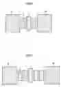
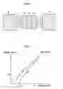
FIGS. 1a and 1b are diagrams showing a long line width and a short line width of an active transistor of a conventional semiconductor mask, respectively.
First, FIG. 1 shows a long line width of about 10 micrometers (μm) of the active transistor of the semiconductor mask. Typically, it is very important to secure the line width of the active transistor overlapping with a gate transistor for normal electrical operation of a gate device. A factor to determine such a characteristic electrically is a characteristic of a high voltage transistor.
The active transistor is composed of portions 2L and 2R in which contact holes 5L and 5R are to be formed and a transistor portion overlapping with a gate transistor. Here, a contour image 4a formed by an exposure apparatus is also shown. In addition, because the active transistor is sufficiently long in its longitudinal direction, a uniform line width is maintained long, as denoted by reference A.
FIG. 1b shows an active transistor related to a low voltage transistor, with a line width designed in the same way as FIG. 1 and with its length decreased. As shown in FIG. 1b, the length of the line width measured on a semiconductor substrate is greatly different from that of the line width in FIG. 1a. Namely, as the line width becomes shortened in its longitudinal direction, the optical proximity effect occurs greatly and the line width is formed somewhat large. Here, a contour image 4b is also shown in FIG. 1b.
In this case, because a transistor portion 3 overlapping with the gate transistor is short in its longitudinal direction, a portion where the line width is uniformly maintained is very short, as denoted by reference B, and electrical characteristics also become unstable. Accordingly, it is difficult to properly fit a characteristic curve for a ratio of breakdown voltage (Vtl) to gate line width or a ratio of saturation current (Idsat) to gate line width.
FIG. 2 is a diagram illustrating optical proximity correction (OPC) applied to enhance a line width of a transistor in the prior art.
As shown in FIG. 2, although the OPC is applied to enhance the line width of the transistor, it is not easy to adjust the linearity of the line width uniformly. This is because patterns to which OPC for line width is applied in programs in common use are corrected by a single way independent of the length of the patterns. Accordingly, correction accuracy is deteriorated when the lengths of line width are different, as described above. Here, reference numeral ML denotes an OPC line width of the active transistor and reference numeral GW denotes a line width of the gate transistor. Particularly, when the line width GW of the gate transistor is wide and the line width ML of the active transistor is narrow, there is a problem in that electrical characteristic are deteriorated.
BRIEF DESCRIPTION OF THE DRAWINGSFIGS. 1a and 1b are diagrams showing a long line width and a short line width of an active transistor of a conventional semiconductor mask, respectively.
FIG. 2 is a diagram illustrating OPC applied in a known manner to enhance a line width of a transistor.
FIG. 3 is a diagram illustrating a first example mask of a semiconductor device.
FIG. 4 is a diagram illustrating a second example mask of a semiconductor device.
FIG. 5 is a diagram illustrating a third example mask of a semiconductor device.
FIG. 6 is a diagram illustrating a fourth example mask of a semiconductor device.
FIG. 7 is a graphical diagram showing line width linearity when a line width of an active transistor is gradually increased, as disclosed herein.
DETAILED DESCRIPTIONA mask of a semiconductor device and a method for forming a pattern thereof, which is capable of correcting a line width bias between a long line width and a short line width when a mask of a semiconductor transistor is formed, is described in detail with reference to the accompanying drawings.
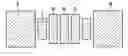
In order to overcome the problem of a conventional small transistor, first, a portion of an active transistor overlapping with a gate line is divided into four division patterns 3a, 3b, and 7. At this time, the division patterns 3a, 3b, and 7 are arranged with a gap of 0.05 μm therebetween, for example. Of these division patterns, a first division pattern 7 has the same line width (vertical length of the division patterns) as in an original design drawing.
At this time, resolution of the division patterns can be defined by a Rayleigh's equation as expressed by Equation 1.
R(Resolution)=k*λ/N.A. Equation 1
Where, k is constant, λ is a wavelength of light emitted from an illuminometer, and N.A. is an aperture of an illuminating lens. For example, when k is 0.5, λ is 0.248, and N.A. is 0.65, resolution (R)=0.19 μm. Accordingly, when a fine pattern having a line width less than the value of the resolution is independently applied to a mask, a pattern for passing light through only the mask physically while an image is not formed in a photosensitive agent can be defined.
Referring to FIG. 3 again, of the division patterns, second patterns 3a and 3b are arranged to be longer by about 0.04 μm than the vertical length of the first pattern 7 in the vertical direction.
In this way, OPC can be applied minimally and the line width can be adjusted very elaborately. In addition, as denoted by reference numeral C, uniformity of the line width can be greatly improved as shown in a contour image 4c.
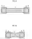
FIG. 4 is a diagram illustrating a second example mask of a semiconductor device. In the arrangement of FIG. 4, three division patterns 3 and 7 are formed and a line width is adjusted by a middle division pattern 3.
FIG. 5 is a diagram illustrating a third example mask of a semiconductor device. In the arrangement of FIG. 5, five division patterns 3 and 7 are formed and a line width is adjusted by a middle division pattern 3.
FIG. 6 is a diagram illustrating a fourth example mask of a semiconductor device, wherein three division patterns 3a, 3b, 3c and 7 are formed and a line width is adjusted by middle division patterns 3a, 3b and 3c.
FIG. 7 is a graphical diagram showing line width linearity when a line width of an active transistor is gradually increased, as disclosed herein. In the graphical diagram, a B curve shows a result of application of the conventional method and a C curve shows a result of selective application of the disclosed division patterns. The disclosed techniques and patterns can minimize the line width bias between the small-scale transistor and the transistor having a large length by selectively dividing the line width of the small-scale transistor in the active region.
As is apparent from the above description, because a line width of a small-scale transistor in an active region is selectively divided, a line width bias between the line width of the small-scale transistor and a transistor having a large length can be minimized. In addition, because the line width of the small-scale transistor can be maintained uniformly, a breakdown voltage and saturation current in a portion overlapping with a gate transistor can be optimized.
In addition, because electrical characteristics of NMOS and PMOS in memory devices can be maintained symmetrically, the yield of devices can be enhanced.
As disclosed herein, a mask of a semiconductor device and a method for forming a pattern thereof, which is capable of forming an accurate line width by correcting a line width bias between a long line width and a short line width when a mask of a semiconductor transistor is formed.
According to one example, a mask of a semiconductor device may include a plurality of rectangular light shielding patterns formed on a mask disc on which gate line and contact holes are formed; and a connection pattern composed of a plurality of division patterns for selectively connecting the plurality of rectangular light shielding patterns one another.
In one example, the plurality of rectangular light shielding patterns overlap with the contact hole mask and are formed on both sides of the connection pattern. Additionally, the connection pattern may be divided into 3 to 7 division patterns.
In one arrangement, at least one of the plurality of division patterns overlaps with the gate line. The division pattern overlapping with the gate line may have a length selectively different from those of division patterns, which do not overlap with the gate line.
According to a second example, there is provided a method for forming a mask pattern for a semiconductor device. Such a method may also include forming a plurality of rectangular light shielding patterns on a mask disc on which gate line and contact holes are formed; and forming a plurality of division patterns for selectively connecting the plurality of rectangular light shielding patterns one another.
In one example, the plurality of rectangular light shielding patterns overlap with the contact hole mask and are formed on both sides of the plurality of division pattern. Additionally, the plurality of division pattern may be divided into 3 to 7 division patterns.
With the configurations as above, because a line width of a small-scale transistor in an active region is selectively divided, a line width bias between the line width of the small-scale transistor and a transistor having a large length can be minimized. In addition, because the line width of the small-scale transistor can be maintained uniformly, a breakdown voltage and saturation current in a portion overlapping with a gate transistor can be optimized.
This patent application makes reference to, incorporates the same herein, and claims all benefits accruing under 35 U.S.C. § 119 from an application for MASK OF SEMICONDUCTOR DEVICE AND METHOD FOR FORMING PATTERN THEREOF filed in the Korean Industrial Property Office on Dec. 27, 2003 and there duly assigned Serial No. 10-2003-0098324.
Although certain apparatus constructed in accordance with the teachings of the invention have been described herein, the scope of coverage of this patent is not limited thereto. On the contrary, this patent covers every apparatus, method and article of manufacture fairly falling within the scope of the appended claims either literally or under the doctrine of equivalents.
Claims
1. A mask used in fabricating a semiconductor device, comprising:
a plurality of rectangular light shielding patterns formed on a mask disc on which gate line and contact holes are formed; and
a connection pattern composed of a plurality of division patterns for selectively connecting the plurality of rectangular light shielding patterns one another.
2. The mask of claim 1, wherein the plurality of rectangular light shielding patterns overlap with the contact hole mask and are formed on both sides of the connection pattern.
3. The mask of claim 1, wherein the connection pattern is divided into 3 to 7 division patterns.
4. The mask of claim 1 or 3, wherein at least one of the plurality of division patterns overlaps with the gate line.
5. The mask of claim 4, wherein the division pattern overlapping with the gate line has a length selectively different from those of division patterns, which do not overlap with the gate line.
6. A method for forming a mask pattern used in fabricating a semiconductor device, comprising:
forming a plurality of rectangular light shielding patterns on a mask disc on which gate line and contact holes are formed; and
forming a plurality of division patterns for selectively connecting the plurality of rectangular light shielding patterns one another.
7. The method of claim 6, wherein the plurality of rectangular light shielding patterns overlap with the contact hole mask and are formed on both sides of the plurality of division pattern.
8. The method of claim 6, wherein the plurality of division pattern are divided into 3 to 7 division patterns.
Images & Drawings included:
Sources:
- United States Patent and Trademark Office - verify current appl. status at the USPTO↗
Similar patent applications:
Recent applications in this class:
- » 20250239451 2025-07-24
HARDMASK COMPOSITION, HARDMASK LAYER, AND METHOD OF FORMING PATTERNS - » 20250226218 2025-07-10
FILM FORMING METHOD, ARTICLE MANUFACTURING METHOD, AND CURABLE COMPOSITION - » 20250174458 2025-05-29
DIRECTED SELF-ASSEMBLY ENABLED PATTERNING OVER METAL LAYERS USING ASSISTING FEATURES - » 20250166993 2025-05-22
METHODS OF FORMING NANOSTRUCTURES UTILIZING SELF-ASSEMBLED NUCLEIC ACIDS - » 20250157817 2025-05-15
FILM FORMING METHOD, ARTICLE MANUFACTURING METHOD AND FILM FORMING APPARATUS - » 20240371638 2024-11-07
PHOTORESIST DEVELOPER AND METHOD OF DEVELOPING PHOTORESIST - » 20240162038 2024-05-16
PHOTOMASK STRUCTURE, SEMICONDUCTOR STRUCTURE AND MANUFACTURING METHOD THEREOF - » 20240153768 2024-05-09
METHOD FOR MANUFACTURING SEMICONDUCTOR SUBSTRATE AND COMPOSITION - » 20230386833 2023-11-30
Selective metal removal with flowable polymer - » 20230377883 2023-11-23
SYSTEM AND METHOD FOR DIRECTED SELF-ASSEMBLY WITH HIGH BOILING POINT SOLVENT
Recent applications for this Assignee:
- » 20080156987 2008-07-03
Method of TEM sample preparation for electron holography for semiconductor devices - » 20070152240 2007-07-05
Bipolar junction transistor and manufacturing method thereof - » 20070111445 2007-05-17
Flash memories and methods of fabricating the same - » 20070032019 2007-02-08
Flash memory device and method for fabricating the same - » 20070012963 2007-01-18
CMOS image sensor and manufacturing method thereof - » 20060146460 2006-07-06
Method of simulating semiconductor integrated circuit - » 20060040464 2006-02-23
Semiconductor device and method for fabricating the same - » 20050282348 2005-12-22
Method of manufacturing thin film capacitor - » 10733884 2005-11-15
Method of manufacturing a semiconductor device