Voltage regulator having overcurrent protection circuit and method manufacturing voltage regulator
US20050185490A1
2005-08-25
11/061,495
2005-02-18
✅ Patent granted
US 7,411,376 B2
2008-08-12
-
-
Gary L Laxton | Ramy Ramadan
2025-08-08
Abstract:
The present invention provides a voltage regulator having an overcurrent protection circuit capable of precisely setting a load current permitting an overcurrent protecting function to be valid. A measurement circuit including at least one element equivalent to an element as a constituent element of an overcurrent protection circuit of a voltage regulator is provided in the voltage regulator. Characteristics of the at least one element are measured thereby trimming the element of the overcurrent protection circuit.
Assignee:
- Seiko Instruments Inc. 772 🇯🇵 , Japan
Interested in similar patents?
Get notified when new applications in this technology area are published.
Classification:
G05F1/575 » CPC main
Automatic systems in which deviations of an electric quantity from one or more predetermined values are detected at the output of the system and fed back to a device within the system to restore the detected quantity to its predetermined value or values, i.e. retroactive systems; Regulating voltage or current wherein the variable actually regulated by the final control device is dc using semiconductor devices in series with the load as final control devices characterised by the feedback circuit
G11C5/147 » CPC further
Details of stores covered by group; Power supply arrangements, e.g. power down, chip selection or deselection, layout of wirings or power grids, or multiple supply levels Voltage reference generators, voltage or current regulators; Internally lowered supply levels; Compensation for voltage drops
G05F1/573 IPC
Automatic systems in which deviations of an electric quantity from one or more predetermined values are detected at the output of the system and fed back to a device within the system to restore the detected quantity to its predetermined value or values, i.e. retroactive systems; Regulating voltage or current wherein the variable actually regulated by the final control device is dc using semiconductor devices in series with the load as final control devices sensing a condition of the system or its load in addition to means responsive to deviations in the output of the system, e.g. current, voltage, power factor for protection with overcurrent detector
H05H7/00 IPC
Details of devices of the types covered by groups
H05H7/00 IPC
Details of devices of the types covered by groups
H02H9/00 IPC
Emergency protective circuit arrangements for limiting excess current or voltage without disconnection
Description
BACKGROUD OF THE INVENTION1. Field of the Invention
The present invention relates in general to a voltage regulator, and more particularly to an overcurrent protection circuit for a voltage regulator.
2. Description of the Related Art
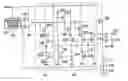
FIG. 3 shows a configuration of a conventional overcurrent protection circuit for a voltage regulator. A reference voltage source 101 supplies a constant-voltage Vref to an inverted input terminal of an error amplifier 102. An output of the error amplifier 102 is connected to a gate of a PMOS output driver transistor 105, and is also connected to a gate of a first PMOS sense transistor 106, a gate of a second PMOS sense transistor 115, and a drain of a PMOS transistor 107 of an overcurrent protection circuit 103. A source of the PMOS output driver transistor 105 is connected to an input terminal IN and a drain of the same is connected to an output terminal OUT. A load resistor 114, a capacitor 113, and a voltage dividing circuit 104 consisting of resistors 111 and 112 are connected to the output terminal OUT. The voltage dividing circuit 104 supplies a divided voltage of an output voltage VOUT to a non-inverted input terminal of the error amplifier 102.
The overcurrent protection circuit 103 includes: the first and second PMOS sense transistors 106 and 115; the PMOS transistor 107; an NMOS transistor 108; resistors 109 and 110; first, second, and third PMOS level shifters 120, 119, and 118; and NMOS transistors 116 and 117 constituting a current mirror circuit. Here, the PMOS output driver transistor 105 has a gate width which is several times (e.g., 100,000 times) as large as that of the first PMOS sense transistor 106 for monitoring a load current Iout of the voltage regulator. Also, the PMOS output driver transistor 105 is designed so as to show a mirror relationship with the first and second PMOS sense transistors 106 and 115.
The conventional overcurrent protection circuit for a voltage regulator shown in FIG. 3 operates as follows.
If an amount of load current Iout supplied by the PMOS output driver transistor 105 to the load 114 is little, a current Isense flowing to the first PMOS sense transistor 106 is small in proportion to it. Thus, a voltage difference generated across the resistor 109 is also small and the NMOS transistor 108 is in a non-conductive state. Therefore, since a current does not flow to the NMOS transistor 108, a voltage difference is not generated across the resistor 110 and the PMOS transistor is also in a non-conductive state.
However, when a load current Iout supplied by the PMOS output driver transistor 105 to the load 114 increases, a current Isense flowing to the first PMOS sense transistor 106 also increases in proportion to it and a voltage generated across the resistor 109 also increases. Thus, the NMOS transistor 108 is in a conductive state. When the NMOS transistor 108 becomes conductive and a voltage difference generated across the resistor 110 increases, the PMOS transistor 107 conducts to increase a gate voltage of the PMOS output driver transistor 105. Thus, a driving ability of the PMOS output driver transistor 105 decreases and an output voltage OUT falls. In this way, elements are prevented from being destroyed by an overload current.
Moreover, operating states of the PMOS output driver transistor 105 and the first PMOS sense transistor 106 are usually made identical to each other based on an operation of a circuit including the second PMOS sense transistor 115, the first, second, and third PMOS level shifters 120, 119, and 118, and the NMOS transistors 116 and 117 constituting the current mirror circuit. In this case, a ratio between a value of a current caused to flow through the PMOS output driver transistor 105 and a value of a current caused to flow through the first PMOS sense transistor 106 is determined based on a transistor size ratio between the PMOS output driver transistor 105 and the first PMOS sense transistor 106. Thus, it is possible to set a load current Ipro permitting the overcurrent protecting function to be valid (refer to JP 2003-29856 A (pp. 1 to 6, and FIG. 1)).
However, the conventional overcurrent protection circuit for a voltage regulator involves a problem in that dispersion occurs in the load current Ipro permitting the overcurret protecting function to be valid due to manufacture dispersion. That is, a threshold voltage value Vth of the NMOS transistor 108 disperses. Moreover, the transistor size ratio between the PMOS output driver transistor 105 and the first PMOS sense transistor 106 also disperses due to the manufacture dispersion. Consequently, as shown in FIG. 4, the load current Ipro permitting the overcurrent protecting function to be valid greatly disperses from a target load current value Itype.
SUMMARY OF THE INVENTIONIn order to solve the problems described above, a measurement circuit including at least one element as a constituent element of a voltage regulator is added to an overcurrent protection circuit for a voltage regulator according to the present invention. More specifically, for example, a resistance value of the resistor 109 is trimmed based on a substantially actually measured value of the current Isense which is caused to flow through the first PMOS sense transistor 106 in proportion to the load current Ipro permitting the overcurrent protecting function to be valid, and a substantially actually measured value of the threshold voltage value Vth of the NMOS transistor 108 using the measurement circuit, whereby the manufacture dispersion of the set load current IPro permitting the overcurrent protecting function to be valid is made small.
In addition, a third PMOS sense transistor having the same transistor size as that of the first PMOS sense transistor, and a fourth PMOS level shifter are added, whereby the operating states of the first and third PMOS sense transistors are made usually identical to each other, and thus a current caused to flow through the first PMOS sense transistor and a current caused to flow through the third PMOS sense transistor become equal to each other. Moreover, the first and third PMOS sense transistors are disposed so as to be adjacent to each other in terms of layout, thereby minimizing differences in transistor size and characteristics between the first and third PMOS sense transistors due to the manufacture dispersion. As a result, the current Isense which is caused to flow through the first PMOS sense transistor in proportion to the load current is obtained based on the measurement for the current caused to flow through the third PMOS sense transistor.
In addition, an NMOS transistor having the same transistor size as that of the NMOS transistor 108 is added, and the NMOS transistor 108 and the added NMOS transistor are disposed so as to be adjacent to each other in terms of the layout, thereby minimizing a difference in threshold voltage value Vth between the NMOS transistor 108 and the added NMOS transistor due to the manufacture dispersion. The threshold voltage value Vth of the added NMOS transistor is actually measured, thereby obtaining the threshold voltage value Vth of the NMOS transistor 108. Thus, the resistance value of the resistor 109 is adjusted through the trimming using those actually measured values, whereby the dispersion of the set load current Ipro permitting the overcurrent protecting function to be valid is made small.
In the overcurrent protection circuit for a voltage regulator according to the present invention, it is possible to substantially measure the current Isense which is caused to flow through the first PMOS sense transistor 106 in proportion to the load current Ipro permitting the overcurrent protecting function to be valid, and the threshold voltage value Vth of the NMOS transistor 108. The resistance value of the resistor 109 is trimmed using those actually measured values, whereby it is possible to make small the manufacture dispersion of the set load current Ipro permitting the overcurrent protecting function to be valid.
BRIEF DESCRIPTION OF THE DRAWINGSIn the accompanying drawings:
FIG. 1 is a circuit diagram showing a configuration of a voltage regulator according to a first embodiment of the present invention;
FIG. 2 is a circuit diagram showing a configuration of a voltage regulator according to a second embodiment of the present invention;
FIG. 3 is a circuit diagram showing a configuration of a conventional voltage regulator;
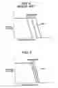
FIG. 4 is a graphical representation showing a relationship between a load current and an output voltage in the conventional voltage regulator; and
FIG. 5 is a graphical representation showing a relationship between a load current and an output voltage in the voltage regulator of the present invention.
DETAILED DESCRIPTION OF THE PREFERRED EMBODIMENTSEmbodiments of the present invention will hereinafter be described in detail with reference to the accompanying drawings.
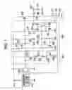
First EmbodimentFIG. 1 is a circuit diagram showing a configuration of a voltage regulator according to a first embodiment of the present invention.
A reference voltage source 101 supplies a constant voltage Vref to an inverted input terminal of an error amplifier 102. An output terminal of the error amplifier 102 is connected to a gate of a PMOS output driver transistor 105, and a gate of a first PMOS sense transistor 106, a gate of a second PMOS sense transistor 115, and a drain of a PMOS transistor 107 in an overcurrent protection circuit 103. A source of the PMOS output driver transistor 105 is connected to an input terminal IN, a drain of the PMOS output driver transistor 105 is connected to an output terminal OUT. A load resistor 114, and a capacitor 113, and a voltage dividing circuit 104 constituted by resistors 111 and 112 are connected to the output terminal OUT. The voltage dividing circuit 104 supplies a voltage obtained through the voltage division of an output voltage VOUT to a non-inverted input terminal of the error amplifier 102.
The overcurrent protection circuit 103 is connected between an output terminal of the error amplifier 102 and the gate terminal of the PMOS output driver transistor 105 in order to monitor the load current Iout supplied from the PMOS output driver transistor 105 to control an overcurrent of the load current Iout.
A measurement circuit 201 includes a third PMOS sense transistor 202 having the same transistor size as that of the first PMOS sense transistor 106 of the overcurrent protection circuit 103, a fourth PMOS level shifter 203 having the same transistor size as that of the first PMOS level shifter 120 of the overcurrent protection circuit 103, an NMOS transistor 204 having the same transistor size as that of the NMOS transistor 108 of the overcurrent protection circuit 103, and a fuse 205.
A source of the third PMOS sense transistor 202 is connected to a source of the first PMOS sense transistor 106, a gate of the third PMOS sense transistor 202 is connected to the gate of the first PMOS sense transistor 106, and a drain of the third PMOS sense transistor 202 is connected to a source of the fourth PMOS level shifter 203. Agate of the fourth PMOS level shifter 203 is connected to each of gates of the first, second, and third PMOS level shifters 120, 119, and 118. Also, a drain of the fourth PMOS level shifter 203 is connected to a measurement terminal TEST through the fuse 205. Both a gate and a drain of the NMOS transistor 204 are reconnected to the measurement terminal TEST.
Since the first and third PMOS sense transistor 106 and 202 have the same transistor size and thus are equal in gate to source voltage to each other, a current caused to flow through the third PMOS sense transistor 202 becomes equal to a current caused to flow through the first PMOS sense transistor 106. A current caused to flow through the fourth PMOS level shifter 203 also becomes equal to a current caused to flow through the first PMOS level shifter 120. Thus, the first and fourth PMOS level shifters 120 and 203 also become equal in gate to source voltage to each other. In other words, a voltage at a node C also becomes nearly equal to a voltage at a node A. Consequently, the first and third PMOS sense transistors 106 and 202 also become equal in source to drain voltage to each other, and hence are usually identical in operating state to each other.
The first and third PMOS sense transistors 106 and 202 are disposed so as to be adjacent to each other in terms of the layout, thereby minimizing differences in transistor size and characteristics between the first and third PMOS sense transistors 106 and 202 due to the manufacture dispersion. Consequently, a current Isense caused to flow through the first PMOS sense transistor 106 and a current caused to flow through the third PMOS sense transistor 202 usually become equal to each other.
In addition, the NMOS transistors 108 and 204 are disposed so as to be adjacent to each other in terms of the layout, thereby minimizing a difference in threshold voltage value Vth between the NMOS transistors 108 and 204 due to the manufacture dispersion.
Next, a procedure for setting a load current Ipro permitting the overcurrent protecting function to be valid will be described with reference to FIG. 1.
First of all, an input voltage is applied to the input terminal IN and a resistance value of the load resistor 114 is then adjusted in order to obtain the load current Ipro permitting the overcurrent protecting function to be valid. An ammeter is inserted between the measurement terminal TEST and the ground to measure a current Im which is being caused to flow through the third PMOS sense transistor 202. The measured current Im is equal to the current Isense which is being caused to flow through the first PMOS sense transistor 106. Hence, the current Im is judged as the current Isense which is being caused to flow through the first PMOS sense transistor 106 so as to permit the overcurrent protecting function to be valid.
Next, in a state in which no input voltage is applied to the input terminal IN, a constant current is injected to the measurement terminal TEST in order to measure a voltage appearing at the measurement terminal TEST. The threshold voltage value Vth of the NMOS transistor 204 can be calculated from the measured voltage value. The NMOS transistors 108 and 204 are nearly equal in threshold voltage value Vth to each other. Hence, the threshold voltage value Vth of the NMOS transistor 204 is judged as the threshold voltage value Vth of the NMOS transistor 108.
Consequently, a target resistance value of the resistor 109 can be calculated from the actually measured current Im caused to flow through the first PMOS sense transistor 106, and the actually measured threshold voltage value Vth of NMOS transistor 108. The trimming of the resistance value of the resistor 109 to the target resistance value makes it possible to precisely set the load current IPro permitting the overcurrent protecting function to be valid.
In addition, in case of no provision of the NMOS transistor 204 in the measurement current 201 of FIG. 1, there is offered an effect that even when there is the dispersion in the transistor size ratio between the PMOS output driver transistor 105 and the first PMOS sense transistor 106 due to the manufacture dispersion, if only the current Isense being caused to flow through the first PMOS sense transistor 106 is measured, the dispersion in the load current Ipro permitting the overcurrent protecting function to be valid can be reduced through the trimming of the resistance value of the resistor 109.
FIG. 5 shows current dispersion characterstics of the first embodiment. The horizontal and the vertical axes indicate load current and output voltage, respectively, and the graph shows load current Ipro. As shown in FIG. 5, the load current Ipro permitting the overcurrent protecting function to be valid of the first embodiment disperses from a target load current value Itype smaller than that of the prior case shown in the FIG. 4.
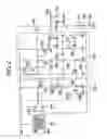
Second EmbodimentFIG. 2 is a circuit diagram showing a configuration of a voltage regulator according to a second embodiment of the present invention. The measurement circuit 201 includes a resistor 206 connected between the fuse 205 and the ground, and an NMOS transistor 204 having a source connected to the ground, a drain connected to the measurement terminal TEST, and a gate connected to a node between the fuse 205 and the resistor 206 instead of the NMOS transistor 204 connected between the fuse 205 and the ground in the circuit shown in FIG. 1. A resistance value of the resistor 206 is proportional to the resistance value of the resistor 109. Also, the resistors 206 and 109 are disposed so as to be adjacent to each other in terms of the layout, thereby minimizing differences in proportional relationship of the element size and characteristics between the resistors 206 and 109 due to the manufacture dispersion. In such a manner, the measurement circuit 201 is made an overcurrent detecting circuit equivalent to the actual circuit. It is obvious that the resistance value of the resistor 206 is set so that the load current Ipro permitting the NMOS transistor 204 of the measurement circuit 201 to become a conductive state becomes a target load current value Itype, and the resistance value of the resistor 109 is trimmed in proportion to the set resistance value of the resistor 206, thereby obtaining the same effect as that in Embodiment 1.
Moreover, the voltage regulator according to this embodiment of the present invention includes power saving means for, after the load current Ipro permitting the overcurrent protecting function to be valid is set, electrically disconnecting the measurement circuit 201 from the voltage regulator through the melting of the fuse 205 or the like, thereby preventing a current unnecessary for the actual operation of the voltage regulator from being consumed.
While the first and second embodiments have been described with reference to FIGS. 1 and 2, respectively, the voltage regulator of the present invention is not intended to be limited to any of the configurations shown in the circuit diagrams of the first and second embodiments of FIGS. 1 and 2. That is, the various characteristics of the voltage regulator are adjusted using the measurement circuit 201 including at least one element equivalent to the element as the constituent element of the overcurrent protection circuit of the voltage regulator, thereby allowing a highly precise voltage regulator to be realized.
DESCRIPTION OF SYMBOLS
- 101 reference voltage source
- 103 overcurrent protection circuit
- 104 voltage dividing circuit
- 201 measurement circuit
Claims
1. A voltage regulator, comprising:
a measurement circuit including at Least one element as a constituent element of the voltage regulator,
wherein the constituent element of the voltage regulator is trimmed based on an actually measured value of the measurement circuit to adjust characteristics of the voltage regulator.
2. A voltage regulator according to claim 1, further comprising:
a sense transistor for monitoring a load current; and
a circuit for measuring characteristics of an element as a constituent element of an overcurrent protection circuit,
wherein the overcurrent protection circuit is trimmed based on an actually measured value of the element characteristics, thereby making it possible to set a load current permitting an overcurrent protecting function to be valid.
3. A voltage regulator according to claim 2, wherein the overcurrent protection circuit is trimmed based on an actually measured value of a current caused to flow through the sense transistor, thereby making it possible to set the load current permitting the overcurrent protecting function to be valid.
4. A voltage regulator according to claim 2, wherein at least the load current of the voltage regulator and a current caused to flow through the sense transistor are measured to obtain actually measured values, and the overcurrent protection circuit is trimmed based on the actually measured values, thereby making it possible to set the load current permitting the overcurrent protecting function to be valid.
5. A voltage regulator according to claim 1, further comprising power saving means for preventing a current unnecessary for an actual operation of the voltage regulator from being consumed after a load current permitting an overcurrent protecting function to be valid is set.
6. A voltage regulator, comprising:
a first constituent element;
a second constituent element; and
a measurement constituent element,
wherein the first constituent element and the measurement constituent element are provided so as to be adjacent to each other, and the second constituent element is trimmed based on an actually measured value of the measurement constituent element.
7. A voltage regulator according to claim 6, further comprising an overcurrent protection circuit including the first constituent element and the second constituent element.
8. A method of manufacturing a voltage regulator comprising a first constituent element, a second constituent element, and a measurement constituent element, comprising the steps of:
measuring characteristics of the measurement constituent element; and
trimming the second constituent element based on results of the measurement of the characteristics of the measurement constituent element.
Images & Drawings included:
Sources:
- United States Patent and Trademark Office - verify current appl. status at the USPTO↗
Recent applications in this class:
- » 20250291376 2025-09-18
Voltage Regulator for Providing a Stable Output Voltage in an Implantable Stimulator Device - » 20250291375 2025-09-18
LOW-NOISE VOLTAGE REGULATORS AND ASSOCIATED METHODS - » 20250291374 2025-09-18
LOW-DROPOUT (LDO) REGULATOR WITH AGGRESSOR CURRENT CANCELLATION - » 20250278105 2025-09-04
Regulator Circuit, Circuit Device, And Oscillator - » 20250278104 2025-09-04
FAST SETTLED AND TRANSIENT LOW DROPOUT (LDO) REGULATOR - » 20250271887 2025-08-28
LDO REGULATOR, METHOD OF OPERATING THE SAME, AND POWER MANAGEMENT DEVICE INCLUDING THE SAME - » 20250271886 2025-08-28
LDO REGULATOR CIRCUIT APPARATUS CAPABLE OF ATTENUATING SUPPLY VOLTAGE NOISE - » 20250271885 2025-08-28
LOW-PROFILE POWER SUPPLY REGULATOR UTILIZING FLIPPED VOLTAGE FOLLOWER - » 20250244784 2025-07-31
LOW-DROPOUT (LDO) VOLTAGE REGULATOR - » 20250244783 2025-07-31
Source Follower Type Regulator with DAC feedback
Recent applications for this Assignee:
- » 20190264742 2019-08-29
Method of manufacturing an enveloping layer-coated slide bearing - » 20190025766 2019-01-24
Timepiece, timepiece system, and method of controlling timepiece - » 20180306243 2018-10-25
Rolling bearing - » 20180306242 2018-10-25
Structure with thermoplastic elastomer enveloping layer, bearing, and drive module - » 20180306240 2018-10-25
Enveloping layer-coated slide bearing and drive module - » 20180241280 2018-08-23
Vibration generation device and electronic device - » 20180203417 2018-07-19
Timepiece - » 20180097302 2018-04-05
Portable printer - » 20170331349 2017-11-16
Vibration generation device and electronic apparatus - » 20170315509 2017-11-02
Mechanical component, mechanical component manufacturing method, movement, and timepiece