Command multiplier for built-in-self-test
US20050193253A1
2005-09-01
10/708,184
2004-02-13
✅ Patent granted
US 7,194,670 B2
2007-03-20
-
-
Cynthia Britt
2025-04-07
Abstract:
Disclosed is a flexible command multiplication scheme for the built-in-self test (BIST) of a high-speed embedded memory array that segments BIST functionality into remote lower-speed executable instructions and local higher-speed executable instructions. A stand-alone BIST logic controller operates at a lower frequency and communicates with a command multiplier using a low-speed BIST instruction seed set. The command multiplier uses offset or directive registers to drive a logic unit or ALU to generate “n” sets of CAD information which are then time-multiplexed to the embedded memory at a speed “n” times faster than the BIST operating speed.
Inventors:
- Kevin W. Gorman 31 🇺🇸 Fairfax, VT, United States
- Paul C. Parries 33 🇺🇸 Wappingers Falls, NY, United States
- MATTHEW R. WORDEMAN 23 🇺🇸 KULA, HI, United States
- Toshiaki Kirihata 61 🇺🇸 Poughkeepsie, NY, United States
- Mark D. Jacunski 12 🇺🇸 Colchester, VT, United States
- Jonathan R. Fales 4 🇺🇸 South Burlington, VT, United States
- Gregory J. Fredeman 8 🇺🇸 Staatsburg, NY, United States
- Alan D. Norris 6 🇺🇸 Hinesburg, VT, United States
Assignee:
- INTERNATIONAL BUSINESS MACHINES CORPORATION 136,239 🇺🇸 ARMONK, NY, United States
- INTERNATIONAL BUSINESS MACHINES CORP. 339 🇺🇸 Armonk, NY, United States
Interested in similar patents?
Get notified when new applications in this technology area are published.
Classification:
G01R31/28 IPC
Arrangements for testing electric properties; Arrangements for locating electric faults; Arrangements for electrical testing characterised by what is being tested not provided for elsewhere Testing of electronic circuits, e.g. by signal tracer
G11C29/16 » CPC main
Checking stores for correct operation ; Subsequent repair ; Testing stores during standby or offline operation; Detection or location of defective memory elements, e.g. cell constructio details, timing of test signals; Functional testing, e.g. testing during refresh, power-on self testing [POST] or distributed testing; Built-in arrangements for testing, e.g. built-in self testing [BIST] or interconnection details; Implementation of control logic, e.g. test mode decoders using microprogrammed units, e.g. state machines
G11C29/12015 » CPC further
Checking stores for correct operation ; Subsequent repair ; Testing stores during standby or offline operation; Detection or location of defective memory elements, e.g. cell constructio details, timing of test signals; Functional testing, e.g. testing during refresh, power-on self testing [POST] or distributed testing; Built-in arrangements for testing, e.g. built-in self testing [BIST] or interconnection details comprising clock generation or timing circuitry
G11C29/14 » CPC further
Checking stores for correct operation ; Subsequent repair ; Testing stores during standby or offline operation; Detection or location of defective memory elements, e.g. cell constructio details, timing of test signals; Functional testing, e.g. testing during refresh, power-on self testing [POST] or distributed testing; Built-in arrangements for testing, e.g. built-in self testing [BIST] or interconnection details Implementation of control logic, e.g. test mode decoders
G11C2029/0401 » CPC further
Checking stores for correct operation ; Subsequent repair ; Testing stores during standby or offline operation; Detection or location of defective memory elements, e.g. cell constructio details, timing of test signals in embedded memories
Description
BACKGROUND OF INVENTION1. Field of Invention
The present invention relates to the built-in-self-test of embedded memories, and more particularly, to methods of generating multiple sets of inputs from a single seed set of inputs enabling high-speed testing by a lower speed BIST circuit.
2. Background of Invention
Embedded memories require special test solutions due to the unique characteristics of memory circuits. Typically, integrated circuits (ICs) that contain embedded memories also contain a Built-In-Self-Test circuit (BIST) which is used to enable the testing of the memory by generating command, address, and data (CAD) patterns for exercising the memory. Using the BIST for this purpose enables the use of an external logic tester to test the logic portion of the IC as well as the embedded memory.
Testing embedded memories at their highest operating speed (that is the shortest command cycle time) requires that the CAD patterns be generated at that high operating speed. However, as memory speeds increase, it becomes difficult for a BIST to calculate the CAD pattern in this short cycle time, particularly given the circuit area constraints placed on the BIST.
As embedded memory performance and complexity continues to increase, BIST testing at application speeds also becomes more important; hence, novel schemes that support increased BIST performance, while still maintaining BIST flexibility and minimizing design schedule and chip area are of great value. An architecture that allows for a single BIST that can test a diverse range of memory types and sizes at a number of different performance points would be advantageous.
SUMMARY OF INVENTIONOne solution to this problem is to employ a “command multiplier” circuit (CMX), which is placed between the BIST and the memory. The CMX accepts CAD information from the BIST at a relatively low speed, generates additional CAD information (i.e., “multiplies” the pattern data) and then delivers it to the memory at its maximum operating frequency. This has several clear advantages:
-
- i) The BIST itself can operate at a relatively low speed.
- ii) If a chip contains multiple embedded memories, then the CMX can be located locally to each memory, and the BIST can be shared among multiple memories, saving chip area.
- iii) The BIST to CMX bus, which may be quite long, can run at the lower frequency, while only the much shorter CMX to memory bus will run at maximum frequency.
The general concept of command multiplication has been attempted as described in U.S. Pat. No. 6,647,524 entitled “Built-In-Self-Test Circuit for RAMBUS Direct RDRAM” (issued Nov. 11, 2003 to Huang and Kwai).
The present invention discloses apparatus and a method for generating CAD information which are flexible enough to allow in-depth characterization of data pattern related defects, while still allowing efficient circuit layout. At least one of the techniques enables multiple address generation for testing a memory with concurrent refresh or multiple ports.
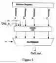
A command multiplication scheme is described in which CAD information provided by the low-speed BIST is used as a “seed” set for the generation of high-speed CAD patterns output to the memory. Specifically, the CMX described here takes seed CAD information from a BIST operating at a frequency, fBIST, and generates n sets of CAD data. Each generated CAD set is then output in turn to a memory system at a frequency that is equal to fBIST×n.
The CMX's CAD generation is accomplished by modifying the seed set based on the contents of previously loaded registers or previously set input signals. The modification can be anything from combining the seed set in a bit-wise fashion with the bits of a directive register through a logic unit (LU) to the addition of an offset using an arithmetic-logic unit (ALU). In the case of the latter, generating an address in a non-bit-wise manner is particularly important for simulating a worst-case noise condition in a multi-bank operation.
This invention is also directed to support multiple address generation from a common seed address using different address offsets for each address port. Generating multiple addresses is an important requirement when testing a memory with a concurrent refresh or multiple ports.
The inventive apparatus described may also be used to generate complex CAD patterns including non-bit-wise address sequences and multiple address generation. This results in more complete test coverage for both single and multiple port memories.
BRIEF DESCRIPTION OF DRAWINGSThe invention will be better understood from the following detailed description with reference to the drawings in which:
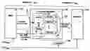
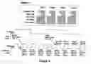
FIG. 1. A block diagram showing the interconnections of the BIST, CMX, and memory in accordance with the present invention.
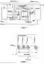
FIG. 2. A block diagram of a bit-wise command multiplier in accordance with a first embodiment of the present invention;
FIG. 3. A block diagram of a bit-wise command multiplier in accordance with a second embodiment of the present invention.
FIG. 4. A block diagram of a bit-wise command multiplier in accordance with a third embodiment of the present invention.
FIG. 5. A block diagram of a bit-wise command multiplier in accordance with a fourth embodiment of the present invention.
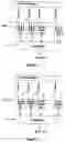
FIG. 6. An example of a timing diagram for CAD generation based on offsets where n equals 4; and
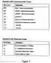
FIG. 7. Tables illustrating CMX command and data op codes.
DETAILED DESCRIPTION DETAILED DESCRIPTION OF INVENTIONFIG. 1 shows the flow of information from a low speed BIST 100, through the command multiplier (CMX) 110 to a memory system 120. During self-test, the BIST generates at low speed (fBIST) the seed set of CAD information, such as, commands, addresses, and data, which are inputs to the CMX. This seed set of CAD information is used to generate n sets of CAD information which are output to the memory at a high speed (fMEM), where
-
- fMEM=fBIST×n
- where: fMEM is the operating frequency of the memory,
- fBIST is the operating frequency of the BIST,
- n is the frequency multiplier.
This invention can be realized by several different configurations or embodiments shown in FIGS. 2, 3, 4, 5, and 6. Generally, configurations shown in FIGS. 2-5 generate the CAD sets in a bit-wise fashion by combining the seed CAD set with the contents of a directive register 130 through logic unit LU to a multiplexer 150. The configuration shown in FIG. 6 generates the “n” CAD sets based on offsets which are combined with the seed set in an ALU 140.
Note that the contents of the CMX registers 140 in the command multiplier 110, which could be directives or offset registers, switch at frequencies less than fBIST and typically will be static for an entire set of patterns generated by the BIST. As indicated in FIG. 1, these registers can be loaded via a dedicated, low-speed bus (REG_BUS) or by any other low speed means such as, for example, by an external tester.
Bit-Wise CAD Generation
For bit-wise generation n clocks of frequency fBIST are provided as inputs to the command multiplier shown in FIGS. 2-5, each of which is 360/n degrees out of phase from another. That is, if the i'th input clock is known as CLKin,i, then CLKin,i+1 is advanced by 360/n degrees from CLKin,i for all i=2 to n. The duty cycle of the input clocks should be 1/(2×n). Such clocks may be generated from an external tester, or from an on-chip DLL circuit.
The command multiplier 110 output clock is derived from the logical-or'ing function of all CLKin,i signals. Hence, the active edge of each CLKin,i signal identifies the start of the memory cycle. Thus, there will be “n” memory cycles associated with each BIST cycle.
With each CAD signal is associated from 1 to “n” directives that are stored in the directive registers. Each directive may consist of one or more bits. Directive registers switch at frequencies less than fBIST and typically will be static for an entire set of patterns generated by the BIST. The directives for a given CAD signal will be used to determine the output CAD set during each of the n embedded memory cycles that occur during a particular BIST cycle based on the output of the BIST and the state of the directive registers. Hence the output of the command multiplier is:
-
- CAD_out(i, m)=function(CAD_in(i), Directives(i), m)
- where
- CAD_out(i, m) is the i'th output CAD bit during the m'th of n embedded memory cycles associated with a BIST cycle,
- function is a logical function,
- CAD_in(i) is the i'th input CAD bit which is supplied by the BIST and may change each BIST cycle,
- Directives(i) are input directives associated with the i'th CAD bit. They are constant for one to many BIST cycles,
- m describes one of the n embedded memory cycles that make up one BIST cycle.
For example, there may be n directives, with each directive consisting of one bit. If the m'th directive bit is set in the m generator 160 that may be input to the multiplexer 150 or register 130, this could indicate that the CAD output is the inverse of the CAD input. If the directive bit is not set, then the CAD output is to equal the CAD input. Logically this is described as:
-
- CAD_out(i, m)=CAD_in(i) XOR Directive(i, m)
- where
- Directive(i, m) describes the m'th directive bit for the i'th CAD signal. Such a scheme can be implemented in a circuit as shown in FIG. 2.
An alternate embodiment is shown in FIG. 3, where the embedded memory cycle is an input to the logical function. Still other embodiments are shown in FIGS. 4 and 5.
In general, each Directive register(i, n) may be any number of bits. More bits may be used to enable more complicated or more flexible logical functions. Examples of some functions that may be performed using the directives are given below.
EXAMPLE 1As shown in the embodiment in FIG. 2 where each Directive(i, m) is a single bit.
-
- Logical function=Directive(i, m) XOR CAD_in(i)
As shown in the embodiment in FIG. 2 where each Directive is two bits,
-
- Directive_A(i,m) and Directive_B(i, m).
- Logical function=((Directive_A(i, m) AND Directive_B(i, m)) OR
- (Directive_A(i, m) XOR CAD_in(i))) AND
- (Directive_A(i, m) OR Directive_B(i, m))
As shown in the embodiment of FIG. 3 or 4 where “n” is four, and the m in-put to the command multiplier is encoded as a 2-bit word made of bits m1 and m2.
Also let each directive be one bit.
-
- Logical Function=CAD_in(i) XOR (Directive(i, m) XOR m1) XOR
- (Directive(i, m) XOR m2)
The behavior of Example 3 may be realized using the embodiment of FIG. 5. However, in this case, by utilizing the 2-bit encoding of the m variable, the number of directives can be reduced to two, with each directive consisting of 1-bit. In general, it is often possible to have fewer than m directives in this configuration.
-
- Logical function=CAD_in(i) XOR (Directive(i, 1) XOR m1) XOR
- (Directive(i, 2) XOR m2)
In addition to the circuitry described above, delays and pipeline stages must be added to assure that the CAD_out signals are synchronized with the output clock.
CAD Generation Based on Offsets
A memory which supports concurrent refresh (CCR) requires two bank addresses for each high-speed cycle, one for the command and one for the refresh. This means that, at the same time a READ, WRITE, or no-operation (NOP) command is being performed to bank address BA, a refresh is being performed to bank address RBA, which was generated using the same seed. Alternatively, separate seeds could be used to generate the n bank addresses for the command and CCR. A non-bit-wise addressing sequence may be accomplished by an offset addressing approach. As indicated above, the CMX 110 in FIG. 1 may include an offset address register and an ALU to generate the subsequent high-speed addresses. The detailed operation is described below.
Prior to the actual self-test, the BIST loads the n sets of CMX registers 130 via the REG_BUS. The register bits in the CMX contain the offset used to generate the subsequent high-speed addresses. When the BIST engine generates the seed CAD, the seed CAD information is captured by the CMX in synch with the low-speed clock (CLKBIST). The subsequent addresses for each command and refresh are then calculated by the adder circuit using the seed address and the corresponding address offset. The addresses are then launched to the memory in synch with the high-speed clock (CLKMEM).
The offset addresses may or may not be constant for each clock cycle. For example, by utilizing one seed bank address, BA, and two sets of n bank address offsets, OFFSET1 to OFFSETn for the command and OFFSETR1 to OFF-SETRn for refresh, the CMX can generate n high-speed bank addresses and n high-speed CCR addresses:
Command Addresses CCR Addresses
-
- BA+OFFSET1 BA+OFFSETR1
- BA+OFFSET2 BA+OFFSETR2
- . . .
- BA+OFFSETn BA+OFFSETRn
Because OFFSETi and OFFSETRi may be any integer, any addressing sequence can be generated. As discussed in the background, the most typical example is the address generation of b, b+1, b+2, . . . b+n, where b is any integer, which enables a worst-case noise pattern in a multi-bank operation. For example, a command operation and a CCR operation can be issued to two adjacent banks, b and b+1,simultaneously.
The number of OFFSET registers can be increased to allow the testing of multi-port memories.
Since the address space of a memory is finite, the result of the addition of a bank address seed and an offset will typically be truncated such that any binary carry that would produce an address that is outside of the address space of the memory is ignored.
Alternatively, the subsequent address generation may be determined by not only the seed and the contents of the CMX register's offset address, but also previous CAD seed inputs. For example, in order to perform a refresh on every other high-speed cycle, a counter could keep track of the number of refreshes so that the first eight refreshes to a 16 bank memory would be to the even banks, the next eight would be to odd banks, then even banks, then odd banks, and so on.
FIG. 6 illustrates another embodiment of CAD generation in which:
-
- n=4;
- the CMX generates the word address WA, the bank address BA, and the refresh bank address RBA by adding an offset (contained in the CMX registers) to the seed addresses provided by the BIST;
- only two data bits (DATA) are generated, one for all even data inputs of the memory, and one for all odd data inputs; these are generated based on op codes loaded into the CMX;
- the high-speed command information (CMD) is generated based on op codes loaded into the CMX.
The command and data op codes are provided in FIG. 7, Tables 1 and 2, respectively. While the invention has been described in terms of preferred embodiments, those skilled in the art will recognize that the invention can be practiced with modifications within the spirit and scope of the amended claims.
Claims
1. A command multiplier that generates sets of command, address, and data inputs (CAD) from a seed set having a plurality of bits provided at a low frequency by a BIST, to an embedded memory at a high frequency, comprising:
a directive register;
a logic unit; and
a multiplexer for time-multiplexing n generated CAD sets to the memory system at a frequency n times greater than the frequency at which the seed CAD set is received.
2. The command multiplier of claim 1 wherein there are c directive registers corresponding to c seed CAD bits, each register having n directive bits corresponding to the n CAD sets to be generated; and
n logic units (LUs) corresponding to the n CAD sets to be generated, each LU taking as an input the i th bit of the seed CAD and one of the n bits from the i th directive register.
3. The command multiplier of claim 1 wherein there are c directive registers corresponding to c seed CAD bits, each register having n directive bits corresponding to the n CAD sets to be generated; and
n logic units (LUs) corresponding to the n CAD sets to be generated, each LU taking as an input the i th bit of the seed CAD, one of the n bits from the i th directive register, and the binary-encoded time interval, m.
4. The command multiplier of claim 1 wherein there are c directive registers corresponding to c seed CAD bits, each register having n directive bits corresponding to the n CAD sets to be generated; and
n logic units (LUs) corresponding to the n CAD sets to be generated, each LU taking as an input the i th bit of the seed CAD, one of the n bits from the i th directive register, and a binary-encoded value corresponding to its directive bit input.
5. A command multiplier that generates multiple sets of command, address, and data inputs (CAD) from a seed CAD set having a plurality of bits provided at a low frequency to a memory system at a high frequency, comprising:
c directive registers corresponding to c seed CAD bits, each register having one or more directive bits;
a logic unit (LU) taking as an input the i th bit of the seed CAD, all of the bits from the i th directive register, and a binary-encoded time interval, m; and
a multiplexer for time-multiplexing n generated CAD sets to the memory system at a frequency n times greater than the frequency at which the seed CAD set is received;
6. A command multiplier that generates multiple sets of command, address, and data inputs (CAD) from a seed CAD set having a plurality of bits provided at a low frequency to a memory system at a high frequency, comprising:
a register;
an arithmetic logic unit (ALU); and
a multiplexer for time-multiplexing n generated CAD sets to the memory system at a frequency n times greater than the frequency at which the seed CAD sets are received.
7. The command multiplier of claim 6 which includes address offset registers corresponding to the n CAD sets to be generated, each contents of which is added to the corresponding seed address by the ALU to generate one of the n output addresses.
8. The command multiplier of claim 6 which includes opcode registers corresponding to the n CAD sets to be generated, each contents of which is combined with the corresponding seed CAD control signals to generate one of the n of that control signal.
9. A method for generating multiple sets of command, address, data inputs (CAD) from a seed CAD set having a plurality of bits provided by a BIST at low speed fBIST to a memory system at a higher speed fMEM comprising the steps of:
Loading a command multiplier register from the BIST;
ending the seed CAD set from the BIST to a logic block to generate n CAD sets; and
providing the n CAD sets to a multiplexer to send the CAD sets to the memory system at fMEM.
10. The method of claim 9 wherein the logic block is either a logic unit or an ALU.
Images & Drawings included:
Sources:
- United States Patent and Trademark Office - verify current appl. status at the USPTO↗
Recent applications in this class:
- » 20240120016 2024-04-11
At-speed test of functional memory interface logic in devices - » 20230035157 2023-02-02
Logic built-in self-test of an electronic circuit - » 20210335435 2021-10-28
JTAG BASED ARCHITECTURE ALLOWING MULTI-CORE OPERATION - » 20210327525 2021-10-21
AT-SPEED TEST OF FUNCTIONAL MEMORY INTERFACE LOGIC IN DEVICES - » 20210319841 2021-10-14
Systems and methods for detecting and configuring lanes in a circuit system - » 20190272886 2019-09-05
Integrated characterization vehicles for non-volatile memory cells - » 20190156908 2019-05-23
Enabling high at-speed test coverage of functional memory interface logic by selective usage of test paths - » 20190043601 2019-02-07
Built-in-self-test circuits and methods using pipeline registers - » 20180322937 2018-11-08
Apparatuses and methods including nested mode registers - » 20140026005 2014-01-23
Macro and command execution from memory array
Recent applications for this Assignee:
- » 20250294045 2025-09-18
THREAT POLICY FINE-TUNING BASED ON THE VULNERABILITY OF A SUBNET AS A SOURCE OF A MALICIOUS ATTACK - » 20250294041 2025-09-18
DEVICE POPULATION ANOMALY DETECTION - » 20250292574 2025-09-18
SCENE PARSING - » 20250292026 2025-09-18
A GENERATIVE ARTIFICIAL INTELLIGENCE COMMENTARY - » 20250291689 2025-09-18
MACHINE LEARNING MODEL TRAINING TO ASSIST IN SYSTEM DEBUG - » 20250287215 2025-09-11
PORTABLE MEDIA GEOFENCE AND DEVICE PAIRING SECURITY - » 20250285610 2025-09-11
RECIPIENT-SPECIFIC VOICE TONE ADJUSTMENT IN TELEPHONY - » 20250284728 2025-09-11
CONTEXT LARGE LANGUAGE MODEL OUTPUT EXPLANATION - » 20250278669 2025-09-04
COUNTERFACTUALS WITH FEATURE PREFERENCES FOR CONSISTENT AND DIVERSE EXPLANATIONS - » 20250274345 2025-08-28
MULTI-LAYER EDGE ARCHITECTURE SIMULATION