Method of manufacturing a sealed electronic module
US20050200045A1
2005-09-15
10/800,959
2004-03-15
✅ Patent granted
US 7,118,646 B2
2006-10-10
-
-
Justin Fischer
2024-09-29
Abstract:
A sealed electronic module is manufactured by forming a housing that is open at one end, dispensing a first quantity of potting material into the housing via the open end, inserting a circuit board and electrical connector assembly into the housing so that the inboard end of the circuit board is immersed in the potting material, and dispensing a second quantity of potting material into an area bridging the connector assembly and the housing. When cured, the first quantity of potting material attaches the inboard end of the circuit board to the housing, and the second quantity of potting material attaches the connector to the housing and environmentally seals the module.
Assignee:
- DELPHI TECHNOLOGIES, INC. 3,274 🇺🇸 TROY, MI, United States
Interested in similar patents?
Get notified when new applications in this technology area are published.
Classification:
H05K5/064 » CPC main
Casings, cabinets or drawers for electric apparatus; Hermetically-sealed casings sealed by potting, e.g. waterproof resin poured in a rigid casing
H05K5/064 » CPC main
Casings, cabinets or drawers for electric apparatus; Hermetically-sealed casings sealed by potting, e.g. waterproof resin poured in a rigid casing
B60R16/0239 » CPC further
Electric or fluid circuits specially adapted for vehicles and not otherwise provided for; Arrangement of elements of electric or fluid circuits specially adapted for vehicles and not otherwise provided for electric constitutive elements for transmission of signals between vehicle parts or subsystems Electronic boxes
H05K3/284 » CPC further
Apparatus or processes for manufacturing printed circuits; Secondary treatment of printed circuits; Applying non-metallic protective coatings for encapsulating mounted components
H05K3/284 » CPC further
Apparatus or processes for manufacturing printed circuits; Secondary treatment of printed circuits; Applying non-metallic protective coatings for encapsulating mounted components
H05K5/0039 » CPC further
Casings, cabinets or drawers for electric apparatus provided with connectors and printed circuit boards [PCB], e.g. automotive electronic control units having a tubular housing wherein the PCB is inserted longitudinally
H05K5/0039 » CPC further
Casings, cabinets or drawers for electric apparatus provided with connectors and printed circuit boards [PCB], e.g. automotive electronic control units having a tubular housing wherein the PCB is inserted longitudinally
H05K7/1417 » CPC further
Constructional details common to different types of electric apparatus; Mounting supporting structure in casing or on frame or rack having securing means for mounting boards, plates or wiring boards
H05K7/1417 » CPC further
Constructional details common to different types of electric apparatus; Mounting supporting structure in casing or on frame or rack having securing means for mounting boards, plates or wiring boards
H05K7/142 » CPC further
Constructional details common to different types of electric apparatus; Mounting supporting structure in casing or on frame or rack having securing means for mounting boards, plates or wiring boards Spacers not being card guides
H05K7/142 » CPC further
Constructional details common to different types of electric apparatus; Mounting supporting structure in casing or on frame or rack having securing means for mounting boards, plates or wiring boards Spacers not being card guides
H05K7/20463 » CPC further
Constructional details common to different types of electric apparatus; Modifications to facilitate cooling, ventilating, or heating characterised by the heat transfer by conduction from the heat generating element to a dissipating body; Inner thermal coupling elements in heat dissipating housings, e.g. protrusions or depressions integrally formed in the housing the coupling element being an additional piece, e.g. thermal standoff Filling compound, e.g. potted resin
H05K3/361 » CPC further
Apparatus or processes for manufacturing printed circuits; Assembling printed circuits with other printed circuits Assembling flexible printed circuits with other printed circuits
H05K3/361 » CPC further
Apparatus or processes for manufacturing printed circuits; Assembling printed circuits with other printed circuits Assembling flexible printed circuits with other printed circuits
H05K2201/10189 » CPC further
Indexing scheme relating to printed circuits covered by; Details of components or other objects attached to or integrated in a printed circuit board; Types of components Non-printed connector
H05K2201/10189 » CPC further
Indexing scheme relating to printed circuits covered by; Details of components or other objects attached to or integrated in a printed circuit board; Types of components Non-printed connector
H05K2201/10977 » CPC further
Indexing scheme relating to printed circuits covered by; Details of components or other objects attached to or integrated in a printed circuit board; Details of electrical connections of non-printed components, e.g. special leads; Other details of electrical connections Encapsulated connections
B32B37/00 IPC
Methods or apparatus for making layered products; Treatment of the layers or of the layered products
B32B37/00 IPC
Methods or apparatus for laminating, e.g. by curing or by ultrasonic bonding
H01L21/54 IPC
Processes or apparatus adapted for the manufacture or treatment of semiconductor or solid state devices or of parts thereof; Manufacture or treatment of semiconductor devices or of parts thereof the devices having at least one potential-jump barrier or surface barrier, e.g. PN junction, depletion layer or carrier concentration layer; Assembly of semiconductor devices using processes or apparatus not provided for in a single one of the subgroups - , e.g. sealing of a cap to a base of a container Providing fillings in containers, e.g. gas fillings
Description
TECHNICAL FIELDThe present invention relates to the manufacture of a sealed electronic module including a circuit board/connector assembly and a housing open at one end.
BACKGROUND OF THE INVENTIONIn the manufacture of electronic modules, various electronic components are mounted on a printed circuit board, connector terminals are soldered to a marginal portion of the circuit board, and the assembly is packaged in a plastic or metal housing. Usually, some provision is made for affixing the circuit board to the inner periphery of the housing, and the housing closes around the circuit board, with the connector pins protruding through the housing to enable electrical signal transmission to and from the module. In applications where the module has to be environmentally sealed, it is desirable to minimize the length and number of sealing surfaces. Theoretically, the sealing surfaces can be minimized by forming the housing as a single part with one opening through which the circuit board/connector assembly is inserted, but such an approach makes it difficult to attach the circuit board to the inner periphery of the housing since the interior of the housing is inaccessible after insertion of the circuit board/connector assembly. Alternatively, the entire housing may be filled with a potting material such as epoxy, but that is undesirable for several reasons, including cost, weight and the inadvisability of coating certain electronic components with potting material. Accordingly, what is needed is an improved method of manufacturing a sealed electronic module where the enclosed circuit board is securely attached to the inner periphery of the housing.
SUMMARY OF THE INVENTIONThe present invention is directed to the manufacture of an electronic module including a circuit board/connector assembly and a housing that is open at one end, where potting material is used to mechanically secure the circuit board to the housing and to provide an environmental seal at the open end of the housing. The empty housing is positioned so that its open end is facing upward, and a first quantity of potting material is dispensed into the housing. The circuit board/connector assembly is then inserted into the housing, immersing the inboard end of the circuit board into the potting material. The connector includes a cover that conforms to the inner periphery of the housing, forming an annular pocket at the open end of the housing, and a second quantity of potting material is then dispensed into the annular pocket. When cured, the first quantity of potting material attaches the inboard end of the circuit board to the inner periphery of the housing, and the second quantity of potting material attaches the connector to the housing and environmentally seals the module.
BRIEF DESCRIPTION OF THE DRAWINGSThe present invention will now be described, by way of example, with reference to the accompanying drawings, in which:—
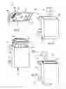
FIGS. 1A-1D illustrate the manufacturing method of this invention. FIG. 1A depicts a circuit board/connector assembly, FIG. 1B depicts a step of dispensing a first quantity of potting material into the open end of a housing; FIG. 1C depicts insertion of the circuit board/connector assembly of FIG. 1A into the housing of FIG. 1B; and FIG. 1D depicts a step of dispensing a second quantity of potting material into a pocket formed at the open end of the housing.
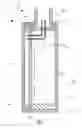
FIG. 2 is a cross-sectional view of an electronic module manufactured according to this invention.
DESCRIPTION OF THE PREFERRED EMBODIMENTThe manufacturing method of the present invention is disclosed in the context of an automotive electronic module such as a Sensing and Diagnostic Module (SDM) for deploying supplemental restraints in a severe crash event. In such an application, the enclosed circuit components 14 include acceleration-responsive sensors, and the circuit board 12 has to be securely attached to the inner periphery of the housing 18 to ensure that the sensors operate correctly. Of course, similar requirements occur in other applications as well, and the manufacturing method applies to sealed electronic modules per se, whether automotive or non-automotive.
Referring to FIG. 1A, the reference numeral 10 generally designates a circuit board/connector assembly, including a printed circuit board 12 supporting a number of electronic components 14, and a connector assembly 16. The connector assembly 16 is attached to the outboard end of the circuit board 12, and the components 14 may be distributed on the circuit board 12 in any convenient manner, except for a marginal portion 12a that includes the inboard end 12b of circuit board 12. The connector assembly 16 includes a plastic base plate 16a, a plastic header box 16b, and a number of metal connector pins 16c passing through the base plate 16a. The connector assembly 16 is preferably manufactured by an insert molding process so that the material of base plate 16a seals around the connector pins 16c. The leftward extending (outboard) ends of the pins 16c are disposed within the header box 16b (as seen in the cross-sectional view of FIG. 2) for attachment to a complementary electrical connector (not shown); and the rightward extending (inboard) ends of the pins 16c are bent toward the circuit board 12 for attachment thereto. Typically, the pins 16c extend through plated openings formed in the circuit board 12, and are soldered in place to both electrically and mechanically connect the circuit board 12 to the connector assembly 16.
In FIGS. 1B, 1C and 1D, the reference numeral 18 generally designates a housing for enclosing the circuit board/connector assembly 10. The housing 18 is preferably formed of plastic, and includes integral mounting tabs 18a for securing the completed electronic module to a support structure such as a vehicle frame element. The housing 18 is closed on all sides and one end, and is oriented so that the open end 18b is pointed upward as shown. The housing 18 is dimensioned so as to freely receive the circuit board/connector assembly 10 of FIG. 1A, with the inner periphery of the housing generally conforming to the circumferential periphery of the connector assembly base plate 16a.
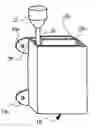
As shown in FIG. 1B, a dispensing nozzle 22 is positioned over the open end 18b of housing 18, and first quantity of potting material 20 is dispensed into bottom of housing 18. The potting material 20 fills the interior volume of housing 18 to a level such as shown by the broken line 24. The circuit board/connector assembly 10 is then inserted into the housing 18 as illustrated in FIG. 1C before the potting material 20 cures and hardens, immersing the marginal portion 12a of circuit board 12 into the potting material 20. This may be best seen in FIG. 2, which depicts a completed electronic module 26. As also shown in FIG. 2, the portion of the circuit board 12 on which the components 14 are mounted is not immersed in the potting material 20; this is important as it is inadvisable to coat certain electronic components with potting material.
When the circuit board/connector assembly 10 has been fully inserted into the housing 18, there is an annular pocket or cavity 28 through which the connector assembly header box 16b extends. Referring to FIGS. 1D and 2, the cavity 28 is defined by the connector assembly base plate 16a and header box 16b and the inner periphery of the housing 18 above the base plate 16a. At this point, the dispensing nozzle 22 is positioned over the cavity 28 as illustrated in FIG. 1D, and a second quantity of potting material 30 is dispensed into the cavity 28, preferably filling the cavity volume as depicted in FIG. 2.
The last step of the process is to allow undisturbed curing of the first and second quantities of potting material 20, 30 so that the potting material hardens substantially where dispensed. Referring to FIG. 2, the first quantity of potting material 20 then effectively attaches the marginal portion 12a of the circuit board 12 to the inner periphery 18c of the housing 18, and the second quantity of potting material 30 forms a seal between the connector assembly 16 and the inner periphery 18c of the housing 18, environmentally sealing the module 26. The potting material 20 may be of the same formulation as the potting material 30, or a different formulation if desired. In any case, the potting material 20, 30 may be any commercially available potting (epoxy, for example) that has an initial free-flowing state, and that chemically cures to a hardened state.
In summary, the manufacturing method of the present invention results in a reliably sealed electronic module 26 where potting material is used both to seal the housing 18 and to secure an enclosed circuit board 12 to the inner periphery 18c of housing 18. Only a small overall amount of potting material is required, which contributes to low cost and low weight of the module 26. Also, the potting material 20 only comes into contact with the marginal portion 12a of the circuit board 12, and does not come into contact with the electrical components 14 mounted elsewhere on the circuit board 12.
While the method of the present invention has been described in reference to the illustrated embodiment, it will be recognized that various modifications will occur to those skilled in the art. For example, the housing 18 may have a shape other than rectangular, and so on. Accordingly, it will be understood that manufacturing methods incorporating these and other modifications may fall within the scope of this invention, which is defined by the appended claims.
Claims
1. A method of manufacturing a sealed module that houses a circuit board supporting one more electronic components, the method comprising the steps of:
mechanically and electrically attaching an electrical connector to a first end of the circuit board;
providing a housing open at only one end, said housing having an inner periphery shaped to accommodate said circuit board and said electrical connector;
orienting said housing with said one end facing upward, and dispensing a first quantity of potting material into said housing through said one end;
inserting said circuit board and attached electrical connector into the one end of said housing such that only a marginal portion of said circuit board including a second end of said circuit board opposite said first end is immersed into said first quantity of potting material;
sealing said electrical connector to the inner periphery of said housing; and
curing said first quantity of potting material to secure said circuit board to the inner periphery of said housing.
2. The method of claim 1, where said marginal portion of said circuit board is free of said electronic components so that said first quantity of potting material does not come into contact with said components.
3. The method of claim 1, including the steps of:
dispensing a second quantity of potting material onto an outboard surface of said connector; and
curing said second quantity of potting material to seal said electrical connector to the inner periphery of said housing.
4. The method of claim 3, including the steps of:
providing a base plate on said electrical connector that conforms to the inner periphery of said housing so as to create a pocket defined by said base plate and the inner periphery of said housing when said circuit board and attached electrical connector are inserted into the one end of said housing; and
dispensing said second quantity of potting material into said pocket.
Images & Drawings included:
Sources:
- United States Patent and Trademark Office - verify current appl. status at the USPTO↗
Similar patent applications:
- » 20050150875
Package sealing method, manufacturing method of electronic device modules, sealing apparatus, and packaged product - » 20050198819
Method of manufacturing a sealed electronic module - » 20160249474
Package structure of electronic modules with silicone sealing frame and the manufacturing method thereof - » 20060286845
Sealed fastenerless multi-board electronic module and method of manufacture
Recent applications in this class:
- » 20250169014 2025-05-22
ELECTRICAL DEVICE WITH POTTING MATERIAL - » 20250048578 2025-02-06
PRINTED CIRCUIT BOARD FOR AN AUTOMATION FIELD DEVICE - » 20240196556 2024-06-13
Electronics unit - » 20220330447 2022-10-13
ELECTRIC CIRCUIT BOARD AND POWER MODULE - » 20220061179 2022-02-24
Display panel bend reinforcement - » 20210352816 2021-11-11
Explosion proof feed-through - » 20210084785 2021-03-18
Electronic device - » 20200288594 2020-09-10
FLUID METER, ENERGY STORAGE DEVICE FOR A FLUID METER, AND METHOD - » 20200060035 2020-02-20
Heat dissipation in an electronic circuit and method - » 20190373749 2019-12-05
Power supply device with PCB positioning function and method for manufacturing the same
Recent applications for this Assignee:
- » 20190217428 2019-07-18
Mounting system for an ultrasonic-welding installation - » 20180351286 2018-12-06
Sealed electrical connector assembly and wire seal - » 20180292823 2018-10-11
Motion-characteristic based object classification for automated vehicle - » 20180275282 2018-09-27
Automated vehicle GPS accuracy improvement using V2V communications - » 20180247724 2018-08-30
Electrically conductive carbon nanotube wire having a metallic coating and methods of forming same - » 20180240569 2018-08-23
Metallic/carbon nanotube composite wire - » 20180157269 2018-06-07
Vision sensing compensation - » 20180123263 2018-05-03
Coaxial-cable-assembly, ferrule, and method of making the same - » 20180122243 2018-05-03
Automated vehicle cross-traffic detection system - » 20180120845 2018-05-03
Automated vehicle sensor control system