Fluorene-based compound and organic electroluminescent display device using the same
US20050221124A1
2005-10-06
11/097,182
2005-04-04
✅ Patent granted
US 7,737,627 B2
2010-06-15
-
-
D. Lawrence Tarazano | Brett A Crouse
2028-01-27
Abstract:
The present invention relates to an organic electroluminescent (OEL) compound that comprises at least one fluorene derivative and at least one carbazole derivative. The compound has good electrical properties, light emitting properties and charge transport ability, and thus is suitable as a host material suitable for fluorescent and phosphorescent dopants of all colors including red, green, blue, white, etc., and as a charge transport material. An OEL display device that uses an organic layer that includes the OEL compound has a high efficiency, a low voltage, a high luminance, and a long lifespan because it has superior current density.
Inventors:
- Young-kook KIM 46 🇰🇷 Suwon-si, South Korea
- Seung Gak YANG 22 🇰🇷 Suwon-si, South Korea
- Hee Yeon KIM 31 🇰🇷 Suwon-si, South Korea
- Seok Hwan HWANG 27 🇰🇷 Suwon-si, South Korea
- Seok-Jong Lee 17 🇰🇷 Suwon-si, South Korea
Assignee:
- SAMSUNG MOBILE DISPLAY CO., LTD. 525 🇰🇷 Yongin, South Korea
Interested in similar patents?
Get notified when new applications in this technology area are published.
Classification:
C09K11/06 » CPC main
Luminescent, e.g. electroluminescent, chemiluminescent materials containing organic luminescent materials
C07D209/88 » CPC further
Heterocyclic compounds containing five-membered rings, condensed with other rings, with one nitrogen atom as the only ring hetero atom; Ring systems containing three or more rings [b, c]- or [b, d]-condensed; Carbazoles; Hydrogenated carbazoles with hetero atoms or with carbon atoms having three bonds to hetero atoms with at the most one bond to halogen, e.g. ester or nitrile radicals, directly attached to carbon atoms of the ring system
C07D401/12 » CPC further
Heterocyclic compounds containing two or more hetero rings, having nitrogen atoms as the only ring hetero atoms, at least one ring being a six-membered ring with only one nitrogen atom containing two hetero rings linked by a chain containing hetero atoms as chain links
C07D403/12 » CPC further
Heterocyclic compounds containing two or more hetero rings, having nitrogen atoms as the only ring hetero atoms, not provided for by group containing two hetero rings linked by a chain containing hetero atoms as chain links
C07D403/14 » CPC further
Heterocyclic compounds containing two or more hetero rings, having nitrogen atoms as the only ring hetero atoms, not provided for by group containing three or more hetero rings
C07F5/027 » CPC further
Compounds containing elements of Groups 3 or 13 of the Periodic System; Boron compounds Organoboranes and organoborohydrides
C07F9/5728 » CPC further
Compounds containing elements of Groups 5 or 15 of the Periodic System; Phosphorus compounds; Heterocyclic compounds, e.g. containing phosphorus as a ring hetero atom having one nitrogen atom as the only ring hetero atom; Five-membered rings condensed with carbocyclic rings or carbocyclic ring systems
H01L51/006 » CPC further
Solid state devices using organic materials as the active part, or using a combination of organic materials with other materials as the active part; Processes or apparatus specially adapted for the manufacture or treatment of such devices, or of parts thereof; Selection of organic semiconducting materials, e.g. organic light sensitive or organic light emitting materials; Macromolecular systems with low molecular weight, e.g. cyanine dyes, coumarine dyes, tetrathiafulvalene; Amine compounds having at least two aryl rest on at least one amine-nitrogen atom, e.g. triphenylamine comprising polycyclic condensed aromatic hydrocarbons as substituents on the nitrogen atom
H01L51/0061 » CPC further
Solid state devices using organic materials as the active part, or using a combination of organic materials with other materials as the active part; Processes or apparatus specially adapted for the manufacture or treatment of such devices, or of parts thereof; Selection of organic semiconducting materials, e.g. organic light sensitive or organic light emitting materials; Macromolecular systems with low molecular weight, e.g. cyanine dyes, coumarine dyes, tetrathiafulvalene; Amine compounds having at least two aryl rest on at least one amine-nitrogen atom, e.g. triphenylamine comprising heteroaromatic hydrocarbons as substituents on the nitrogen atom
C09K2211/1007 » CPC further
Chemical nature of organic luminescent or tenebrescent compounds; Non-macromolecular compounds; Carbocyclic compounds Non-condensed systems
C09K2211/1014 » CPC further
Chemical nature of organic luminescent or tenebrescent compounds; Non-macromolecular compounds; Carbocyclic compounds bridged by heteroatoms, e.g. N, P, Si or B
C09K2211/1029 » CPC further
Chemical nature of organic luminescent or tenebrescent compounds; Non-macromolecular compounds; Heterocyclic compounds characterised by ligands containing one nitrogen atom as the heteroatom
C09K2211/185 » CPC further
Chemical nature of organic luminescent or tenebrescent compounds; Metal complexes of the platinum group, i.e. Os, Ir, Pt, Ru, Rh or Pd
H01L51/0067 » CPC further
Solid state devices using organic materials as the active part, or using a combination of organic materials with other materials as the active part; Processes or apparatus specially adapted for the manufacture or treatment of such devices, or of parts thereof; Selection of organic semiconducting materials, e.g. organic light sensitive or organic light emitting materials; Macromolecular systems with low molecular weight, e.g. cyanine dyes, coumarine dyes, tetrathiafulvalene aromatic compounds comprising a hetero atom, e.g.: N,P,S comprising only nitrogen as heteroatom
H01L51/0072 » CPC further
Solid state devices using organic materials as the active part, or using a combination of organic materials with other materials as the active part; Processes or apparatus specially adapted for the manufacture or treatment of such devices, or of parts thereof; Selection of organic semiconducting materials, e.g. organic light sensitive or organic light emitting materials; Macromolecular systems with low molecular weight, e.g. cyanine dyes, coumarine dyes, tetrathiafulvalene aromatic compounds comprising a hetero atom, e.g.: N,P,S; Polycyclic condensed heteroaromatic hydrocarbons comprising only nitrogen in the heteroaromatic polycondensed ringsystem, e.g. phenanthroline, carbazole
H01L51/0085 » CPC further
Solid state devices using organic materials as the active part, or using a combination of organic materials with other materials as the active part; Processes or apparatus specially adapted for the manufacture or treatment of such devices, or of parts thereof; Selection of organic semiconducting materials, e.g. organic light sensitive or organic light emitting materials; Coordination compounds, e.g. porphyrin; Transition metal complexes, e.g. Ru(II)polypyridine complexes comprising Iridium
H01L51/5012 » CPC further
Solid state devices using organic materials as the active part, or using a combination of organic materials with other materials as the active part; Processes or apparatus specially adapted for the manufacture or treatment of such devices, or of parts thereof specially adapted for light emission, e.g. organic light emitting diodes [OLED] or polymer light emitting devices [PLED] Electroluminescent [EL] layer
H01L51/5016 » CPC further
Solid state devices using organic materials as the active part, or using a combination of organic materials with other materials as the active part; Processes or apparatus specially adapted for the manufacture or treatment of such devices, or of parts thereof specially adapted for light emission, e.g. organic light emitting diodes [OLED] or polymer light emitting devices [PLED]; Electroluminescent [EL] layer Triplet emission
H01L51/5048 » CPC further
Solid state devices using organic materials as the active part, or using a combination of organic materials with other materials as the active part; Processes or apparatus specially adapted for the manufacture or treatment of such devices, or of parts thereof specially adapted for light emission, e.g. organic light emitting diodes [OLED] or polymer light emitting devices [PLED] Carrier transporting layer
Y10S428/917 » CPC further
Stock material or miscellaneous articles Electroluminescent
H05B33/14 » CPC further
Electroluminescent light sources; Light sources with substantially two-dimensional radiating surfaces characterised by the chemical or physical composition or the arrangement of the electroluminescent material, or by the simultaneous addition of the electroluminescent material in or onto the light source
C07D209/82 IPC
Heterocyclic compounds containing five-membered rings, condensed with other rings, with one nitrogen atom as the only ring hetero atom; Ring systems containing three or more rings [b, c]- or [b, d]-condensed Carbazoles; Hydrogenated carbazoles
C07C211/00 IPC
Compounds containing amino groups bound to a carbon skeleton
C07C15/27 IPC
Cyclic hydrocarbons containing only six-membered aromatic rings as cyclic parts; Polycyclic condensed hydrocarbons containing three rings
Description
CROSS REFERENCE TO RELATED APPLICATIONThis application claims the priority to and benefit of Korean Patent Application No. 10-2004-0022877, filed on Apr. 2, 2004 in the Korean Intellectual Property Office, the disclosure of which is incorporated herein in its entirety by reference.
BACKGROUND OF THE INVENTION1. Field of the Invention
The present invention relates to a fluorene-based compound and an organic electroluminescent (OEL) display device that uses the same. In particular, the present invention relates to an OtL compound that has a structure that comprises at least one fluorene derivative and at least one carbazole derivative. The present invention also relates to an OEL display device with an organic emission layer or a hole transport layer that includes the OEL compound.
2. Description of the Background
In general, an OEL display device (OEL device) has an anode, a hole transport layer (HTL), an emission layer (EML), an electron transport layer (ETL), and a cathode that are sequentially formed on a substrate. The HTL, the EML, and the ETL are organic thin films.
The OEL device with the structure described above operates as follows. When a voltage is applied to the anode and the cathode, holes injected from the anode migrate to the EML via the HTL. Meanwhile, electrons from the cathode are injected in the EML via the ETL. Carriers are recombined in the EML to generate excitons. When these excitons fall from an excited state to a ground state, they emit light in the EML, which forms an image. The light that is emitted when excitons drop to the ground state from a singlet excitation state is referred to as “fluorescence.” The light that is emitted when excitons drop to the ground state from a triplet excitation state is referred to as “phosphorescence.” Fluorescence with a probability of the singlet excitation state of 25% (triplet excitation state: 75%) has a low luminous efficiency, whereas phosphorescence using a singlet excitation state of 25% and a triplet excitation state of 75% can theoretically have an internal quantum efficiency of about 100%.
A green and red high-efficiency OEL device has been developed that uses Ir(ppy)3 and PtOEP which are phosphorescent pigments that have heavy elements Ir and Pt with a high spin-orbital coupling energy at their central positions as dopants. These pigments effectively emit light even in a triple state (phosphorescent) OEL. In this type of device, 4,4′-N,N′-dicarbazole biphenyl (CBP) is used as a host. CBP has a low glass transition temperature of 110° C. or less and is easily crystallized. Due to CBP's unstable properties, this OEL device has a short life span of only 150 hours or less and is thus unsuitable for commercial use.
SUMMARY OF THE INVENTIONThe present invention provides an organic light emitting compound having at least one fluorene derivative and at least one carbazole derivative as side chains. It is used as a host material because it has electrical stability, good charge transport ability, a high glass transition temperature, is capable of preventing crystallization, and is suitable for use with fluorescent dopants and phosphorescent dopants of all colors including red, green, blue and white colors.
The present invention also provides an OEL device that has improved efficiency, low voltage, high luminance and long lifespan due to superior current density that uses an organic layer that includes the host material described above.
Additional features of the invention will be set forth in the description which follows, and in part will be apparent from the description, or may be learned by practice of the invention.
The present invention provides a fluorene-based compound represented by Formula (1) below:
Z is represented by:
Ar is a substituted or unsubstituted aryl group or a group represented by Formula 2.
X is N, B or P. Y is a single bond, a substituted or unsubstituted C1-C30 alkylene group, a substituted or unsubstituted C6-C30 arylene group, or a substituted or unsubstituted C4-C30 heterocyclic group.
Each of R1, R2 and R3 is a hydrogen atom, a substituted or unsubstituted C1-C30 alkyl group, a substituted or unsubstituted C6-C30 aryl group, a substituted or unsubstituted C4-C30 heterocyclic group, or a substituted or unsubstituted C6-C30 condensed polycyclic group. The neighboring groups among R1, R2 and R3 are connected to each other to form a saturated or unsaturated carbon ring.
Each of R′ and R″ is a hydrogen, a hydroxy group, a substituted or unsubstituted C1-C30 alkyl group, or a substituted or unsubstituted C6-C30 aryl group.
The present invention also provides an OEL device that includes a pair of electrodes and an organic layer interposed between the electrodes, where the organic layer includes the above-described fluorene-based compound.
It is to be understood that both the foregoing general description and the following detailed description are exemplary and explanatory and are intended to provide further explanation of the invention as claimed.
BRIEF DESCRIPTION OF THE DRAWINGSThe accompanying drawings, which are included to provide a further understanding of the invention and are incorporated in and constitute a part of this specification, illustrate embodiments of the invention and together with the description serve to explain the principles of the invention.
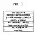
FIG. 1 is a schematic cross-sectional view of an OEL device of the present invention.
FIG. 2 is a graph illustrating the relationship between the voltage and the luminance of OEL devices prepared according to Example 1 of the present invention and Comparative Example 1.
FIG. 3 is a graph illustrating the relationship between the voltage and the luminance of OEL devices prepared according to Example 2 of the present invention and Comparative Example 2.
FIG. 4 is photoluminescence (PL) spectrum of OEL compounds according to the present invention.
DETAILED DESCRIPTION OF THE INVENTIONA fluorene-based compound represented by Formula (1) of the present invention has a high glass transition temperature (melting point) due to the presence of a rigid carbazole group in its structure. This improves its resistance to heat generated in an organic layer, between the organic layers, and/or between an organic layer and a metal electrode during electroluminescence and the resistance under a high temperature environment. Thus, when this compound is used as a hole transport layer, as an emission material of an OEL device, or as a host material of an emission layer, a high luminance and prolonged light emission are also possible.
In particular, a fluorene-based compound with at least two rigid carbazole groups can further improve the above effects. In addition, since the carbazole group improves an energy transition from a singlet excitation state to a triplet excitation state resulting in a smooth energy transfer from the host to the dopant, when the fluorine-based compound is used as a phosphorescent host for green and red phosphorescent dopants, a high efficiency and high luminance OEL device can be obtained.
The fluorene-based compound represented by Formula (1) has a fluorene derivative structure in its molecule which facilitates a singlet transition. Thus, when the fluorene-based compound is used in the emission layer, a high luminance is obtained due to increased fluorescence intensity. When the fluorene-based compound is used as a host for a fluorescent dopant and a phosphorescent dopant, a high luminance can also be obtained due to an increased energy transfer to the dopant.
The fluorene-based compound represented by Formula (1) can be used as an emission material, a hole transport material or a hole injection material.
Examples of the fluorene-based compound represented by Formula (1) include the following compounds represented by Formula (3), Formula (4), and Formula (5). These compounds are light emitting materials that have good light-emitting and hole transmission properties and may be used as a blue light emitting material, as green and red phosphorescent and fluorescent host materials, or as a hole transport material.
In Formulas (3)-(5), Ar is a substituted or unsubstituted aryl group or a group represented by Formula 2:
X is N, B or P. Each of Y and Yd is a single bond, or a substituted or unsubstituted C1-C30 alkylene group, a substituted or an unsubstituted C6-C30 arylene group or a substituted or unsubstituted C4-C30 heterocyclic group.
Each of R1, R2 and R3 is a hydrogen, a substituted or an unsubstituted C1-C30 alkyl group, a substituted or unsubstituted C6-C30 aryl group, a substituted or unsubstituted C4-C30 heterocyclic group, or a substituted or unsubstituted C6-C30 condensed polycyclic group. The neighboring groups among R1, R2 and R3 are connected to each other to form a saturated or unsaturated carbon ring.
Each of R′ and R″ is a hydrogen, a hydroxy group, a substituted or an unsubstituted C1-C30 alkyl group, or a substituted or unsubstituted C6-C30 aryl group.
In the above Formulas (3)-(5), the substituted or unsubstituted aryl group Ar may include, but is not limited to a phenyl group, an ethylphenyl group, an ethylbiphenyl group, o-, m- and p-fluorophenyl groups, a dichlorophenyl group, a dicyanophenyl group, a trifluoromethoxyphenyl group, o-, m- and p-tolyl groups, o-, m- and p-cumenyl groups, a mesityl group, a phenoxyphenyl group, a (α,α-dimethylbenzene) phenyl group, (N,N′-dimethyl)aminophenyl group, a (N,N′-diphenyl) aminophenyl group, a pentalenyl group, an indenyl group, a naphthyl group, a methylnaphthyl group, an anthracenyl group, an azrenyl group, a heptarenyl group, an acenaphthylenyl group, a phenarenyl group, a fluorenyl group, an anthraquinolyl group, a methylanthryl group, a phenanthryl group, a triphenylene group, a pyrenyl group, a crycenyl group, an ethyl-crycenyl group, a picenyl group, a perylenyl group, a chloroperylenyl group, a pentaphenyl group, a pentacenyl group, a tetraphenylene group, a hexaphenyl group, a hexacenyl group, a rubicenyl group, a coroneryl group, a trinaphthylenyl group, a heptaphenyl group, a heptacenyl group, a pyranthrenyl group, an ovarenyl group, a carbazolyl group, etc. Preferably, Ar is a phenyl group, a lower alkylphenyl group, a lower alkoxyphenyl group, a cyanophenyl group, a phenoxyphenyl group, a halophenyl group, a naphthyl group, a lower alkylnaphthyl group, a lower alkoxynaphthyl group, a cyanonaphthyl group, a halonaphthyl group, a fluorenyl group, a carbazolyl group, a lower alkylcarbazolyl group, a biphenyl group, a lower alkylbiphenyl group, a lower alkoxybiphenyl group, a thiophenyl group, an indolyl group or a pyridyl group. The lower alkyl and lower alkoxy groups preferably have 1 to 5 carbon atoms. More preferably, Ar may be a aryl group selected from a fluorenyl group, a carbazolyl group, a phenyl group, a naphthyl group and a phenanthrenyl group, an aromatic ring of which may be substituted by one to three, preferably one C1-C3 lower alkyl, C1-C3 lower alkoxy, cyano, phenoxy, phenyl or halogen atom.
Examples of compounds represented by Formulas (3) to (5) include the following compounds:
The fluorene-based compound represented by Formula (1) is prepared according to the following method where X is N.
Reaction scheme 1
Referring to the reaction scheme 1, brominated fluorene is reacted with Ar—XH2, and then reacted with Z containing iodide, such as Z-I, to obtain the compound represented by Formula (1). In the reaction, Z-I may be replaced with Z-Br, Z-Cl, etc., and brominated fluorene may be replaced with other halogenated fluorene, such as chlorinated fluorene.
A method of preparing an OEL device according to the present invention will now be described.
FIG. 1 is a cross-sectional view of a general OEL device.
First, a first electrode material with a high work function is coated on a substrate by a deposition method or a sputtering method to form a first electrode. Any substrate that is used in a conventional OEL device may be used, and a glass substrate or a transparent plastic substrate that is waterproof, has good mechanical strength, thermal stability, transparency, and surface softness, and can be easily handled is preferable. The first electrode material may be, for example, indium tin oxide (ITO), indium zinc oxide (IZO), tin oxide (SnO2), or zinc oxide (ZnO), which is transparent and has good conductivity.
A hole injection layer (HIL) may be formed on the first electrode by vacuum evaporation, spin-coating, cast, Langmuir-Blodgett (LB), etc. Vacuum evaporation is preferable because it provides a uniform layer and hardly produces a pin hole. When the HIL is formed by vacuum evaporation, the evaporation conditions vary according to a compound used as the HIL material, the desired structure and thermal property of the HIL, but generally have an evaporation temperature of 50 to 500° C., a vacuum pressure of 10−8 to 10−3 torr, an evaporation rate of 0.01 to 100 ÅÅ/sec, and a layer thickness is selected to be in the range of 10 Å to 5 μm.
The HIL material is not particularly restricted and may include phthalocyanine compounds, such as copper phthalocyanine disclosed in U.S. Pat. No. 4,356,429, the disclosure of which is incorporated herein in its entirety by reference, or a starburst type amine derivative, such as TCTA, m-MTDATA, or m-MTDAPB [Advanced Material, 6, p. 677 (1994)].
A hole transport layer (HTL) is formed on the HIL by vacuum evaporation, spin coating, cast, LB, etc. Again, vacuum evaporation is preferable because it provides a uniform layer and hardly produces a pin hole. When the HTL is formed by the vacuum evaporation, the evaporation conditions vary according to a compound used, but are similar to the evaporation conditions of the HIL. A HTL material is not particularly restricted and may be the fluorene-based compound by the represented by Formula (1) according to the present invention or any known material that is used in the HTL. For example, carbazole derivatives, such as N-phenylcarbazole and polyvinylcarbazole, or conventional amine derivatives having an aromatic condensed ring, such as N,N′-bis(3-methylphenyl)-N,N′-diphenyl-[1,1 -biphenyl]-4,4′-diamine (TPD) and N,N′-di(naphthalen-1-yl)-N,N′-diphenyl benzidine (α-NPD) may be used as the HTL material.
An emission layer (EML) is formed on the HTL by vacuum evaporation, spin coating, cast, LB, etc. Again, vacuum evaporation is the preferred method because it provides a uniform layer and hardly produces a pin hole. When the EML is formed by the vacuum evaporation, the evaporation conditions vary according to the compound used, but are similar to the evaporation conditions of the HIL. An EML material is not particularly restricted and the compound represented by Formula (1) of the present invention is used alone or as a host.
When the compound represented by Formula (1) is used as the light-emitting host, the EML may be formed using a phosphorescent or fluorescent dopant together. IDE102 or IDE105 available from Idemitsu may be used as the fluorescent dopant and Ir(ppy)3 (fac tris(2-phenylpyridine) iridium) (green) or FIrpic (iridium(III)bis[4,6-di-(fluorophenyl)-pyridinato-N,C2′] picolinate) (blue) is used as the phosphorescent dopant.
A red phosphorescent dopant RD61 etc. available from UDC may also be vacuum co-deposited (doped). The concentration of the dopant is not particularly restricted, but may be 0.01 to 15 parts by weight based on 100 parts by weight of a host. When the concentration of the dopant is less than 0.01 parts by weight, it does not sufficiently impart color to the EML. When the concentration of the dopant is greater than 15 parts by weight, an undesirable concentration quenching occurs, which sharply reduces the efficiency.
Further, when the phosphorescent dopant is used in the EML, a hole-blocking material is deposited on the EML by vacuum evaporation or spin-coating to form a hole-blocking layer (HBL), in order to prevent a triplet exciton or a hole from diffusing into an electron transport layer. The hole-blocking material is not particularly restricted and may be any known material that is used as the hole blocking material. For example, an oxadiazole derivative, a triazole derivative, a phenanthroline derivative, or a hole-blocking material described in Japanese Patent Laid-Open Publication No. Hei 11-329734 A1, the disclosure of which is incorporated herein in its entirety by reference, may be used. Typically, Balq represented by the following formula, phenanthrolines (e.g. BCP available from UDC), etc. is used:
An electron transport layer (ETL) is formed on the EML by vacuum evaporation, spin-coating or cast, preferably vacuum evaporation. An ETL material is not particularly restricted as long as it stably transports electrons injected from a cathode. A quinoline derivative, in particular, aluminum tris(8-quinolinorate) (Alq3) may be used as the ETL material. An electron injection layer (EIL) which facilitates injection of electrons from the cathode may be deposited on the ETL. An EIL material is not particularly restricted, but may be LiF, NaCl, CsF, Li2O, BaO, etc. The deposition conditions of the HBL, ETL, EIL vary according to compounds used, but are similar to the conditions for the HIL.
Finally, a metal is deposited on the EIL using vacuum evaporation or sputtering to form a second electrode. The metal that forms the second electrode may be a metal, an alloy, an electroconductive compound or a mixture thereof that has a low work function, for example, Li, Mg, Al, Al—Li, Ca, Mg—In, Mg—Ag, etc. Furthermore, to obtain a top-emission device, a transmittance type cathode composed of ITO or IZO may be used.
The OEL device according to the present invention may include one or two intermediate layers in addition to the anode (first electrode), the HIL, the HTL, the EML, the ETL, the EIL, and the cathode illustrated in FIG. 1. Even though the HIL, the EIL and the HBL are not required, they can improve the luminous efficiency.
The present invention will be described in greater detail with reference to the preferable Synthesis Examples of the compound represented by Formula 1 that has at least one fluorene derivative and at least one carbazole derivative as side chains. The following examples are for illustrative purposes and are not intended to limit the scope of the invention.
Example 1Reaction Scheme 2
Synthesis of an Intermediate A
3.344 g (20 mmol) of carbazole was added to 40 mL of DMPU (1,3-dimethyl-3,4,5,6-tetrahydro-2(1H)-pyrimidinone), and then 0.761 g (4 mmol) of CuI, 11.057 g (80 mmol) of K2CO3, and 0.1 g (4 mmol) of 18-crown-6 were added thereto. Next, the mixture was stirred at 170° C. for 20 hours, cooled to room temperature, and distilled under a reduced pressure to remove the solvent. The resultant was dissolved in 100 mL of dichloromethane and was washed with water several times. The washed dichloromethane layer was dried on MgSO4 and dried under a reduced pressure to obtain a crude product. The crude product was separated and purified by column chromatography on silica gel and recrystallized from hexane to obtain 3.28 g (yield 67%) of the intermediate A as a solid.
Synthesis of an Intermediate B
2.433 g (10 mmol) of the intermediate A was added to 100 mL of 80% acetic acid, and then 1.357 g (5.35 Mmol) of I2 and 0.333 g (1.46 mmol) of H5IO6 were is added thereto in a solid phase. Next, the mixture was stirred under a N2 atmosphere at 80° C. for 2 hours. After the reaction was completed, the resulting product was extracted with ethyl ether (50 mL) three times to collect organic layers. The collected organic layer was dried on MgSO4 and the solvent was evaporated to obtain a residue. The residue was separated and purified by column chromatography on silica gel to obtain 3.23 g (yield 87%) of the intermediate B.
Reaction Scheme 3
Synthesis of an Intermediate C
13 g (53 mmol) of 2-bromofluorene was dissolved in 60 mL of acetic acid. 60 g (200 mmol) of sodium bichromate was slowly added to the solution at 0° C. After 12 hours, 200 mL of distilled water was added to the mixture and thoroughly stirred. The resulting yellow solid was filtered and dried to obtain 10 g of the intermediate C (yield 78%).
Synthesis of an Intermediate D
8 g (31.6 mmol) of the intermediate C was dissolved in 60 mL of THF. Next, 38 mL (38 mmol) of 1 M phenylmagnesium bromide was slowly added to the solution at −78° C. After 2 hours, the mixture was heated to room temperature and stirred at the same temperature for 5 hours. The resulting was diluted with 50 mL of an aqueous ammonium chloride solution and was extracted three times with ethyl acetate (40 mL) to form organic layers. The collected organic layer was dried on MgSO4 and the solvent was evaporated to obtain a residue. The residue was separated and purified by column chromatography on silica gel to obtain 10 g (yield 95%) of the intermediate D.
The structure of the intermediate D was identified by 1H-NMR ((CDCl3, 400MHz) δ (ppm) 7.64 (d, 1H), 7.54-7.47 (m, 2H), 7.44 (d, 1H), 7.39-7.33 (m, 7.23 (m, 5H), 2.46 (s, 1H)).
Synthesis of an Intermediate E
10 g (30 mmol) of the intermediate D was dissolved in 60 mL of benzene and 2.4 mL (45 mmol) of concentrated sulfuric acid that is diluted with a small amount of benzene. The mixture was stirred at 80° C. for 5 hours and benzene was evaporated to obtain a residue. The residue was made to pH 7 using a 1M aqueous sodium hydroxide solution, and then extracted three times with 40 mL of ethyl acetate. The collected organic layer was dried on MgSO4 and the solvent was evaporated to obtain a residue. The residue was separated and purified by column chromatography on silica gel to obtain 6 g (yield 50%) of the intermediate E.
Synthesis of an Intermediate F
460 mg (1.16 mmol) of the intermediate E was dissolved in 5 mL of THF and. Next, 0.61 mL (1.5 mmol) of a 2.5 M n-butyl lithium solution in n-hexane was added dropwise to the solution at −78° C. Then, the mixture was stirred for 2 hours. 0.33 mL (2.9 mmol) of trimethyl borate was added to the reaction and stirred at the same temperature for 3 hours and then at room temperature for 12 hours. A 12 M HCl aqueous solution was added to the resulting mixture and stirred at room temperature for 2 hours to form a solution with a pH of 1. Then, the mixture was made to be pH of 14 with a 4 M NaOH aqueous solution and three times extracted with diethyl ether (10 mL) to collect organic layers. The collected organic layer was dried on MgSO4 and the solvent was evaporated to obtain a residue. The residue was separated and purified by column chromatography on silica gel to obtain 345 mg (yield 82%) of the intermediate F as a white solid.
Synthesis of an Intermediate G
344 mg (0.95 mmol) of the intermediate F and 560 mg (2.37 mmol) of 1,4-dibromobenzene were dissolved in 10 mL of THF. Next, 22 mg (0.02 mmol) of palladium tetrakistriphenylphosphine was added to the solution. Then, a solution of 660 mg (4.8 mmol) of K2CO3 in 8 mL of distilled water was added to the mixture and stirred at 75° C. for 12 hours.
The mixture was extracted three times with 15 mL of ethyl acetate to collect organic layers. The collected organic layer was dried on MgSO4 and the solvent was evaporated to obtain a residue. The residue was separated and purified by column chromatography on silica gel to obtain 2.90 mg (yield 65%) of the intermediate G. The structure of the intermediate G was identified by 1H NMR (1H-NMR (CDCl3, 400MHz) δ (ppm) 7.79 (dd, 1H), 7.77 (dd, 1H), 7.57 (d, 1H), 7.54 (dd, 1H), 7.49 (dd, 2H), 7.42-7.37 (m, 3H), 7.35 (dd, 1H), 7.27 (dt, 1H), 7.25-7.19 (m, 10H)) and 13C-NMR (13C-NMR (CDCl3, 100 MHz) δ (ppm) 152.0, 151.8, 145.8, 140.2, 139.8, 139.6, 139.5, 131.8, 128.7, 128.3, 128.1, 127.9, 127.6, 126.7, 126.5, 126.3, 124.7, 120.5, 120.3, 65.6).
Reaction Scheme 4
Synthesis of an Intermediate K
340 mg (0.856 mmol) of the intermediate E and 142 mg (1.2 mmol) of 4-aminobenzonitrile were dissolved in 5 mL of toluene and 0.144 g (1.5 mmol) of t-BuONa, 0.018 g (0.02 mmol) of Pd(dba)2 and 0.004-0.006 g (0.02-0.03 mmol) of(t-Bu)3P were added thereto, and then stirred at 80° C. for 5 hours. The reaction was extracted three times with 20 mL of ethyl ether to collect organic layers. The collected organic layer was dried on MgSO4 and the solvent was evaporated to obtain a residue. The residue was separated and purified by column chromatography on silica gel to obtain 0.27 g (yield 73%) of the intermediate K.
Synthesis of the Compound 14
267 mg (0.614 mmol) of the intermediate K and 0.332 g (0.9 mmol) of the intermediate B were dissolved in 10 mL of toluene. Next, 0.144 g (1.5 mmol) of t-BuONa, 0.018 g (0.02 mmol) of Pd(dba)2 and 0.004-0.006 g (0.02-0.03 mmol) of (t-Bu)3P were added to the solution and then stirred at 90° C. for 6 hours.
The reaction mixture was extracted three times with 30 mL of ethyl ether to collect organic layers. The collected organic layer was dried on MgSO4 and the solvent was evaporated to obtain a residue. The residue was separated and purified by column chromatography on silica gel to obtain 0.236 g (yield 57%) of the compound 14. The structure of the compound 14 was identified by 1H-NMR(1H-NMR (CDCl3, 400 MHz) δ (ppm) 7.97 (d, 1H), 7.90 (d,1H), 7.69 (d, 1H), 7.65 (d, 1H), 7.60 (d, 2H), 7.56 (dd, 2H), 7.48 (m, 1H), 7.40 (d, 2H), 7.35 (m, 6H), 7.24 (m, 3H), 7.16 (m, 10H), 7.11 (dd, 1H), 6.93 (d, 2H))
EXAMPLE 1A ITO glass substrate (Corning Co, surface resistance: 15 Ω/cm2, thickness: 1200 Å) was cut to a size of 50 mm×50 mm×0.7 mm to form an anode. Next the substrate was ultrasonically cleaned in isopropyl alcohol and pure water each for 5 minutes, then irradiated with UV light for 30 minutes, exposed to ozone, and washed. Then, the glass substrate was placed on a vacuum evaporator.
IDE406 (available from Idemitsu) was vacuum evaporated on the glass is substrate to form an HIL having a thickness of 600 Å. Then, 4,4′-bis[N-(1-naphthyl)-N-phenylaamino]biphenyl (NPB) was vacuum evaporated to a thickness of 300 Å on the HIL to form an HTL.
Subsequently, a mixture of the compound 14 as a phosphorescent host and Ir(ppy)3 as a green phosphorescent dopant in a weight ratio of 93:7 was deposited on the HTL to form an EML with a thickness of 300 Å. Alq3 was deposited on the EML to form an ETL having a thickness of 300Å. LiF was deposited on the ETL to form an EIL having a thickness of 10 Å and Al was deposited on the EEL to form a cathode having a thickness of 3000 Å, thereby completing an OEL device.
A color coordinate, a luminance, luminous efficiency and the like of the OEL device were measured. As a result, it was found that the OEL device had a current density of 31.46 mA/cm2, a luminance of 2,000 cd/m2, a color coordinate of (0.30, 0.60), and a luminous efficiency of 6.5 cd/A at a DC voltage of 6V.
COMPARATIVE EXAMPLE 1An OEL device was prepared in the same manner as in Example 1, except that a mixture of CBP as a phosphorescent host and Ir(ppy)3 as a green phosphorescent dopant at a weight ratio of 93:7 was deposited on the HTL to form an EML.
A color coordinate, a luminance, luminous efficiency and the like of the OEL device were measured. As a result, it was found that the OEL device had a current density of 5.17 mA/cm2, a luminance of 1,168 cd/m2, a color coordinate of (0.30, 0.60), and a luminous efficiency of 22.4 cd/A at a DC voltage of 6 V.
It can be seen from the above results that when the compound 14 according to the present invention is used as the green phosphorescent host, the turn-on voltage was lowered by as much as 1 V due to a remarkable improvement in charge transport ability and the significant increase in luminance at the same turn-on voltage. FIG. 2 shows that Example 1 using the compound 14 has a turn-on voltage that is lower than that of Comparative Example 1 and shows a higher luminance at the same turn-on voltage.
EXAMPLE 2A ITO glass substrate (Corning Co, surface resistance: 15 n/cm2, thickness: 1200 Å) was cut to a size of 50 mm×50 mm×0.7 mm to form an anode. Next, the substrate was ultrasonically cleaned in isopropyl alcohol and pure water each for 5 minutes, irradiated with UV light for 30 minutes, exposed to ozone, and washed. Then, the glass substrate was placed on a vacuum evaporator. IDE406 was vacuum evaporated on the glass substrate to form an HIL having a thickness of 600Å. Then, NPB was vacuum evaporated to a thickness of 300 Å on the HIL to form an HTL. Subsequently, a mixture of the compound 14 as a phosphorescent host and RD61 (available from UDC) as a red phosphorescent dopant at a weight ratio of 90:10 was deposited on the HTL to form an EML having a thickness of 300 Å.
Alq3 was then deposited on the EML to form an ETL with a thickness of 300 Å. LiF was deposited on the ETL to form an EIL having a thickness of 10 Å and Al was deposited on the EIL to form a cathode having a thickness of 3000 Å, thereby completing an OEL device.
A color coordinate, a luminance, luminous efficiency and the like of the OEL device were measured. As a result, it was found that the OEL device had a current density of 23.44 mA/cm2, a luminance of 1,979 cd/m2, a color coordinate of (0.62, 0.38), and a luminous efficiency of 8.44 cd/A at a DC voltage of 5 V.
COMPARATIVE EXAMPLE 2An OEL device was prepared in the same manner as in Example 1, except that a mixture of CBP as a phosphorescent host and RD61 as a red phosphorescent dopant at a weight ratio of 90:10 was deposited on the HTL to form an EML.
For the OEL device, a color coordinate, a luminance, luminous efficiency and the like were measured. As a result, it was found that the OEL device had a current density of 4.27 mA/cm2, a luminance of 423.3 cd/M2 , a color coordinate of (0.62, 0.38), and a luminous efficiency of 9.92 cd/A at a DC voltage of 5 V.
It can be seen from the above results that when the compound 14 according to the present invention is used as a red phosphorescent host, the turn-on voltage was lowered by as much as 0.5 V due to a remarkable improvement in charge transport ability and a significant increase in the luminance at the same turn-on voltage. Unlike when the compound 14 is used as a green phosphorescent host, the luminous efficiency is not significantly decreased, and thus relatively better results can be obtained. FIG. 3 shows that Example 2 using the compound 14 has a turn-on voltage lower than that of Comparative Example 2 and shows a higher luminance at the same turn-on voltage.
In addition, a mixture of the compound 14 and polymethylmethacrylate (PMMA) at a weight ratio of 15:1 was dissolved in chloroform and spin coated on a glass substrate (50 mm×50 mm×1.0 mm) to form a thin film. The PL spectrum of the thin film was measured. As a result, a highest PL peak occured at 456 nm as shown in FIG. 4.
A mixture of the compound 14 and PMMA at a weight ratio of 15:1 was dissolved in chloroform and a red phosphorescent dopant Ir(ppy)3 was added thereto. The resulting solution was then spin coated on a glass substrate (50 mm×50 mm×1.0 mm) to form a thin film. The PL spectrum of the thin film was measured as shown in FIG. 4. It can be seen from the PL spectrum that an energy transition in the thin film state occurs easily.
Similarly, 5 parts by weight of phosphorescent dopant RD61 was dissolved in a PMMA polymer solution of the compound 14 and spin coated on a glass substrate to form a thin film. The PL spectrum of the thin film was measured. It can be seen from the PL spectrum in FIG. 4 that an energy transition in the thin film state occurs easily.
It will be apparent to those skilled in the art that various modifications and variation can be made in the present invention without departing from the spirit or scope of the invention. Thus, it is intended that the present invention cover the modifications and variations of this invention provided they come within the scope of the appended claims and their equivalents.
Claims
1. A fluorene-based compound represented by Formula (1) below:
wherein Z is represented by
wherein Ar is a substituted or unsubstituted aryl group or a group represented by Formula (2),
wherein X is N, B or P,
wherein Y is a single bond, a substituted or unsubstituted C1-C30 alkylene group, a substituted or unsubstituted C6-C30 arylene group, or a substituted or unsubstituted C4-C30 heterocyclic group,
wherein each of R1, R2 and R3 is a hydrogen, a substituted or unsubstituted C1-C30 alkyl group, a substituted or unsubstituted C6-C30 aryl group, a substituted or unsubstituted C4-C30 heterocyclic group, or a substituted or unsubstituted C6-C30 condensed polycyclic group,
wherein neighboring groups among R1, R2 and R3 are connected to each other to form a saturated or unsaturated carbon ring, and
wherein each of R′ and R″ is a hydrogen, a hydroxy group, a substituted or unsubstituted C1-C30 alkyl group, or a substituted or unsubstituted C6-C30 aryl group.
2. The fluorene-based compound of claim 1, wherein Ar is an aryl group selected from the group consisting of a phenyl group, a lower alkylphenyl group, a lower alkoxyphenyl group, a cyanophenyl group, a phenoxyphenyl group, a halophenyl group, a naphthyl group, a lower alkylnaphthyl group, a lower alkoxynaphthyl group, a cyanonaphthyl group, a halonaphthyl group, a fluorenyl group, a carbazolyl group, a lower alkylcarbazolyl group, a biphenyl group, a lower alkylbiphenyl group, a lower alkoxybiphenyl group, a thiophenyl group, a phenanthrenyl group, an indolyl group and a pyridyl group,
wherein these groups may be substituted by one to three lower alkyl groups, lower alkoxy groups, cyano groups, phenoxy groups, phenyl groups, or halogen atoms.
3. A fluorene-based compound of claim 1, represented by Formula (3) below:
wherein Ar is a substituted or unsubstituted aryl group or a group represented by Formula (2)
wherein X is N, B or P,
wherein each of Y and Yd is a single bond, a substituted or unsubstituted C1-C30 alkylene group, a substituted or unsubstituted C6-C30 arylene group, or a substituted or unsubstituted C4-C30 heterocyclic group,
wherein each of R1, R2 and R3 is a hydrogen, a substituted or unsubstituted C1-C30 alkyl group, a substituted or unsubstituted C6-C30 aryl group, a substituted or unsubstituted C4-C30 heterocyclic group, or a substituted or unsubstituted C6-C30 condensed polycyclic group,
wherein neighboring groups among R1, R2 and R3 are connected to each other to form a saturated or unsaturated carbon ring, and
wherein each of R′ and R″ is a hydrogen, a hydroxy group, a substituted or unsubstituted C1-C30 alkyl group, or a substituted or unsubstituted C6-C30 aryl group.
4. A fluorene-based compound of claim 1, represented by Formula (4)
wherein R1, R2, R3, R′, R″, X, Y and Ar are the same as defined in claim 1.
5. A fluorene-based compound of claim 1, represented by Formula (5),
wherein R1, R2, R3, R′, R″, X, Y and Ar are the same as defined in claim 1.
6. The fluorene-based compound of claim 1, including compounds represented by Formulas 1-24.
7. The fluorene-based compound of claim 1, including compounds represented by Formulas 25-28.
8. The fluorene-based compound of claim 1, including compounds represented by Formulas 29-37.
9. An organic electroluminescent display device, comprising:
two electrodes; and
an organic layer interposed between the electrodes,
wherein the organic layer comprises the fluorene-based compound of claim 1.
10. The organic electroluminescent display device of claim 9, wherein the organic layer is an emission layer, a hole injection layer or a hole transport layer.
11. The organic electroluminescent display device of claim 9, wherein the organic layer is the emission layer.
12. The organic electroluminescent display device of claim 11, wherein the fluorene-based compound is used as fluorescent and phosphorescent hosts for blue, green and red fluorescent and phosphorescent dopants.
Images & Drawings included:


Sources:
- United States Patent and Trademark Office - verify current appl. status at the USPTO↗
Recent applications in this class:
- » 20250282992 2025-09-11
LIGHT-EMITTING DEVICE INCLUDING CONDENSED CYCLIC COMPOUND AND ELECTRONIC APPARATUS INCLUDING THE LIGHT-EMITTING DEVICE - » 20250282991 2025-09-11
Light conversion agent, a light conversion adhesive film composition, a light conversion adhesive film, and a photovoltaic module - » 20250277146 2025-09-04
ORGANOMETALLIC COMPOUND, ORGANIC LIGHT-EMITTING DEVICE INCLUDING THE SAME, AND ELECTRONIC APPARATUS INCLUDING THE ORGANIC LIGHT-EMITTING DEVICE - » 20250270445 2025-08-28
COMPOUNDS AND USES THEREOF IN FIELD OF OPTOELECTRONICS - » 20250270444 2025-08-28
Symmetric Charge Transfer Compounds for Organic Photovoltaics - » 20250270443 2025-08-28
ORGANIC METAL COMPLEX SCINTILLATORS AND METHODS OF MAKING THE SAME - » 20250263600 2025-08-21
LIGHT-EMITTING POLYMER FILM AND PROCESS OF ITS FORMATION - » 20250257261 2025-08-14
PLURALITY OF LIGHT-EMITTING MATERIAL AND ORGANIC ELECTROLUMINESCENT DEVICE COMPRISING THE SAME - » 20250257260 2025-08-14
HETEROCYCLIC COMPOUND, AND ORGANIC LIGHT-EMITTING DEVICE AND ELECTRONIC APPARATUS INCLUDING THE SAME - » 20250250484 2025-08-07
LIGHT-EMITTING DEVICE AND ELECTRONIC APPARATUS COMPRISING SAME
Recent applications for this Assignee:
- » 20120083061 2012-04-05
Thin film deposition apparatus and method of manufacturing organic light-emitting display device by using the same - » 20120033152 2012-02-09
Thin film transistor, including compound semiconductor oxide, method of manufacturing the same and flat panel display device having the same - » 20110298391 2011-12-08
Electroluminescence display device having electrode power supply line - » 20110212400 2011-09-01
Laser induced thermal imaging apparatus and laser induced thermal imaging method - » 20110193083 2011-08-11
Thin film transistor, method of manufacturing the same and flat panel display device having the same - » 20110159647 2011-06-30
Mask pattern, method of fabricating thin film transistor, and method of fabricating organic light emitting display device using the same - » 20110156015 2011-06-30
Organic light emitting display device - » 20110143473 2011-06-16
Thin film deposition apparatus and method of manufacturing organic light-emitting display device by using thin film deposition apparatus - » 20110101330 2011-05-05
Organic light emitting display and method of manufacturing the same - » 20110086451 2011-04-14
Method of fabricating flat panel display having pad electrode