Method and device for in situ layer thickness determination
US20050229847A1
2005-10-20
11/127,103
2005-05-12
Abstract:
A method and device for layer thickness determination allows for the layer thickness to be determined in situ during the coating process. This is achieved using a sensor which has an electrical property which, as a result of the coating process, changes in a manner which is representative of the layer thickness which has been reached. As such, this property can be measured.
Inventors:
- Ralph Reiche 60 🇩🇪 Berlin, Germany
- Roman Beyer 4 🇩🇪 Berlin, Germany
- Ulrich Bast 1 🇩🇪 Muenchen, Germany
Interested in similar patents?
Get notified when new applications in this technology area are published.
Classification:
C23C14/545 » CPC main
Coating by vacuum evaporation, by sputtering or by ion implantation of the coating forming material characterised by the process of coating; Controlling or regulating the coating process; Controlling the film thickness or evaporation rate using measurement on deposited material
C23C2/14 » CPC further
Hot-dipping or immersion processes for applying the coating material in the molten state without affecting the shape; Apparatus therefor Removing excess of molten coatings; Controlling or regulating the coating thickness
C23C4/12 » CPC further
Coating by spraying the coating material in the molten state, e.g. by flame, plasma or electric discharge characterised by the method of spraying
C23C4/16 » CPC further
Coating by spraying the coating material in the molten state, e.g. by flame, plasma or electric discharge characterised by the method of spraying for coating elongate material Wires; Tubes
C23C16/52 » CPC further
Chemical coating by decomposition of gaseous compounds, without leaving reaction products of surface material in the coating, i.e. chemical vapour deposition [CVD] processes characterised by the method of coating Controlling or regulating the coating process
G01B7/06 » CPC further
Measuring arrangements characterised by the use of electric or magnetic means for measuring length, width or thickness for measuring thickness
Description
DOMESTIC PRIORITYThis application is a divisional of allowed application Ser. No. 10/434,165, filed on May 9, 2003, the entire contents of which are hereby incorporated by reference and for which priority is claimed under 35 U.S.C. §120.
FOREIGN PRIORITYThe present application hereby claims priority under 35 U.S.C. §119 on European patent application number EP 02010628.2 filed May 10, 2002, the entire contents of which are hereby incorporated herein by reference.
FIELD OF THE INVENTIONThe invention generally relates to a method and/or device for layer thickness determination.
BACKGROUND OF THE INVENTIONIn coating processes, such as for example internal alitizing processes (aluminizing of internal surfaces), the layer thickness is determined by way of a metallographic examination. For this purpose, a wire specimen is introduced into the coating process at a location which is representative of a component which is to be coated. After the coating process has ended, the wire specimen is removed and is then, expensively, cut open and examined. Each coating process is monitored and documented by the use of concomitant working specimens. These measuring and testing methods do not allow coating processes which are not to spec to be corrected as they are ongoing. Therefore, this is a very expensive form of quality assurance.
SUMMARY OF THE INVENTIONIt is an object of an embodiment of the invention to provide a method and device for layer thickness determination which solves at least one of the problems outlined above.
An object may be achieved by a method or device in which a sensor is exposed to the coating process in the same way as the component which is to be treated, and an electrical property of this sensor is measured. This property changes as a result of the coating process, so that in situ layer thickness determination during the coating process is possible.
The method is suitable in particular for alitizing processes in which aluminum is introduced into a component (refurbishment).
The electrical resistance is preferably used as a simple electrical measurement variable which is representative of the coating result.
The sensor is, for example, a sintered body, since a sintered body can take up the applied coating material in a representative way (accumulation and diffusion rate). Alternatively, it may be, for example, also porous or, for example, made from the material of the component which is to be coated or from MCrAlY.
The method and/or device is particularly suitable for coating processes in the interior of a component, since these are not readily accessible.
BRIEF DESCRIPTION OF THE DRAWINGSAn exemplary embodiment of the invention is illustrated in simplified form in the drawings, in which:
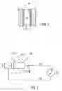
FIG. 1 shows a component with a sensor, which component is coated, with the method according to an embodiment of the invention being used for layer thickness determination, and
FIG. 2 shows a measuring arrangement having a sensor for the method according to an embodiment of the invention.
DETAILED DESCRIPTION OF THE PREFERRED EMBODIMENTSFIG. 1 shows a hollow component 1 which is to be coated, for example, on an inner surface 4. However, the method can also be used for the in situ layer thickness determination of external surfaces.
A layer 7 of the material M is applied to the inner surface 4 by means of known processes, such as for example CVD (chemical vapor deposition) processes, electrochemical processes or other known coating processes. A sensor 10 is arranged in the cavity 19 of the component 1 and is therefore coated in the same way as the component 1 which is to be treated.
FIG. 2 shows an enlarged view of the sensor 10.
The sensor 10 consists of a material which has an electrical property, such as for example its electrical resistance, impedance, capacitance or the like, which changes as a result of some form of interaction with the material M which forms the layer. The sensor 10 may be of any desired shape, i.e. may, for example, be a piece of wire or in the shape of a small plate.
The sensor 10 is connected to an electrical measuring unit 16 via electrical lines 13; the measuring unit measures the electrical parameter which changes as a result of the sensor 10 being coated with the material M. The way in which the layer thickness is dependent on the electrical variable is known from calibration curves determined in preliminary tests.
The method is used in particular for internal alitizing processes in which aluminum is applied to an inner surface 4 of a component 1 (M=Al). In this case, the sensor consists, for example, of the material MCrAlY (M=Fe, Co, Ni) and changes with the aluminum applied during a CVD process in such a manner that the measured electrical characteristic variable changes in a manner which is representative of the coating result.
LIST OF REFERENCE SYMBOLS
- 1 Component
- 4 Inner surface
- 7 Layer
- 10 Sensor
- 13 Electrical line
- 16 Electrical evaluation/control
- 19 Cavity
The invention being thus described, it will be obvious that the same may be varied in many ways. Such variations are not to be regarded as a departure from the spirit and scope of the invention, and all such modifications as would be obvious to one skilled in the art are intended to be included within the scope of the following claims.
Claims
1. A device for in situ layer thickness determination during a coating process, comprising:
a sensor, adapted to be changed by the coating process in such a way that, as a result, an electrical property of the sensor which bears a correlation to the layer thickness is influenced; and
means for measuring the change in the electrical property to determine the layer thickness.
2. The device as claimed in claim 1, wherein the sensor consists of MCrAlY, where M is an element selected from the group consisting of iron, cobalt and nickel.
3. The device as claimed in claim 1, wherein the coating process is an alitizing process.
4. The device as claimed in claim 1, wherein the electrical property is the electrical resistance.
5. The device as claimed in claim 1, wherein the sensor is a sintered part.
6. The device as claimed in claim 1, wherein the coating process is a chemical vapor deposition process.
7. The device as claimed in claim 1, wherein the coating process is used for the internal coating of a component.
Images & Drawings included:

Sources:
- United States Patent and Trademark Office - verify current appl. status at the USPTO↗
Recent applications in this class:
- » 20240263300 2024-08-08
CONTROL SYSTEM OF DEPOSITION SOURCE - » 20230304144 2023-09-28
FILM FORMATION DEVICE - » 20220341032 2022-10-27
Electronic device and manufacturing method thereof - » 20220316050 2022-10-06
PVD THICKNESS CONTROL - » 20210230741 2021-07-29
Film Forming Method - » 20200224306 2020-07-16
Method of coating substrates - » 20190242010 2019-08-08
Methods for controlling physical vapor deposition metal film adhesion to substrates and surfaces - » 20190144992 2019-05-16
SPUTTERING APPARATUS AND METHOD OF OPERATING THE SAME - » 20180274086 2018-09-27
Manufacturing method of magnetic recording medium, film formation system of multilayer film, and film formation adjustment method - » 20170152597 2017-06-01
SUBSTRATE EVAPORATION-COATING DEVICE AND EVAPORATION-COATING METHOD