Active dropout optimization for current mode LDOs
US20060033481A1
2006-02-16
11/199,326
2005-08-08
✅ Patent granted
US 7,282,895 B2
2007-10-16
-
-
Karl Easthom | Harry Behm
2025-08-08
Abstract:
A DC/DC converter has a linear voltage regulator for reducing or eliminating the output ripple of the converter with a minimum loss of efficiency. The converter comprises a converter stage with a supply voltage input, a converted voltage output and a control input, a regulator stage having an input connected to the converted voltage output of the converter stage and an output connected to a load, and a tracking circuit with inputs for a voltage at the converted voltage output of the converter stage, a voltage at the output of the regulator stage and a load sense current, and an output connected to the control input of the converter stage. The tracking circuit controls the converter stage so as to increase the converted voltage with an increasing load sense current and vice versa. The output voltage of the converter is always just sufficient to eliminate the ripple without having to operate the regulator's pass transistor in its linear range.
Inventors:
- Erich Bayer 24 🇩🇪 Thonhausen, Germany
- Gerhard Thiele 4 🇩🇪 Muenchen, Germany
- Gerhard Thiele 4 🇩🇪 Munich, Germany
Assignee:
- TEXAS INSTRUMENTS INCORPORATED 18,931 🇺🇸 Dallas, TX, United States
Interested in similar patents?
Get notified when new applications in this technology area are published.
Classification:
G05F3/262 » CPC main
Regulating voltage or current wherein the variable is dc using uncontrolled devices with non-linear characteristics being semiconductor devices using diode- transistor combinations; Current mirrors using field-effect transistors only
H02M1/0045 » CPC further
Details of apparatus for conversion Converters combining the concepts of switch-mode regulation and linear regulation, e.g. linear pre-regulator to switching converter, linear and switching converter in parallel, same converter or same transistor operating either in linear or switching mode
G05F1/56 IPC
Automatic systems in which deviations of an electric quantity from one or more predetermined values are detected at the output of the system and fed back to a device within the system to restore the detected quantity to its predetermined value or values, i.e. retroactive systems; Regulating voltage or current wherein the variable actually regulated by the final control device is dc using semiconductor devices in series with the load as final control devices
G05F1/00 IPC
Automatic systems in which deviations of an electric quantity from one or more predetermined values are detected at the output of the system and fed back to a device within the system to restore the detected quantity to its predetermined value or values, i.e. retroactive systems
G05F1/613 IPC
Automatic systems in which deviations of an electric quantity from one or more predetermined values are detected at the output of the system and fed back to a device within the system to restore the detected quantity to its predetermined value or values, i.e. retroactive systems; Regulating voltage or current wherein the variable actually regulated by the final control device is dc using semiconductor devices in parallel with the load as final control devices
Description
The present invention relates to a DC/DC converter with a linear regulator for reducing the output ripple of the converter.
BACKGROUND OF THE INVENTIONThe output voltage of a conventional DC/DC converter operating in a switched mode usually has a considerable ripple. This is especially the case for converters with hysteretic control. When such ripple cannot be tolerated for a particular application, a linear regulator is inserted between the output of the converter stage and the load to eliminate the ripple. Since the voltage regulator is not aware of the load requirements, the output voltage of the converter is adjusted to a level sufficient for the regulator to eliminate the ripple under all load conditions. As a consequence, the load current pass transistor in the voltage regulator usually operates in an unsaturated condition, resulting in a considerable loss of efficiency.
BRIEF SUMMARY OF THE INVENTIONThe present invention provides a DC/DC converter with a linear regulator for reducing or eliminating the output ripple of the converter with a minimum loss of efficiency.
In a described embodiment, the converter comprises a converter stage, a regulator stage, and a tracking circuit. The converter stage has a supply voltage input, a converted voltage output and a control input. The regulator stage has an input connected to the converted voltage output of the converter stage and an output connected to a load. The tracking circuit has inputs for a voltage at the converted voltage output of the converter stage, a voltage at the output of the regulator stage and a load sense current, and an output connected to the control input of the converter stage. The tracking circuit controls the converter stage so as to increase the converted voltage with an increasing load sense current and vice versa. Accordingly, the output voltage of the converter is always just sufficient to eliminate the ripple without having to operate the regulator's pass transistor in its linear range.
In a detailed implementation, the linear regulator includes a load current pass transistor in MOS technology and the tracking circuit controls the converter stage such that the voltage at the converted voltage output of the converter stage is just sufficient to avoid operation of the load current pass transistor in an unsaturated state. As a power MOS transistor has virtually no voltage loss in its saturated state, a loss of efficiency is avoided.
BRIEF DESCRIPTION OF THE DRAWINGSFurther details of the invention will become apparent from the following description, with reference to the accompanying drawings, wherein:
FIG. 1 is a block diagram of an embodiment of the inventive DC/DC converter; and
FIG. 2 is a circuit diagram of the converter.
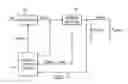
DETAILED DESCRIPTION OF EMBODIMENTSThe DC/DC converter in FIG. 1 comprises a converter stage 10, a current mode LDO (Low Dropout regulator or Linear Dropout regulator) 12 and a Dropout Tracking Circuit 14. An input voltage VIN of a system is converted (by means of a Buck-, Boost-Converter, Charge Pump, or other suitable means) to a certain output converter voltage at VBOOT (see FIG. 1). A current mode LDO converts the relative high ripple voltage at VBOOT to a low ripple voltage at VMAIN. The dropout tracking circuit compares the voltages VBOOT with VMAIN and sends a Control Signal which is dependent on the load current ILOAD to the voltage converter (e.g., to change Duty Cycle of the Voltage Converter). The goal of this configuration is a low ripple output voltage VMAIN without high efficiency losses. To minimize the efficiency losses the dropout of the Linear Dropout Regulator is regulated via the dropout tracking circuit.
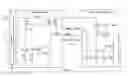
FIG. 2 shows further details of a particular implementation. In the Current Mode LDO 12, the compensated (Cc, Re) gm-stage compares the feedback voltage on the divider node between resistors R2 and R3 with a reference voltage VREF. The output of the gm-stage controls the source follower transistor M1. This follower works as a voltage to current converter. The current through resistor R1 is mirrored via transistor M2 with a current amplification k to the pass transistor M3. Dependent on the output load of the LDO, the gate-source voltage of transistor M3 is controlled. The sense transistor M4 sends an ILOAD proportional current to the Dropout Tracking Circuit 14.
The Dropout Tracking Circuit 14 includes a hysteretic comparator, specifically, the hysteretic comparator compares the voltage VMAIN with voltage VX=VBOOT−dV. The offset voltage dV is proportional to the dropout of the LDO pass element transistor M3. Voltage Vx depends on the load current. For higher load current, dV increases and the comparator sends a Control Signal to the converter to increase the voltage VBOOT. This also means an increase in dropout voltage (VDS) of transistor M3.
The Converter 10 is controlled by an output of the Dropout Tracking Circuit 14. The ILOAD dependent control signal of the Dropout Tracking Circuit controls the converter output voltage VBOOT, e.g., by changing the duty cycle. Depending on the type of “Dropout Tracking Circuit” (hysteretic with comparator or linear with OP-AMP), the converter could run as a hysteretic or linear regulated PWM converter (e.g. Buck- or Boost Converter). Advantages of the present invention are: With Current Mode LDO extremely low output voltage ripple (compared with a converter only); minimized LDO dropout to guarantee power supply rejection and optimized efficiency; possible for all Converter Topologies: Buck-, Boost-Converter, Charge Pumps; and the converter can be regulated in a PFM mode without sacrificing ripple performance.
Claims
1. A DC/DC converter with a linear regulator for reducing the output ripple of the converter, comprising:
a converter stage having a supply voltage input, a converted voltage output and a control input;
a regulator stage having an input connected to the converted voltage output of the converter stage and an output connected to a load, and
a tracking circuit with input for a voltage at the converted voltage output of the converter stage, input for a voltage at the output of the regulator stage and a load sense current, and an output connected to the control input of the converter stage;
wherein the tracking circuit controls the converter stage so as to increase the converted voltage with an increasing load sense current, and vice versa.
2. The DC/DC converter of claim 1, wherein the linear regulator includes a load current pass transistor in MOS technology, and the tracking circuit controls the converter stage such that the voltage at the converted voltage output of the converter stage is sufficient to avoid operation of the load current pass transistor in an unsaturated state.
3. The DC/DC converter of claim 2, wherein the linear regulator includes a feedback loop with a comparator that compares a feedback voltage derived from the output of the regulator with a reference voltage and an output that controls the pass transistor.
4. The DC/DC converter according to claim 3, wherein the linear regulator includes a current mirror associated with the pass transistor and providing the load sense current.
5. The DC/DC converter according to claim 2, wherein the linear regulator includes a current mirror associated with the pass transistor and providing the load sense current.
Images & Drawings included:

Sources:
- United States Patent and Trademark Office - verify current appl. status at the USPTO↗
Recent applications in this class:
- » 20250291377 2025-09-18
CIRCUIT AND SYSTEM FOR ACTIVELY DISCHARGING A POWER STAGE INPUT NODE DURING POWER SUPPLY TURN-ON - » 20250284306 2025-09-11
Bias Circuit and the Control Method thereof - » 20250284305 2025-09-11
VOLTAGE REFERENCE CIRCUIT USING FIELD-EFFECT TRANSISTORS - » 20250271889 2025-08-28
Leakage Insensitive Switch Control for Bandgap Thermal Sensors in Core-MOS Nodes - » 20250264901 2025-08-21
FAST POWER-UP SCHEME FOR CURRENT MIRRORS - » 20250264900 2025-08-21
LOW VOLTAGE CASCODE CURRENT MIRROR - » 20250264899 2025-08-21
BIASING CIRCUIT - » 20250251749 2025-08-07
Controllable Temperature Coefficient Bias Circuit - » 20250224752 2025-07-10
Bandgap Circuit Having A Base Current Redistribution Circuit - » 20250216884 2025-07-03
REFERENCE CURRENT GENERATING CIRCUIT AND ASSOCIATED CALIBRATION METHOD
Recent applications for this Assignee:
- » 20250291595 2025-09-18
CIRCUIT, SYSTEM, AND METHOD FOR MATRIX DECIMATION - » 20250286550 2025-09-11
TRANSISTOR SHUTDOWN CIRCUT - » 20250279725 2025-09-04
CONDUCTION MODE CONTROL - » 20250274138 2025-08-28
SWITCH REGULATOR - » 20250267687 2025-08-21
ENHANCED BROADCAST TRANSMISSION IN UNSLOTTED CHANNEL HOPPING MEDIUM ACCESS CONTROL - » 20250266825 2025-08-21
BOOTSTRAP CIRCUIT - » 20250247097 2025-07-31
LEVEL SHIFTER CIRCUIT - » 20250247082 2025-07-31
LOW AREA AND POWER MULTI-BIT FLIP-FLOP - » 20250246995 2025-07-31
SWITCHING CONVERTER DEADTIME CONTROL - » 20250246345 2025-07-31
TRIMMING RESISTOR USING MODULATED SIGNAL