Use of an organic matrix material for producing an organic semiconductor material, organic semiconductor material and electronic component
US20060049397A1
2006-03-09
11/196,491
2005-08-03
✅ Patent granted
US 7,540,978 B2
2009-06-02
-
-
Mark Kopec | Jaison P Thomas
2025-12-29
Abstract:
The present invention relates to use of an organic matrix material for producing an organic semiconductor material, characterized in that the organic matrix material is comprised at least partly of a spirobifluorene compound, and the glass transition temperature of the organic matrix material is at least 120° C. and the highest occupied molecular orbital (HOMO) of the matrix material is at a maximum energy level of 5.4 eV; and also to an organic semiconductor material and electronic component.
Inventors:
- Martin Pfeiffer 31 🇩🇪 Dresden, Germany
- Jan Blochwitz-Nimoth 17 🇩🇪 Dresden, Germany
- Andrea Lux 20 🇩🇪 Dresden, Germany
- Josef Salbeck 1 🇩🇪 Kassel, Germany
Assignee:
- NOVALED AG 84 🇩🇪 Dresden, Germany
Interested in similar patents?
Get notified when new applications in this technology area are published.
Classification:
H05B33/14 » CPC main
Electroluminescent light sources; Light sources with substantially two-dimensional radiating surfaces characterised by the chemical or physical composition or the arrangement of the electroluminescent material, or by the simultaneous addition of the electroluminescent material in or onto the light source
C09K11/06 » CPC further
Luminescent, e.g. electroluminescent, chemiluminescent materials containing organic luminescent materials
H01L51/006 » CPC further
Solid state devices using organic materials as the active part, or using a combination of organic materials with other materials as the active part; Processes or apparatus specially adapted for the manufacture or treatment of such devices, or of parts thereof; Selection of organic semiconducting materials, e.g. organic light sensitive or organic light emitting materials; Macromolecular systems with low molecular weight, e.g. cyanine dyes, coumarine dyes, tetrathiafulvalene; Amine compounds having at least two aryl rest on at least one amine-nitrogen atom, e.g. triphenylamine comprising polycyclic condensed aromatic hydrocarbons as substituents on the nitrogen atom
C09K2211/1007 » CPC further
Chemical nature of organic luminescent or tenebrescent compounds; Non-macromolecular compounds; Carbocyclic compounds Non-condensed systems
C09K2211/1011 » CPC further
Chemical nature of organic luminescent or tenebrescent compounds; Non-macromolecular compounds; Carbocyclic compounds Condensed systems
C09K2211/1014 » CPC further
Chemical nature of organic luminescent or tenebrescent compounds; Non-macromolecular compounds; Carbocyclic compounds bridged by heteroatoms, e.g. N, P, Si or B
H01L51/5048 » CPC further
Solid state devices using organic materials as the active part, or using a combination of organic materials with other materials as the active part; Processes or apparatus specially adapted for the manufacture or treatment of such devices, or of parts thereof specially adapted for light emission, e.g. organic light emitting diodes [OLED] or polymer light emitting devices [PLED] Carrier transporting layer
Y02E10/549 » CPC further
Energy generation through renewable energy sources; Photovoltaic [PV] energy Organic PV cells
Y02E10/549 » CPC further
Energy generation through renewable energy sources; Photovoltaic [PV] energy Organic PV cells
H01B1/12 IPC
Conductors or conductive bodies characterised by the conductive materials; Selection of materials as conductors mainly consisting of other non-metallic substances organic substances
C07C211/54 IPC
Compounds containing amino groups bound to a carbon skeleton having amino groups bound to carbon atoms of six-membered aromatic rings of the carbon skeleton having amino groups bound to two or three six-membered aromatic rings
H01B1/00 IPC
Conductors or conductive bodies characterised by the conductive materials; Selection of materials as conductors
H01L29/08 IPC
Semiconductor devices adapted for rectifying, amplifying, oscillating or switching, or capacitors or resistors with at least one potential-jump barrier or surface barrier, e.g. PN junction depletion layer or carrier concentration layer; Details of semiconductor bodies or of electrodes thereof; Multistep manufacturing processes therefor; Semiconductor bodies ; Multistep manufacturing processes therefor characterised by their shape; characterised by the shapes, relative sizes, or dispositions of the semiconductor regions ; characterised by the concentration or distribution of impurities within semiconductor regions with semiconductor regions connected to an electrode carrying current to be rectified, amplified or switched and such electrode being part of a semiconductor device which comprises three or more electrodes
H01J1/62 IPC
Details of electrodes, of magnetic control means, of screens, or of the mounting or spacing thereof, common to two or more basic types of discharge tubes or lamps; Screens on or from which an image or pattern is formed, picked-up, converted, or stored; Luminescent coatings on vessels Luminescent screens; Selection of materials for luminescent coatings on vessels
H01L31/00 IPC
Semiconductor devices sensitive to infra-red radiation, light, electromagnetic radiation of shorter wavelength or corpuscular radiation and specially adapted either for the conversion of the energy of such radiation into electrical energy or for the control of electrical energy by such radiation; Processes or apparatus specially adapted for the manufacture or treatment thereof or of parts thereof; Details thereof
Description
TECHNICAL FIELDThe present invention relates to the use of an organic matrix material for producing an organic semiconductor material, and also to an organic semiconductor material comprising an organic matrix material and an organic dopant, and also to an electronic component.
BACKGROUND OF THE INVENTIONIt is known that doping can alter organic semiconductors with regard to their electrical properties, in particular their electrical conductivity, as is also the case for inorganic semiconductors such as silicon semiconductors.
In this case, generation of charge carriers in a matrix material increases the initially quite low conductivity and, depending on the type of the dopant used, achieves a change in the Fermi level of the semiconductor. Doping leads to an increase in the conductivity of the charge transport layer, which reduces resistance losses, and leads to an improved transition of the charge carriers between contacts and organic layer.
For the doping of such organic semiconductors, strong electron acceptors such as tetracyanoquinonedimethane (TCNQ) or 2,3,5,6-tetrafluorotetracyano-1,4-benzoquinone-dimethane (F4-TCNQ) have become known; see M. Pfeiffer, A. Beyer, T. Fritz, K. Leo, Appl. Phys. Lett., 73 (22), 3202-3204 (1998) and J. Blochwitz, M. Pfeiffer, T. Fritz, K. Leo, Appl. Phys. Lett., 73 (6), 729-732 (1998). As a result of electron transfer processes in electron donor-like base materials (hole transport materials), these generate what are known as holes, the number and mobility of which more or less significantly alter the conductivity of the matrix material.
Known matrix materials are, for example, starburst compounds such as 4,4′,4″-tris(diphenylamino)triphenylamine (TDATA), 4,4′,4″-tris(3-methylphenylphenylamino)-triphenylamine (m-MTDATA) and N,N,N′,N′-tetrakis(4-methoxyphenyl)benzidine (MeO-TPD).
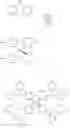
The chemical structure of the abovementioned known matrix materials is shown below.
| m-MTDATA |
| TDATA |
| MeO-TPD |
However, these compounds are thermally unstable, i.e. they have a low glass transition temperature and tend to crystallization at low temperatures, which leads ultimately to unstable electronic components.
The glass transition temperature is regarded as being the temperature at which motion of the molecules in the event of rapid cooling of the material from the melt is no longer possible for kinetic reasons, and thermodynamic parameters such as the heat capacity or the coefficient of expansion suddenly change from typical liquid values to typical solid values. The thermal stability of the matrix material is of significance especially for morphological reasons when organic semiconductor materials are used with such matrix materials, in order to prevent the formation of roughness at elevated operating temperatures in the customary layer structure of such semiconductor materials. Furthermore, the thermal stability is of significance, in order to restrict the diffusion of the dopant within the matrix material.
The prior art also discloses thermally stable matrix materials such as 2,2′,7,7′-tetrakis(N,N-diphenylamino)-9,9′-spirobifluorene (spiro-TAD) which, however, owing to the position of the energy level of their highest occupied molecular orbitals (HOMOs), cannot be doped.
SUMMARY OF THE INVENTIONIt is an object of the invention to provide for use of an organic matrix material for producing an organic semiconductor material, the matrix material being thermally stable and dopable, in order to provide hole transport layers having high hole conductivity for use in organic semiconductor components. Furthermore, it should be possible to apply the organic matrix materials by vapour deposition in order to provide layers having a correspondingly high hole conductivity by coevaporation under reduced pressure with a strong organic electron acceptor.
This object is achieved by the organic matrix material being comprised at least partly of a spirobifluorene compound of the formula (I)
where R is at least one substituent on a phenyl radical, but not all of R are simultaneously hydrogens,
and/or of the formula (II)
where R is a substituent apart from hydrogen and R′ is a substituent,
the glass transition temperature of the organic matrix material being at least 120° C. and the highest occupied molecular orbital (HOMO) of the matrix material lying at a maximum energy level of 5.4 eV. In formula (I), a phenyl radical may thus be provided with one or more substituents.
It is preferred that each R and/or R′ in formula (I) and (II) is independently selected from the group consisting of hydrogen, methyl, ethyl, n-propyl, isopropyl, n-butyl, isobutyl, tert-butyl, NH2, N(CH4)2 and NPh2, where not all R in formula (I) are simultaneously hydrogens.
It is particularly preferred that the spirobifluorene compound is selected from the group consisting of
It is likewise preferred that the glass transition temperature of the spirobifluorene compound lies between 120° C. and 250° C., and the highest occupied molecular orbital of the compound lies at an energy level between 4.5 eV and 5.4 eV, preferably between 4.8 eV and 5.2 eV.
The object is also achieved by an organic semiconductor material comprising an organic matrix material and an organic dopant, the organic matrix material at least partly comprising one or more compounds which are used as matrix materials in accordance with the invention.
It is likewise preferred that the dopant is 2,3,5,6-tetrafluoro-7,7,8,8-tetracyanoquinodimethane or a derivative thereof. However, further dopants having similar acceptor action and equal or larger molecular mass are possible; see, for example, DE10357044.6. It is particularly preferred that the molar doping ratio of dopant to matrix material is between 1:1 and 1:10 000.
The object is further achieved by an electronic component in which an organic matrix material is used which is comprised at least partly of a spirobifluorene compound which is envisaged as a matrix material in accordance with the invention.
Finally provided is the electronic component in the form of an organic light-emitting diode (OLED), a photovoltaic cell, an organic solar cell, an organic diode or an organic field-effect transistor.
The invention is based on the surprising finding that use of the organic matrix material described for producing an organic semiconductor material affords thermally stable and doped hole transport layers for use in organic semiconductor components. The use of the matrix materials provides bole transport materials which can be applied by vapour deposition, so that they lead, by coevaporation under reduced pressure with a strong organic electronic acceptor, to layers having a high hole conductivity.
When the organic matrix materials described are used, a stable, singly positively charged cationic state of the hole transport material is achieved.
Further advantages and features of the present invention are evident from the detailed description of exemplary organic matrix materials which follows, and also the appended drawings, in which
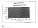
BRIEF DESCRIPTION OF DRAWINGSFIG. 1 shows the dependence of the lateral current on the layer thickness for a transport layer of the organic matrix material spiro-TTB (doped with F4-TCNQ);
FIG. 2 shows the dependence of the lateral current on the layer thickness for a transport layer of the organic matrix material spiro-iPr-TAD (doped with F4-TCNQ); and
FIG. 3 shows the luminance voltage and power efficiency voltage characteristics of an organic light-emitting diode having doped transport layers and spiro-TFB (doped with F4 TCNQ) as a p-dopant.
DETAILED DESCRIPTION OF EMBODIMENTS EXAMPLES A. Preparation of 2,2′,7,7′-tetrakis(N,N-di-p-methylphenylamino)-9,9′-spirobifluorene (spiro-TTB)
2,2′,7,7′-Tetrabromo-9,9′-spirobifluorene (10 g, 15.8 mmol), di-p-tolylamine (14.2 g, 72.1 mmol) and sodium tert-butoxide (9.6 g, 100 mmol) are stirred in 100 ml of anhydrous toluene under nitrogen at 60° C. for 1 h. Subsequently, tri-tert-butylphosphine. (200 mg, 1.0 mmol, 6.3% based on tetrabromospitobifluorene) and palladium(II) acetate (92 mg, 0.4 mmol, 2.6% based on tetrabromospirobifluorene) are added and the reaction mixture is heated to reflux under nitrogen. The progress of the reaction is monitored by thin-layer chromatography (eluent: 50% hexane in dicchloromethane). After 2.5 h, no reactant can any longer be detected in the TLC. The reaction mixture is cooled, admixed with a solution of 100 mg of KCN in 20 ml of water and stirred at 60° C. for another 1 h. After cooling to room temperature, the phases are separated, and the organic phase is dried over sodium sulphate and the solvent is removed. The crude product is recrystallized twice from dioxane and subsequently reprecipitated from a little dichloromethane in hexane and dried under reduced pressure.
Yield: 15.0 g (13.8 mmol, 87% of theory) of slightly greenish powder.
1H NMR (500 MHz, CDCl3+hydrazine hydrate): 7.40 (d, 1H, J=7.8), 7.00 (d, 4H, J=8.3), 6.88 (d, 4H, J=8.3), 6.85 (dd, 1H, J=8.3, J=2.0), 6.67 (d, 1H, J=2.0), 2.30 (s, 6H).
13C NMR (127.5 MHz, CDCl3+hydrazine hydrate): 149.8, 146.7, 145.3, 136.1, 131.5, 129.5, 124.0, 123.2, 119.9, 119.3, 65.3, 20.6.
B. Preparation of 2,2′,7,7′-tetrakis(N,N-di-pisupropylphenylamino)-9,9′-spirofluorene (spiro-iPr-TAD) 4-Isopropyliodobenzene
4-Isopropylaniline (49.5 g, 366 mmol) is suspended in 200 ml of dist. water and admixed gradually under ice cooling with 200 ml of semiconcentrated sulphuric acid. Subsequently, a solution of sodium nitrite (25.5 g, 370 mmol) in 200 ml dist. water is added dropwise at such a rate that the temperature does not rise above 20° C. On completion of the dropwise addition, the mixture is stirred at 2° C. for another 20 min. The resulting clear reddish diazonium salt solution is now added through a filter to a solution of potassium iodide (135.0 g, 813 mmol) in 200 ml of dist. water. The reaction mixture is stirred at 80° C. for 1 h. In the course of this, the solution becomes black with vigorous gas evolution and an oily organic phase separates out. After cooling, the organic phase is removed and the aqueous phase is extracted four times more with 100 ml of ether. The combined organic phases are washed with dilute sodium hydroxide solution and dist. water, and dried over sodium sulphate. After the solvent has been removed, the crude product is distilled in a membrane-pump vacuum. The slightly reddish target product distils over at a temperature of 100-105° C. (15 mbar).
Yield; 75.3 g (310 mmol, 83% of theory) of slightly reddish liquid.
1H NMR (500 MHz, CDCl3): 7.60 (d, 2H, J=8.3), 6.98 (d, 2H, J=8.3), 2.85 (q, 1H, J=6.8, 1.22 (d, 6H, J=6.8).
13C NMR (127.5 MHz, CDCl3): 148.4, 137.3, 128.6, 90.6, 33.7, 23.8.
N-Acetyl-4-isopropylaniline
Acetic anhydride (26.0 g, 254 mmol) is slowly added dropwise to a solution of 4-isopropylaniline (17.2 g, 127 mmol) in 80 ml of chloroform. In the course of this, intense heating of the reaction mixture occurs. On completion of the dropwise addition, the mixture is stirred at room temperature for another 2 h. The reaction mixture is concentrated to dryness and the resulting, reddish-white solid is recrystallized from hexane.
Yield: 21.1 g (120 mmol, 94% of theory) of white solid.
1H NMR (500 MHz, CDCl3): 7.88 (s, 1H), 7.40 (d, 2H, J=8.3), 7.14 (d, 2H, J=8.3), 2.86 (q, 1H, J=6.8), 1.21 (d, 6H, J=6.8).
13C NMR (127.5 MHz, CDCl3): 168.6, 144.9, 135.6, 126.7, 120.2, 33.5, 24.3, 23.9.
Melting point: 107° C. (literature (Dyall, Aus. J. Chem. 17, 1964, 419): 104-105° C.).
N-Acetyl-N,N-di(4-isopropylphenyl)amine
4-Isopropyliodobenzene (29.2 g, 118 mmol), N-acetyl-4-isopropylaniline (21.0 g, 118 mmol), copper powder (15.0 g, 237 mmol), potassium carbonate (65.4 g, 474 mmol) and 18-crown-6 (2.9 g, 12 mmol) are heated to reflux in 200 ml of 1,2-dichlorobenzene. The reaction is monitored by thin-layer chromatography (eluent: 10% THF in dichloromethane). After 48 h, the still-hot reaction mixture is filtered, the filter residue is washed thoroughly and the solvent is removed on a rotary evaporator. The crude product is chromatographed on silica gel using 10% THF in dichloromethane. The product fractions are concentrated to dryness, recrystallized from hexane and dried under reduced pressure.
Yield: 14.31 g (48 mmol, 41% of theory) of slightly brovish solid.
1H NMR (500 MHz, CDCl3): 7.21 (m, 8H), 2.90 (s (br.), 2H), 2.04 (s, 3H), 1.23 (s(br.), 12H).
N,N-Di-(4-isopropylphenyl)amine
N-Acetyl-N,N-di(4-isopropylphenyl)amine (5.4 g, 18.4 mmol) are heated to reflux in 100 ml of 20% aqueous ethanol. The reaction is monitored by thin-layer chromatography. After 30 h, no reactant is any longer detectable in the TLC. The ethanolic solution is poured into dist. water, and the brownish precipitate is filtered off with suction, dissolved in dichloromethane and dried with sodium sulphate. The solution is concentrated and chromatographed through a short silica gel column with 50% dichloromethane in hexane. The product fractions are concentrated to dryness and the product is dried under reduced pressure.
Yield: 4.0 g (16 mmol, 86% of theory) of slightly brownish solid.
1H NMR (500 MHz, CDCl3): 7.12 (d, 4H, J=8.3), 6.99 (d, 4H, J=8.3), 5.55 (s(br.), 1H), 2.86 (q, 2H, J=6.8), 1.24 (d, 12H, J=6.8).
13C NMR (127.5 MHz, CDCl3): 141.3, 127.1, 117.7, 33.4, 24.1.
2,2′,7,7′-Tetrakis(N,N-di-p-isopropylphenylamino)-9,9′-spirobifluorene (spiro-iPr-TAD)
2,2′,7,7′-Tetrabromo-9,9′-spirobifluorene (1.7 g, 2.6 mmol), N,N-di-4-isopropylphenylamine (3.0 g, 12.0 mmol) and sodium tert-butoxide (1.6 g, 17 mmol) are stirred in 100 ml of anhydrous toluene under nitrogen at 60° C. for 1 h. Subsequently, tri-tert-butylphosphine (4.8 mg, 0.24 mmol, 9.2% based on tetrabromospirobifluorene) and palladium(II) acetate (27 mg, 0.12 mmol, 4.6% based on tetrabromospirobifluoreie) are added and the reaction mixture is heated to reflux under nitrogen. The progress of the reaction is monitored by thin-layer chromatography (eluent: 20% dichloromtethane in hexane). After 3.5 h, no reactants can any longer be detected in the TLC. The reaction mixture is cooled, admixed with a solution of 100 mg of KCN in 20 ml of water, and stirred at 60° C. for another 1 h. After cooling to room temperature, the phases are separated, and the organic phase is dried over sodium sulphate and the solvent is removed. The crude product is recrystallized twice from dioxane and subsequently dried under reduced pressure.
Yield: 2.8 g (2.1 mmol, 81% of theory) of slightly yellowish, finely crystalline powder.
1H NMR (500 MHz, CDCl3): 7.41 (d, 1H, J=8.3), 7.05 (d, 4H, J=8.3), 6.90 (m, 5H). 6.72 (s (br.) 1H), 2.85 (q, 2H, J=6.8), 1.24 (d, 12H, J=6.8).
13C NMR (127.5 MHz, CDCl3): 150.7, 147.5, 146.3, 143.3, 137.2, 127.6, 125.3, 123.8, 120.8, 120.7, 66.2, 34.1, 24.8.
Tg: 144° C., Tk: 166° C., Tm: 363° C.
The two organic materials spiro-TTB and spiro-iPr-TAD were each doped with F4-TCNQ and tested in conductivity measurements. For these measurements, the doped layer was applied by coevaporation under reduced pressure over two approx. 5 mm-wide contacts (made of indium tin oxide, ITO) which, were applied to a glass substrate at a distance of 1 mm from one another. The contacts were connected externally to a current-voltage measuring instrument, which allowed the lateral current to be measured at a fixed applied voltage. From this lateral current, the conductivity of the layer is then calculated by a simple resistance relationship. The conductivity can be determined with the aid of the following equation:
Conductivity=(lateral current*distance)/(width*layer thickness)
FIGS. 1 and 2 each show the increase in the lateral current with the layer thickness for the two doped matrix materials. The conductivity of a 50 nm-thick layer of spiro-TTB doped with 2.5% F4-TCNQ is approx. 1.6 E-5 S/cm, while the conductivity of a 50 nm-thick layer of spiro-iPr-TAD doped with 5% F4-TCNQ is approx. 8 E-7 S/cm.
One embodiment of an inventive electronic component in the form of an OLED with an organic matrix material, as is to be used in accordance with the invention, can be produced and comprises, in the case of normal design emitting through the substrate, the following layer arrangement:
-
- 1. carrier substrate: glass,
- 2. bottom electrode (anode A): ITO,
- 3. p-doped, hole-injecting and -transporting layer: spiro-TTB: F4TCNQ (2.5% molar doping concentration),
- 4. thin bole-side intermediate layer of a material whose band positions match the band positions of the layers surrounding them: spiro-TAD,
- 5. light-emitting layer (possibly doped with emitter dye): TCTA (4,4′,4″-tris(N-carbazolyl)triphenylamine): Irppy 3 (fac-tris(2-phenylpyridine)iridium),
- 6. thin electron-side intermediate layer of a material whose band positions match the band positions of the layers surrounding them: BPhen (4,7-diphenyl-1,10-phenanthroline),
- 7. n-doped, electron-injecting and -transporting layer BPhen doped with caesium (approx. 1:1 molar concentration),
- 8. top electrode (cathode K): aluminum, and
- 9. encapsulation for exclusion of environmental influences: covering glass
A thus produced organic light-emitting diode was examined with regard to the luminance voltage and current efficiency voltage characteristics, the results of which are shown in FIG. 3. Due to the doping of the organic hole transport layer, his exhibits a very steep current-voltage characteristics and thus a very steep luminance voltage characteristics (left-hand axis). The luminance of 100 cd/m2 and 1000 cd/m2 are attained at voltages of 2.75 V and 3.1 V. Owing to the ideal arrangement of the doped hole and electron transport layers and of the two intermediate layers, the current efficiencies of light generation are likewise very high and constant over a wide brightness range: 46 cd/A and 45 cd/A. Owing to the stable hole transport layer, this OLED can be operated stably at relatively high temperatures (up to above 100° C.) without a reduction in the optoelectronic properties.
Features of the invention disclosed in the above description, in the claims and in the drawings may be essential either individually or in any combination for the realization of the invention in its different embodiments.
Claims
1. Use of an organic matrix material for producing an organic semiconductor material, characterized in that the organic matrix material is comprised at least partly of a spirobifluorene compound of the formula (I)
where R is at least one substituent on a phenyl radical, but not all of R are simultaneously hydrogens, and/or of the formula (II)
where R is a substituent apart from hydrogen and R′ is a substituent,
the glass transition temperature of the organic matrix material being at least 120° C. and the highest occupied molecular orbital (HOMO) of the matrix material lying at a maximum energy level of 5.4 eV.
2. Use of an organic matrix material according to claim 1, characterized in that each R and/or R′ in formula (I) and formula (II) is independently selected from the group consisting of hydrogen, methyl, ethyl, n-propyl, isopropyl, n-butyl, isobutyl, tert-butyl, NH2, N(CH4)2 and NPh2, where not all R in formula (I) are simultaneously hydrogens.
3. Use of an organic matrix material according to claim 2, characterized in that the spirobifluorene compound is selected from the group consisting of
4. Use of an organic matrix material according to claim 1, characterized in that the glass transition temperature of the spirobifluorene compound lies between 120° C. and 250° C., and the highest occupied molecular orbital of the compound lies at an energy level between 4.5 eV and 5.4 eV, preferably between 4.8 eV and 5.2 eV.
5. Organic semiconductor material comprising an organic matrix material and an organic dopant, characterized in that the organic matrix material at least partly comprises one or more compounds selected from the group consisting of a spirobifluorene compound of the formula (I)
where R is at least one substituent on a phenyl radical, but not all of R are simultaneously hydrogens, and/or of the formula (II)
where R is a substituent apart from hydrogen and R′ is a substituent,
the glass transition temperature of the organic matrix material being at least 120° C. and the highest occupied molecular orbital (HOMO) of the matrix material lying at a maximum energy level of 5.4 eV.
6. Organic semiconductor material according to claim 5, characterized in that the dopant is 2,3,5,6-tetrafluoro-7,7,8,8-tetracyanoquinodimethane or a derivative thereof.
7. Organic semiconductor material according to claim 5, characterized in that the molar doping ratio of dopant to matrix material is between 1:1 and 1:10.000.
8. Electronic component including an organic semiconductor material comprising an organic matrix material and an organic dopant, characterized in that the organic matrix material is comprised at least partly of a spirobifluorene compound selected from the group consisting of a spirobifluorene compound of the formula (I)
where R is at least one substituent on a phenyl radical, but not all of R are simultaneously hydrogens, and/or of the formula (II)
where R is a substituent apart from hydrogen and R′ is a substituent,
the glass transition temperature of the organic matrix material being at least 120° C. and the highest occupied molecular orbital (HOMO) of the matrix material lying at a maximum energy level of 5.4 eV.
9. Electronic component according to claim 8 in the form of an organic light-emitting diode (OLED), a photovoltaic cell, an organic solar cell, an organic diode or an organic field-effect transistor.
10. Organic semiconductor material according to claim 5, characterized in that each R and/or R′ in formula (I) and formula (II) is independently selected from the group consisting of hydrogen, methyl, ethyl, n-propyl, isopropyl, n-butyl, isobutyl, tert-butyl, NH2, N(CH4)2 and NPh2, where not all R in formula (I) are simultaneously hydrogens.
11. Organic semiconductor material according to claim 10, characterized in that the spirobifluorene compound is selected from the group consisting of
12. Organic semiconductor material according to claim 5, characterized in that the glass transition temperature of the spirobifluorene compound lies between 120° C. and 250° C., and the highest occupied molecular orbital of the compound lies at an energy level between 4.5 eV and 5.4 eV, preferably between 4.8 eV and 5.2 eV.
13. Electronic component according to claim 8, characterized in that each R and/or R′ in formula (I) and formula (II) is independently selected from the group consisting of hydrogen, methyl, ethyl, n-propyl, isopropyl, n-butyl, isobutyl, tert-butyl, NH2, N(CH4)2 and NPh2, where not all R in formula (I) are simultaneously hydrogens.
14. Electronic component according to claim 13, characterized in that the spirobifluorene compound is selected from the group consisting of
15. Electronic component according to claim 8, characterized in that the glass transition temperature of the spirobifluorene compound lies between 120° C. and 250° C., and the highest occupied molecular orbital of the compound lies at an energy level between 4.5 eV and 5.4 eV, preferably between 4.8 eV and 5.2 eV.
Images & Drawings included:


Sources:
- United States Patent and Trademark Office - verify current appl. status at the USPTO↗
Recent applications in this class:
- » 20250247927 2025-07-31
ELECTRONIC DEVICE - » 20250193977 2025-06-12
COMPOSITE LIGHT EMISSION SIGNAL GENERATION MATERIAL FOR STATE SENSING, LIGHT-EMITTING SUBSTANCE CARRIER, INK FOR STATE SENSING, MEASUREMENT CHIP, AND ANALYSIS METHOD - » 20240314898 2024-09-19
Functional Panel, Display Device, Input/Output Device, and Data Processing Device - » 20240268005 2024-08-08
Electronic device - » 20230397306 2023-12-07
Electroluminescent ceramic materials - » 20230276548 2023-08-31
ELECTROLUMINESCENT SYSTEM AND PROCESS - » 20230232509 2023-07-20
Display device - » 20220418059 2022-12-29
BLUE ORGANIC ELECTROLUMINESCENCE DEVICE, DISPLAY PANEL AND DISPLAY APPARATUS - » 20220338316 2022-10-20
Functional panel, display device, input/output device, and data processing device - » 20210185776 2021-06-17
Method of manufacturing display device
Recent applications for this Assignee:
- » 20140340128 2014-11-20
Organic zener diode, electronic circuit, and method for operating an organic zener diode - » 20140284567 2014-09-25
Vertical organic transistor, circuit configuration and arrangement with vertical organic transistors and method of manufacturing - » 20140203254 2014-07-24
Organic Electronic Component - » 20140174537 2014-06-26
Compound for organic electronic device - » 20140144509 2014-05-29
Compounds for Organic Photovoltaic Devices - » 20140070145 2014-03-13
Oxocarbon-, pseudooxocarbon- and radialene compounds and their use - » 20130320307 2013-12-05
Organic light emitting device - » 20130210192 2013-08-15
Semiconductor component - » 20130200341 2013-08-08
Electronic device comprising an organic semiconducting material - » 20130193871 2013-08-01
Large area light emitting device comprising organic light emitting diodes