Asynchronous BTL design for a Class-D audio amplifier
US20060125554A1
2006-06-15
11/041,237
2005-01-25
✅ Patent granted
US 7,209,003 B2
2007-04-24
-
-
Robert Pascal | Hieu Nguyen
2025-06-24
Abstract:
The present invention provides an asynchronous BTL (Bridge Tied Load) design for a Class-D audio amplifier. The Class-D audio amplifier comprises two independent signal routes, each of the two independent signal routes includes a PWM (Pulse Width Modulator), a predriver and a power MOS circuit; each of the two independent signal routes receives an input signal via the PWM thereof, and outputs signal through the power MOS circuit thereof, and then cooperatively drive a loudspeaker; no synchronous signal is inputted to each of the two PWMs, and the two power MOS circuits feed back independent signals respectively to the two PWMs. The present invention omits the synchronous design of the prior art, and let the two push-pull signals required by the BTL design being processed independently, while cooperatively drive the loudspeaker.
Assignee:
- PRINCETON TECHNOLOGY CORPORATION 16 🇹🇼 Hsin Tien, Taiwan
Interested in similar patents?
Get notified when new applications in this technology area are published.
Classification:
H03F3/217 » CPC main
Amplifiers with only discharge tubes or only semiconductor devices as amplifying elements; Power amplifiers, e.g. Class B amplifiers, Class C amplifiers with semiconductor devices only Class D power amplifiers; Switching amplifiers
H03F3/181 » CPC further
Amplifiers with only discharge tubes or only semiconductor devices as amplifying elements Low frequency amplifiers, e.g. audio preamplifiers
H03F3/2171 » CPC further
Amplifiers with only discharge tubes or only semiconductor devices as amplifying elements; Power amplifiers, e.g. Class B amplifiers, Class C amplifiers with semiconductor devices only; Class D power amplifiers; Switching amplifiers with field-effect devices
H03F3/2173 » CPC further
Amplifiers with only discharge tubes or only semiconductor devices as amplifying elements; Power amplifiers, e.g. Class B amplifiers, Class C amplifiers with semiconductor devices only; Class D power amplifiers; Switching amplifiers of the bridge type
H03F3/38 IPC
Amplifiers with only discharge tubes or only semiconductor devices as amplifying elements Dc amplifiers with modulator at input and demodulator at output; Modulators or demodulators specially adapted for use in such amplifiers
Description
FIELD OF THE INVENTIONThe present invention relates to an improvement of a Class-D audio amplifier design, and more particularly to an asynchronous BTL (Bridge Tied Load) design for a Class-D audio amplifier.
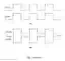
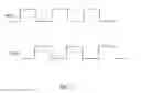
BACKGROUND OF THE INVENTIONReferring to FIGS. 1(a) and (b), which show the output carrier signals OUTA and OUTB of a push-pull type Class-D audio amplifier. The output carrier signals OUTA and OUTB of the push-pull type Class-D audio amplifier have the same carrier phase as shown in FIG. 1(a), or have a constant phase shift therebetween (for example 180°) as shown in FIG. 1(b). In general use, the output carrier signals will be filtered by a filter or human ears, therefore the synchronous design for the output carrier signals is not necessary.
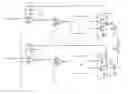
Referring to FIG. 2, which shows schematically a circuit for Class-D audio amplifier. An audio signal Vin is inputted from left to the two input terminals “a”, “b” of an operational amplifier 1. The operational amplifier 1 outputs two audio signals respectively to operational amplifier 2 and 3 (both are comparators), and then pass through the predriver 4 and 5 for driving power CMOS circuits 6 and 7 to generate output signals OUTA and OUTB. Output signals OUTA and OUTB drive the loudspeaker 8 cooperatively, this is a push-pull type circuit, and is what so-called BTL (Bridge Tied Load) design. Resistors 9 and 10 are used for feedbacking signals; capacitors 11 and 12 are compensation circuits; inductors 13, 14 and capacitors 15, 16 are filter circuits. Triangular wave Vtriangular of 500 KHz is inputted to operational amplifiers 2 and 3 for synchronizing the two carrier signals inputted to the operational amplifiers 2 and 3, therefore the phases of the carriers of output signals OUTA and OUTB will be the same with each other, as shown in FIG. 1(a); or the phases of the carriers of output signals OUTA and OUTB will have a phase shift of 180°, as shown in FIG. 1(b). The operational amplifiers 1, 2 and 3 cooperatively form a PWM (Pulse Width Modulator) for the Class-D audio amplifier. A PWM has varieties of design. FIG. 2 shows only one of them.
An additional triangular wave generator is required for generating the triangular wave Vtriangular, but a triangular wave generator is very complicated in design and is not very easy to generate very accurate triangular wave. An additional triangular wave generator will occupy too much space in an IC design, thus increasing cost. The triangular wave Vtriangular for synchronizing the two carrier signals of the output signals OUTA and OUTB is not really necessary.
Moreover, feedback signals of the output signals OUTA and OUTB via resistors 9, 10 to the operational amplifier 1 must be very accurate, otherwise the operational amplifiers 1 cannot keep its two output audio signals in balance, but this requirement causes a narrow tolerance in IC layout, thus increasing manufacturing cost.
SUMMARY OF THE INVENTIONIt is therefore an object of the invention to provide an asynchronous BTL design for a Class-D audio amplifier. Two independent signal routes are designed as shown in FIG. 3, each comprises a PWM (Pulse Width Modulator), a predriver and a power MOS circuit; each of the two independent signal routes receives an input signal via the PWM thereof, and outputs signal through the power MOS circuit thereof, and then cooperatively drive a loudspeaker; no synchronous signal is inputted to each of the two PWMs, and the two power MOS circuits feed back independent signals (before filter/after filter) respectively to the two PWMs. The present invention omits the synchronous design of the prior art, and let the two push-pull signals required by the BTL design being processed independently, while cooperatively drive the loudspeaker.
BRIEF DESCRIPTION OF THE DRAWINGSFIG. 1 shows schematically the output signals of a conventional Class-D audio amplifier.
FIG. 2 shows schematically the circuit of a conventional Class-D audio amplifier.
FIG. 3 shows schematically the circuit of a Class-D audio amplifier according to the present invention.
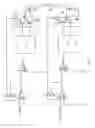
FIG. 4 shows schematically the output signals of the Class-D audio amplifier according to the present invention.
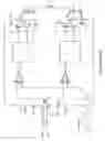
DETAILED DESCRIPTION OF THE EMBODIMENTReferring to FIG. 3, which shows an improvement for a Class-D audio amplifier according to the present invention. Audio signals Vin are inputted from left to the two input terminals “a” and “b” of operational amplifiers 21 and 22 respectively. The operational amplifiers 21 and 22 output audio signal respectively to operational amplifiers 23 and 24, and then pass through the predrivers 25 and 26 for driving power CMOS circuits 27 and 28 to generate output signals OUTC and OUTD. Output signals OUTC and OUTD cooperatively drive the loudspeaker 29. This is a push-pull type circuit, and is what so-called BTL (Bridge Tied Load) design. Resistors 30 and 31 are used for feedbacking signals; capacitors 32 and 33 are compensation circuits; inductors 34, 35 and capacitors 36, 37 are filter circuits. Each of the operational amplifiers 21, 23 and the operational amplifiers 22, 24 forms a PWM (Pulse Width Modulator) for the Class-D audio amplifier. A PWM has varieties of design. FIG. 3 shows only one of them.
The most important feature in FIG. 3 is that there is no triangular wave Vtriangular of 500 Khz inputted to the operational amplifiers 23, 24 for synchronization, therefore the output signals OUTC and OUTD have different phases, as shown in FIG. 4. This improvement omits a complicated triangular wave generator, saves the circuit space in IC layout, thereby decreasing cost. A synchronous design of triangular wave is not necessary to operational amplifiers 23 and 24, since the triangular wave just synchronizes the carrier signals. The carrier signals of the output signals OUTC and OUTD will be filtered by a filter circuit or by human ears, so the synchronization for carriers is not important.
In FIG. 2, feedback signals of the OUTA and OUTB via resistors 9, 10 to the operational amplifier 1 must be very accurate, otherwise the operational amplifiers 1 cannot keep its two output audio signals in balance, but this requirement causes a narrow tolerance in IC layout, thus increasing manufacturing cost; while in FIG. 3, feedback signals of the OUTC and OUTD are independently fed to the operational amplifier 21, 22 via resistors 30, 31 respectively, this permits a broader tolerance in IC layout, thus decreasing manufacturing cost.
In FIG. 3, feedback signals of the OUTC and OUTD are independently fed to the operational amplifier 21, 22 via resistors 30, 31 respectively, this can be modified by feedbacking signals SP+ and SP− of the loudspeaker 29 to the operational amplifier 21, 22 via resistors 30, 31 respectively.
In FIG. 3, each of the CMOS circuits 27, 28 can be replaced by a MOS circuit.
The spirit and scope of the present invention depend only upon the following Claims, and are not limited by the above embodiments.
Claims
What is claimed is:1. An asynchronous BTL (Bridge Tied Load) design for a Class-D audio amplifier, the Class-D audio amplifier comprises two independent signal routes, each of the two independent signal routes includes a PWM (Pulse Width Modulator), a predriver and a power MOS circuit; each of the two independent signal routes receives an input signal via the PWM thereof, and outputs signal through the power MOS circuit thereof, and then cooperatively drive a loudspeaker; no synchronous signal is inputted to each of the two PWMs, and the two power MOS circuits feed back independent signals respectively to the two PWMs.
2. An asynchronous BTL (Bridge Tied Load) design for a Class-D audio amplifier according to claim 1, wherein a filter circuit is connected to an output terminal of each of the two power MOS circuits; output signals of the two filters cooperatively drive the loudspeaker; two input signals of the loudspeaker are fed back to the two PWMs respectively.
3. An asynchronous BTL (Bridge Tied Load) design for a Class-D audio amplifier according to claim 1, wherein the power MOS circuit is a power CMOS circuit.
4. An asynchronous BTL (Bridge Tied Load) design for a Class-D audio amplifier according to claim 2, wherein the power MOS circuit is a power CMOS circuit.
Images & Drawings included:
Sources:
- United States Patent and Trademark Office - verify current appl. status at the USPTO↗
Recent applications in this class:
- » 20250253812 2025-08-07
LOW VOLTAGE FOR AUDIO CIRCUITS, DEVICES AND METHODS - » 20250233562 2025-07-17
CLASS-D AUDIO AMPLIFIER - » 20250202444 2025-06-19
AUTO-CALIBRATION DRIVING STRENGTH SYSTEM FOR CLASS-D AMPLIFIER - » 20250167740 2025-05-22
CLASS D AMPLIFIER CAPABLE OF ANTI-CLIPPING - » 20250141412 2025-05-01
METHODS AND APPARATUS TO MODULATE SIGNALS USING MULTI-CLASS MODULATION CIRCUITRY - » 20250119110 2025-04-10
MODULATOR INTEGRATED CIRCUIT PACKAGE - » 20250112600 2025-04-03
POWER-ON AND SHUT-DOWN POP REDUCTION IN AUDIO SYSTEMS - » 20250096750 2025-03-20
VOLTAGE-TO-TIME-TO-VOLTAGE AMPLIFIER (VTVA) USING TIME DELAY - » 20240267007 2024-08-08
CLASS D AMPLIFICATION CIRCUIT - » 20240162867 2024-05-16
CLASS-D AMPLIFIER ABLE TO REDUCE POWER NOISE
Recent applications for this Assignee:
- » 20100164930 2010-07-01
Drive circuit of display and method for calibrating brightness of display - » 20090237061 2009-09-24
DC-DC conversion device with digitally controlled comparator - » 20070168787 2007-07-19
Interface circuit for using a low voltage logic tester to test a high voltage IC - » 20060268998 2006-11-30
Integrated serial data decoder - » 20060251273 2006-11-09
Circuit for reducing pulse noise caused at switching of an analog audio processing circuit - » 20060232335 2006-10-19
Method for single-ended offset compensation of an operational amplifier - » 20060215427 2006-09-28
Circuit for reducing inrush current generated during startup of a switching power supply - » 20060158392 2006-07-20
Two-part driver circuit for organic light emitting diode - » 20060145755 2006-07-06
Square wave modulation design for a class-D audio amplifier - » 20060107074 2006-05-18
Method of using scan chains and boundary scan for power saving