Receiver for a differential phase modulated signal
US20060153577A1
2006-07-13
11/330,526
2006-01-12
✅ Patent granted
US 7,480,465 B2
2009-01-20
-
-
Kenneth N Vanderpuye | Danny W Leung
2027-07-14
Abstract:
The receiver features a first splitter which divides a differential phase modulated signal into three signal components from which at least two signal components are routed via timers. The first timer has a delay of a half period of the carrier signal and thereby serves in a conventional way for phase comparison and thus for demodulation. The second timer is adjustable and is used to compensate for the dispersion.
Assignee:
- Nokia Siemens Networks GmbH Co.& KG 282 🇩🇪 Munich, Germany
Interested in similar patents?
Get notified when new applications in this technology area are published.
Classification:
H04J14/08 IPC
Optical multiplex systems Time-division multiplex systems
H04B10/69 » CPC main
Transmission systems employing electromagnetic waves other than radio-waves, e.g. infrared, visible or ultraviolet light, or employing corpuscular radiation, e.g. quantum communication; Receivers; Non-coherent receivers, e.g. using direct detection Electrical arrangements in the receiver
H04B10/677 » CPC further
Transmission systems employing electromagnetic waves other than radio-waves, e.g. infrared, visible or ultraviolet light, or employing corpuscular radiation, e.g. quantum communication; Receivers; Non-coherent receivers, e.g. using direct detection; Optical arrangements in the receiver for all-optical demodulation of the input optical signal for differentially modulated signal, e.g. DPSK signals
H01S3/00 IPC
Lasers, i.e. devices using stimulated emission of electromagnetic radiation in the infrared, visible or ultraviolet wave range
Description
CROSS REFERENCE TO RELATED APPLICATIONSThis application claims priority of German application No. 102005001678.2 DE filed Jan. 13, 2005, which is incorporated by reference herein in its entirety.
FIELD OF INVENTIONThe invention relates to a receiver for an optical differential phase modulated signal.
BACKGROUND OF INVENTIONThe main methods for transmission of optical signals are amplitude phase modulation or advantageously binary differential phase shift keying BDPSK. For demodulation of differential phase modulated signals what are referred to as receive arrangements are used, of which the optical outputs are routed via opto-electrical converters (photodiodes) to the differential inputs of an amplifier which outputs a demodulated electrical data signal. Although this receiver type, when compared to “unbalanced” receivers, exhibits an improved function, it is however sensitive in relation to the dispersion of the transmission fibers (Group Velocity Dispersion—GVD).
SUMMARY OF INVENTIONAn object of the invention is to specify an improved receiver for differential phase modulated signals.
This object is achieved by a receiver in accordance with claim the independent claim.
Dividing the receiver up into different components, combined with an adjustable timer, makes it possible for the device to operate like a filter, via which a signal passing through the dispersion is concentrated again and the dispersion effects are thus compensated for.
A division into signal components in the ratio 50%, 25%, 25% has proved useful, with a correction of one of the smaller signal components being sufficient.
The second timing element used for correction should be able to be adjusted as a rule to facilitate adaptation to the different transmission conditions.
A “balanced” opto-electrical converter with two photo diodes and a differential amplifier is usefully connected to the outputs of the combiners (splitters used as summators) in order to reduce the effect of noise and achieve optimum performance.
BRIEF DESCRIPTION OF THE DRAWINGSThe invention is explained in greater detail below with reference to an exemplary embodiment. The figures show:
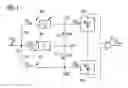
FIG. 1 the basic structure of a DPSK receiver and
FIG. 2 a receive diagram.
DETAILED DESCRIPTION OF INVENTION FIG. 1 shows the basic structure of the DPSK receiver. A differential phase-modulated signal DPS is fed to its input, which is at the same time the input of a first splitter SP1. The splitter SP1 divides this signal into three signal components K1, K2, K3. The larger signal component K1, which is twice as large as the other two signal components K2 or K3, is routed via a first signal path W1 containing a timing element TP for which the runtime with binary DPSKs amounts to half a period of the carrier signal. A second splitter SP2, which divides the signal into two component parts TK1 and TK2, is arranged at the output of this timer. The second signal component K2 is routed via a second signal path W2 into which an adjustable timer TK is connected. The correspondingly delayed second signal component K2 is combined with the component part TK11 in a first combiner CM1. Likewise the second component TK12 is combined in a second combiner CM2 with the third signal component K3 which is routed via the third signal path W3 which in this exemplary embodiment does not contain a timer. The output signals AS1 and AS2 of the combiner CM1 and CM2 are routed via opto-electrical converters PH1 and PH2 (photodiodes) to the differential inputs of a differential amplifier DV, at the output of which a demodulated electrical data signal DS is output. The output signals of the combiners are calculated as
AS1(f)=(e−j2πfτ+e−j2πfT)/2=e−jπf(T+τ) cos(πf(τ−T)) and
AS2(f)=(e−2πjT−1)/2=j·e−jπfT sin(πfT),
with f being the frequency of the carrier signal and T and τ the run times of the timers TP and TK. The attenuation of the receiver can be compensated for by optical amplifiers. Adapting to or compensating for the dispersion is undertaken by the adjustable timer TK.
FIG. 2 shows the general sequence of the “eye opening penalty” (EOP) for an approximately 60 km long transmission link with a dispersion of 17 ps/nm·km for an inventive receiver Novel RX and for a conventional receiver Conventional RX. The small diagram shows the delay time of the adjustable timer TK to obtain an optimum compensation. It should also be added that the second outputs (not shown) of the combiners can also be used for demodulation.
Claims
1.-4. (canceled)
5. A component for an optical differential phase modulated signal in a telecommunication network, comprising:
a first splitter that divides the signal into first, second, and third signal components;
a first signal path that routes the firrst signal component from the first splitter to a second splitter, the second splitter that divides the first signal component into two equal-size component parts;
a second signal path that routes the second signal component from the first splitter;
a third signal path that routes the third signal component from the first splitter;
a first combiner having a first input that receives the first equal-size component part and having a second input that receives the second signal from the second signal path, the first combiner that combines the inputs to form a first optical signal;
a second combiner having a first input that receives the second equal-size component part and having a second input that receives the third signal from the third signal path, the second combiner that combines the inputs to form a second optical signal;
a first timer that has a delay of a half period of a carrier signal and connects to the first signal path; and
an adjustable timer connects to the second signal path.
6. The component according to claim 5, wherein the signal is divided on the signal paths in the ratios 50%, 25%, 25%.
7. The component according to claim 5, wherein the component is a receiver.
8. The receiver in accordance to claim 5, wherein an opto-electrical converter is connected to first and second optical signals, the output of the converter is routed to the input of a differential amplifier.
9. A receiver for an optical differential phase modulated signal, comprising:
a first splitter that divides the signal into first, second, and third signal components, the second and third signal components having equal size, the first splitter arranged on an input side of the receiver;
a first signal path that routes the first signal component from the first splitter to a second splitter, the second splitter that divides the first signal component into two equal-size component parts;
a first combiner having first and second inputs, the first combiner first input that receives the first equal-size component part;
a second combiner having first and second inputs, the second combiner first input that receives the second equal-size component part;
a second signal path that routes the second signal component from the first splitter to the first combiner second input;
a third signal path that routes the third signal component from the first splitter to the second combiner second input;
a first timer that connects to the first signal path; and
a second timer connects to the second signal path,
wherein each combiner outputs an optical signal.
10. The receiver according to claim 9, wherein the signal is divided on the signal paths in the ratios 50%, 25%, 25%.
11. The receiver according to claim 9, wherein the first timer has a delay of a half period of a carrier signal and the second timer is adjustable.
12. The receiver according to claim 10, wherein the first timer runs for a half period of a carrier signal and the second timer is adjustable.
13. The receiver in accordance to claim 9, wherein an opto-electrical converter is connected to the outputs of the first and second combiners, the output of the converter is routed to the input of a differential amplifier.
14. A method for receiving an optical differential phase modulated signal within a telecommunication network, comprising:
splitting the signal first into first, second, and third signal components, the second and third signal components having equal size;
routing the first signal component from the first splitter to a second splitter via a first signal path;
routing the second signal component from the first splitter to a first combiner via a second signal path;
routing the third signal component from the first splitter to a second combiner via a third signal path;
dividing the first signal component into two equal-size component parts;
combining the first equal size component part with the second signal component via the first combiner to form a first optical signal; and
combining the second equal size component part with the third signal component via the second combiner to form a second optical signal,
wherein a first timer has a delay of a half period of the signal for demodulation, and
wherein an adjustable timer is provided in the second signal path to compensate for dispersion.
15. The method according to claim 14, wherein the signal is divided on the signal paths in the ratios 50%, 25%, 25%.
Images & Drawings included:


Sources:
- United States Patent and Trademark Office - verify current appl. status at the USPTO↗
Similar patent applications:
Recent applications in this class:
- » 20250150176 2025-05-08
OPTICAL RECEIVER - » 20250125879 2025-04-17
RECEPTION CONTROL DEVICE, RECEPTION CONTROL METHOD, AND RECORDING MEDIUM - » 20240421913 2024-12-19
Electro-photonic circuit comprising burst-mode optical receiver - » 20240187108 2024-06-06
ELECTRICAL DUOBINARY SOFT INFORMATION RECEIVER FOR NRZ MODULATION FIBER TRANSMISSION - » 20230396342 2023-12-07
OPTICAL RECEIVING APPARATUS, OPTICAL RECEIVING PACKAGING APPARATUS, AND RELATED DEVICE AND METHOD - » 20230261759 2023-08-17
OPTICAL SIGNAL DEMODULATOR, CONTROL METHOD AND PROGRAM - » 20230231632 2023-07-20
Optical device, optical transmission apparatus, optical reception apparatus, and optical communication apparatus - » 20230084591 2023-03-16
DC and offset cancellation for fully differential optical receiver - » 20230054439 2023-02-23
Optical communication device - » 20230013373 2023-01-19
Leveraging coherent detection to measure performance of optical transmitter
Recent applications for this Assignee:
- » 20140287710 2014-09-25
Method for transmission of alarm messages to subscriber terminals in radio communications system - » 20130294286 2013-11-07
Conflict handling in self-organizing networks - » 20130148664 2013-06-13
Method for generating an address field, method and device for transmitting electronic message and data packet - » 20130148551 2013-06-13
Method and apparatus for providing signaling of redundancy - » 20130124939 2013-05-16
Method and device for padding optimization of segmented turbo codes - » 20120233302 2012-09-13
Virtual network controller - » 20110305154 2011-12-15
Transmitting a first and a second channel quality information between two network elements - » 20110295994 2011-12-01
Method and device for operating a group service in a communications network - » 20110164571 2011-07-07
METHOD FOR ESTABLISHING OF A POINT-TO-POINT CONNECTION BETWEEN A MOBILE NODE AND A NETWORK ENTITY, A CORRESPONDING MOBILE NODE AND A CORRESPONDING NETWORK ENTITY - » 20110131474 2011-06-02
Encoding and decoding method, and encoding and decoding devices with a two-stage error protection process