Thin film semiconductor device comprising nanocrystalline silicon powder
US20060199313A1
2006-09-07
10/543,475
2004-01-30
✅ Patent granted
US 8,026,565 B2
2011-09-27
WO; PCT/IB2004/000221; 20040130
WO; WO2004/068536; 20040812
Matthew Landau | Maliheh Malek
2024-07-23
Abstract:
A thin film semiconductor in the form of a metal semiconductor field effect transistor, includes a substrate 10 of paper sheet material and a number of thin film active inorganic layers that are deposited in layers on the substrate. The active layers are printed using an offset lithography printing process. A first active layer comprises source 12.1 and drain 12.2 conductors of colloidal silver ink, that are printed directly onto the paper substrate. A second active layer is an intrinsic semiconductor layer 14 of colloidal nanocrystalline silicon ink which is printed onto the first layer. A third active layer comprises a metallic conductor 16 of colloidal silver which is printed onto the second layer to form a gate electrode. This invention extends to other thin film semiconductors such as photovoltaic cells and to a method of manufacturing semiconductors.
Inventors:
- David Thomas Britton 14 🇿🇦 Cape Town, South Africa
- Margit HARTING 5 🇿🇦 Mowbray, South Africa
Assignee:
- UNIVERSITY OF CAPE TOWN 93 🇿🇦 Cape Town, South Africa
Interested in similar patents?
Get notified when new applications in this technology area are published.
Classification:
H01L31/022425 » CPC main
Semiconductor devices sensitive to infra-red radiation, light, electromagnetic radiation of shorter wavelength or corpuscular radiation and specially adapted either for the conversion of the energy of such radiation into electrical energy or for the control of electrical energy by such radiation; Processes or apparatus specially adapted for the manufacture or treatment thereof or of parts thereof; Details thereof; Details; Electrodes for devices characterised by at least one potential jump barrier or surface barrier for solar cells
H01L21/02422 » CPC further
Processes or apparatus adapted for the manufacture or treatment of semiconductor or solid state devices or of parts thereof; Manufacture or treatment of semiconductor devices or of parts thereof; Forming layers; Forming inorganic semiconducting materials on a substrate; Substrates; Materials Non-crystalline insulating materials, e.g. glass, polymers
H01L21/02488 » CPC further
Processes or apparatus adapted for the manufacture or treatment of semiconductor or solid state devices or of parts thereof; Manufacture or treatment of semiconductor devices or of parts thereof; Forming layers; Forming inorganic semiconducting materials on a substrate; Intermediate layers between substrates and deposited layers; Materials Insulating materials
H01L21/02491 » CPC further
Processes or apparatus adapted for the manufacture or treatment of semiconductor or solid state devices or of parts thereof; Manufacture or treatment of semiconductor devices or of parts thereof; Forming layers; Forming inorganic semiconducting materials on a substrate; Intermediate layers between substrates and deposited layers; Materials Conductive materials
H01L21/02521 » CPC further
Processes or apparatus adapted for the manufacture or treatment of semiconductor or solid state devices or of parts thereof; Manufacture or treatment of semiconductor devices or of parts thereof; Forming layers; Forming inorganic semiconducting materials on a substrate; Deposited layers Materials
H01L29/16 » CPC further
Semiconductor devices adapted for rectifying, amplifying, oscillating or switching, or capacitors or resistors with at least one potential-jump barrier or surface barrier, e.g. PN junction depletion layer or carrier concentration layer; Details of semiconductor bodies or of electrodes thereof; Multistep manufacturing processes therefor; Semiconductor bodies ; Multistep manufacturing processes therefor characterised by the materials of which they are formed including, apart from doping materials or other impurities, only elements of Group IV of the Periodic System
H01L29/66848 » CPC further
Semiconductor devices adapted for rectifying, amplifying, oscillating or switching, or capacitors or resistors with at least one potential-jump barrier or surface barrier, e.g. PN junction depletion layer or carrier concentration layer; Details of semiconductor bodies or of electrodes thereof; Multistep manufacturing processes therefor; Types of semiconductor device ; Multistep manufacturing processes therefor; Multistep manufacturing processes of devices having semiconductor bodies comprising group 14 or group 13/15 materials the devices being controllable only by the electric current supplied or the electric potential applied, to an electrode which does not carry the current to be rectified, amplified or switched, e.g. three-terminal devices; Unipolar field-effect transistors with a Schottky gate, i.e. MESFET
H01L31/03921 » CPC further
Semiconductor devices sensitive to infra-red radiation, light, electromagnetic radiation of shorter wavelength or corpuscular radiation and specially adapted either for the conversion of the energy of such radiation into electrical energy or for the control of electrical energy by such radiation; Processes or apparatus specially adapted for the manufacture or treatment thereof or of parts thereof; Details thereof characterised by their semiconductor bodies characterised by their crystalline structure or particular orientation of the crystalline planes including thin films deposited on metallic or insulating substrates ; characterised by specific substrate materials or substrate features or by the presence of intermediate layers, e.g. barrier layers, on the substrate including only elements of Group IV of the Periodic System
H01L31/046 » CPC further
Semiconductor devices sensitive to infra-red radiation, light, electromagnetic radiation of shorter wavelength or corpuscular radiation and specially adapted either for the conversion of the energy of such radiation into electrical energy or for the control of electrical energy by such radiation; Processes or apparatus specially adapted for the manufacture or treatment thereof or of parts thereof; Details thereof adapted as photovoltaic [PV] conversion devices; PV modules or arrays of single PV cells including thin film solar cells, e.g. single thin film a-Si, CIS or CdTe solar cells PV modules composed of a plurality of thin film solar cells deposited on the same substrate
H01L31/202 » CPC further
Semiconductor devices sensitive to infra-red radiation, light, electromagnetic radiation of shorter wavelength or corpuscular radiation and specially adapted either for the conversion of the energy of such radiation into electrical energy or for the control of electrical energy by such radiation; Processes or apparatus specially adapted for the manufacture or treatment thereof or of parts thereof; Details thereof; Processes or apparatus specially adapted for the manufacture or treatment of these devices or of parts thereof such devices or parts thereof comprising amorphous semiconductor materials including only elements of Group IV of the Periodic System
Y02E10/50 » CPC further
Energy generation through renewable energy sources Photovoltaic [PV] energy
Y02E10/50 » CPC further
Energy generation through renewable energy sources Photovoltaic [PV] energy
Y02P70/50 » CPC further
Climate change mitigation technologies in the production process for final industrial or consumer products Manufacturing or production processes characterised by the final manufactured product
Y02P70/50 » CPC further
Climate change mitigation technologies in the production process for final industrial or consumer products Manufacturing or production processes characterised by the final manufactured product
Y10S977/775 » CPC further
Nanotechnology; Nanostructure; Nanoparticle, i.e. structure having three dimensions of 100 nm or less Nanosized powder or flake, e.g. nanosized catalyst
Y10S977/778 » CPC further
Nanotechnology; Nanostructure within specified host or matrix material, e.g. nanocomposite films
Y10S977/785 » CPC further
Nanotechnology; Nanostructure within specified host or matrix material, e.g. nanocomposite films Electrically insulating host material
H01L21/84 IPC
Processes or apparatus adapted for the manufacture or treatment of semiconductor or solid state devices or of parts thereof; Manufacture or treatment of devices consisting of a plurality of solid state components formed in or on a common substrate or of parts thereof; Manufacture of integrated circuit devices or of parts thereof; Manufacture or treatment of devices consisting of a plurality of solid state components or integrated circuits formed in, or on, a common substrate with subsequent division of the substrate into plural individual devices to produce devices, e.g. integrated circuits, each consisting of a plurality of components the substrate being other than a semiconductor body, e.g. being an insulating body
H01L23/02 IPC
Details of semiconductor or other solid state devices Containers; Seals
B82Y20/00 IPC
Nanooptics, e.g. quantum optics or photonic crystals
Description
FIELD OF INVENTIONTHIS INVENTION relates to a thin film semiconductor device.
It also relates to a method of manufacturing a thin film semiconductor device.
BACKGROUND OF INVENTIONSemiconductor devices currently in production or under commercial development, can be classified in three categories: single crystalline silicon, bulk polycrystalline silicon or thin film semiconductor. The first two are expensive to produce and are aimed at the high end of the market. Most research and development is aimed at improving the efficiency and long-term stability of such devices with little regard to cost.
On the other hand, thin film semiconductors are generally intended for lower cost applications, where absolute efficiency and compactness is not a prerequisite. Long-term stability is still a desirable goal for existing thin film semiconductors because of the relatively high production costs and the high material costs of the substrate.
Most commercial thin films semiconductor devices are based on hydrogenated amorphous silicon (a-Si:H) which may also contain nanocrystalline or microcrystalline phases deposited by various chemical vapour deposition (CVD) processes. The two main techniques are plasma enhanced CVD (PECVD) also know as glow discharge CVD and catalytic CVD (cat-CVD) also known as hot wire CVD (HWCVD). In the case of photovoltaic semiconductor devices, all CVD deposited thin film semiconductors and a-Si:H, in particular, suffer from light induced degradation (referred to as “the Staebler-Wronksi effect”) which is most significant over the first few years of operation. Consequently, all commercial photovoltaic semiconductor devices are over-engineered so that they degrade according to the specification and are consequently fitted with regulators to keep the output voltage constant. In commercial semiconduction based solar cells, the substrate is typically glass which limits the size of the semiconductor device due to its mechanical stability and weight. Glass also has the added disadvantage of being rigid and brittle.
All commercial thin film transistors (TFT) are based on CVD deposited semiconductor films and involve extensive use of photolithography, masks and chemical etching. In high density transistor arrays, a vertical stacking sequence of different semiconductor layers is used. The deposition techniques for depositing the various semiconductor layers, including for the gate electrodes, are the same as for semiconduction based solar cells and the usual substrate is glass.
A major factor limiting the production of inexpensive semiconductor devices, is the use of vacuum deposition processes in the production. Such vacuum deposition processes are relatively expensive and as such, add significantly to the cost of producing semiconductor devices. Further, semiconductor layers deposited using CVD processes are relatively rigid and as such, do not combine well with flexible substrates.
SUMMARY OF INVENTIONAccording to a first aspect of the invention there is provided a thin film semiconductor device including
a substrate; and
thin film active layers of inorganic material that are deposited in layers on the substrate, wherein at least one active layer is printed onto the substrate or an underlying active layer.
Any reference herein to an “active layer” must be interpreted to include a reference to a semiconductor layer, an insulator layer and metallic contacts.
The active layer may be printed using a transfer printing process selected from a group consisting of offset lithography printing, block printing, letterpress printing and screenprinting using colloidal inks.
The substrate may be of a material including cellulose. More particularly, the substrate may be of paper sheet material.
The semiconductor device may include an active layer comprising a colloidal ink which includes an inorganic semiconductor material powder suspended in a solvent/binder carrier composition.
Each of the active layers may be printed onto one of an underlying active layer and the substrate.
The semiconductor device may be in the form of a photovoltaic cell.
The semiconductor device may be in the form of a field effect transistor.
According to a second aspect of the invention there is provided a method of manufacturing a thin film semiconductor device, including depositing a number of thin film active layers of inorganic material, wherein at least one active layer is printed onto one of the substrate and an underlying active layer.
Said one active layer may be printed using a transfer printing process selected from a group consisting of offset lithography printing, block printing, letterpress printing and screen printing using colloidal inks.
The method may include printing each active layer onto one of the substrate and an underlying active layer.
The method may include printing an active layer in the form of a colloidal ink which includes an inorganic semiconductor material powder suspended in a solvent/binder carrier composition, onto one of a substrate and an underlying active layer.
Any reference herein to “printing” an active layer onto a surface, must be interpreted sufficiently broadly to include coating methods such as spraying, brushing or spin coating an active layer onto a surface, i.e. methods in which no chemical or physical phase change of the coating material occurs during deposition.
Further features of the invention are described hereinafter by way of a non-limiting example of the invention, with reference to and as illustrated in the accompanying diagrammatic drawings. In the drawings:
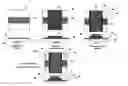
FIG. 1 shows cross-sections and top plan views showing the configuration of the various layers of a top gate metal semiconductor field effect transistor (MS-FET) according to a first example of the invention;
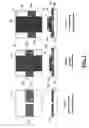
FIG. 2 shows cross-sections and top plan views showing the configuration of the various layers of a bottom gate MS-FET according to a second example of the invention;
FIG. 3 shows a cross-section and top plan view showing the configuration of the various layers of a photovoltaic cell in accordance with a third example of the invention; and
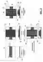
FIG. 4 shows a top plan view and cross-section showing the configuration of a photovoltaic battery in accordance with a fourth example of the invention;
EXAMPLE 1FIG. 1 shows a top gate MS-FET comprising three thin film semiconductor layers which are supported on a substrate 10 of paper sheet. The Applicant has found plain office paper such as Mondi Rotatrim wood free office paper, having a density of 80 g/m2, to be suitable for the purpose. The first active layer comprises two spaced metallic conductors of, for example, colloidal silver such as Dupont Luxprint 5000, which comprises the source 12.1 and drain 12.2 of the field effect transistor. The metallic conductors forming the source and drain are printed directly onto the paper substrate 10 using an offset lithograph printing process.
The source and drain contacts have layer thicknesses of 300-400 microns.
The second semiconductor layer is an intrinsic semiconductor layer 14 of colloidal nanocrystalline silicon (nc-Si) ink which is printed onto the first layer using an offset lithography printing process. The colloidal nc-Si material forming the semiconductor layer 14 is produced using 30 mm diameter intrinsic silicon powder in a solvent-binder carrier. The applicant has found that other semiconductor nanopowders, for example, silicon carbide, cadmium sulphide, can be used for other applications. For example, doped semiconductor layers can be produced by replacing the intrinsic nanosilicon powder with doped nanosilicon material. The relative concentrations of the component substances in the nc-Si ink which is used to form the semiconductor layer 14, are determined by the viscosity of the ink required in the printing process. In this example, the solvent-binder carrier is a mixture of a polystyrene binder and chloroform as solvent. Other polymer binders which can be used include biopolymers such as cellulose acetate butyrate (CAB) in a variety of solvents such as ether and commercial lacquer thinners. The semiconductor layer 14 has a thicknesses of the order of 1-2 microns when a polystyrene binder and an offset lithography printing process is used.
The third active layer is in the form of a metallic conductor 16 of, for example, colloidal silver material such as Dupont Luxprint 5000, which is printed onto the second layer to form a gate electrode using an offset lithography printing process. Typically, the third layer has a thickness of between 300 and 400 microns.
The top gate MS-FET has a “cross” geometry wherein the top and bottom contacts extend at right angles to one another and can thus be connected directly into the interconnects. As such, this allows the interconnects to also be printed, either at the same time or subsequently if different layers are connected, making the production process simpler and cheaper.
The Applicant envisages that offset lithography printing will be used for printing the various semiconductor layers in the commercial production of semiconductor devices. However, the Applicant believes that various other printing techniques such as blockprinting, screenprinting, letterpress printing, relief printing, stamp printing, gravure printing and “printing” by spraying, brushing or spin coating a colloidal ink onto a substrate/active layer can also be used. The Applicant envisages further that an array of semiconductor devices similar to the MS-FET described in Example 1, can be produced in a standard threecolour printing run. More elaborate heterostructures, including doped semiconductor layers can be produced by extending the number of “colours” in the printing process.
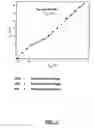
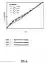
With reference to FIG. 5 of the drawings, the current-voltage characteristics of a prototype top gate MS-FET manufactured by the Applicant in accordance with the invention, are illustrated. The prototype MS-FET tested was equivalent to the top gate MS-FET described in Example 1, with the only difference being that the various active layers were block printed instead of being printed in an offset lithography printing process.
EXAMPLE 2FIG. 2 shows a bottom gate MS-FET comprising three thin film semiconductor layers which are supported on a substrate 10 of paper sheet. The bottom gate MS-FET is the same as the top gate MS-FET illustrated in FIG. 1, with the only difference being that the semiconductor layers have been reversed to form a bottom gate field effect transistor. This allows direct connection of other active components to the source and drain of the transistor for faster switching. The same reference numerals are used in FIG. 2 to designate features of the bottom gate MS-FET that are the same as those of the top gate MS-FET shown in FIG. 1. In this example, the same printing process and material used in the top gate MS-FET of Example 1, is used for the various semiconductor layers.
With reference to FIG. 6 of the drawings, the current-voltage characteristics of a prototype bottom gate MS-FET manufactured by the Applicant in accordance with the invention, are illustrated. The prototype MS-FET tested was equivalent to the bottom gate MS-FET described in Example 2, with the only difference being that the various active layers were block printed instead of being printed in an offset lithography printing process.
EXAMPLE 3With reference to FIG. 3 of the drawings, a thin film semiconductor in the form of a photovoltaic cell 40 is shown which comprises an intrinsic semiconductor 24 (layer 2) sandwiched between two electrodes. More particularly, the photovoltaic cell comprises a first active layer in the form of a metallic base contact 22 of, for example, colloidal silver that is printed onto a major surface of a paper substrate 20 of plain white office paper such as Mondi Rotatrim wood free paper. The second active layer in the form an intrinsic semiconductor, is applied to the first layer. The second layer comprises, for example, colloidal nc-Si which is printed onto the first layer. A third active layer which forms a top contact is a transparent p-type conductor 26, for example, of colloidal indium tin oxide (ITO) such as Dupont Luxprint 7162E translucent conductor material, which is printed onto the second layer. The fourth layer which is optional, is in the form of a clear protective coating 28 of dielectric material such as a clear lacquer, which is printed onto the third layer.
The first and second layers are produced in the same manner as is described in Example 1 for the top gate MS-FET. The third layer is applied using an offset lithography printing process, however, the Applicant has successfully applied the third layer using block printing and brushing techniques in prototype semiconductor structures.
EXAMPLE 4This example shows a construction of a photovoltaic battery which comprises three layers which are deposited onto a paper substrate 20. The battery comprises three photovoltaic cells 40 which are connected in series. The first layer is in the form of a printed metallic base contact 50, for example, of colloidal silver which is printed onto the paper substrate 10. The second layer comprises a single intrinsic semiconductor layer or a semiconductor structure in n-i-p sequence comprising, for example, a colloidal nc-Si layer that is printed onto the first layer. The photovoltaic battery includes a third layer comprising a transparent top contact 54 of, for example, colloidal ITO, that is printed onto the second layer. It will be appreciated that individual battery cells are laid down as strips across the paper substrate 10 by overlapping the top and bottom contacts of neighbouring strips, the cells are automatically connected together in series.
Only two external connections are then required: one at the base contact and one at the top contact. The various semiconductor layers are applied in a three or four colour offset lithography or letterpress printing process.
The open circuit voltage is the product of the number of strips times the cell emf. The width W of the strip determines the area of each cell and therefore for constant current density, the current produced. As such, the length L of the strip determines the number of cells in series and therefore the voltage across the battery.
The Applicant has found that paper fulfils all the necessary requirements for a cheap, robust and flexible substrate. With paper being hygroscopic, the Applicant envisages that it will be necessary to provide a water-resistant seal to protect the paper substrate against degradation due to the ingress of water. It is envisaged by the Applicant that this can be achieved with a varnish which would have to be transparent in the case of use in a solar cell or by keeping the device in a glass cabinet.
The Applicant envisages that a low cost solar cell device which can be replaced after several years of use, can be produced in accordance with the invention. Such low cost solar cell devices can also be used for disposable products such as trickle chargers and power supplies for cell phones and portable computers which make use of ambient light. The Applicant envisages that in such low cost solar cell devices, electrical connections can be made directly to the paper substrate either by crocodile clips or screws. The Applicant envisages further that the whole solar cell structure, with the exception of the external electrical connections, can be protected by a clear varnish which can also be printed onto the structure. For further protection from the external environment, the solar cell should be mounted in a glass cabinet.
The Applicant envisages further that TFT arrays using paper sheet substrates will have advantages over existing TFT arrays with regard to cost, flexibility and robustness for many applications. It is envisaged that in future developments, it will be possible to integrate a TFT array with any of the following display technologies on the same paper substrate to produce an integrated medium resolution display: crystal polymer, electroluminescent phosphors and e-Ink.
Claims
1-16. (canceled)
17. A thin film semiconductor device including:
a substrate comprising a material including cellulose; and
a number of thin film active layers of inorganic material deposited in layers on the substrate, wherein at least one active layer is printed onto one of the substrate and an underlying active layer, and wherein at least one active layer comprises a nanocrystalline silicon powder and a carrier comprising a biopolymer.
18. A thin film semiconductor device according to claim 17 wherein the substrate comprises paper sheet.
19. A thin film semiconductor device according to claim 17 wherein the carrier comprises cellulose acetate butyrate.
20. A thin film semiconductor device according to claim 19 wherein said at least one active layer is printed using an ink comprising said nanocrystalline silicon powder, said carrier comprising cellulose acetate butyrate, and a solvent.
21. A thin film semiconductor device according to claim 20 wherein the solvent comprises ether or lacquer thinners.
22. A thin film semiconductor device according to claim 17 including a transparent water-resistant seal.
23. A thin film semiconductor device according to claim 20 wherein the water resistant seal comprises a clear varnish or lacquer printed onto the device.
24. A semiconductor device according to claim 17, wherein the active layer is printed using a transfer printing process selected from a group consisting of offset lithography printing, block printing, stamp printing, relief printing, gravure printing, letterpress printing and screenprinting using colloidal inks.
25. A semiconductor device according to claim 17, wherein each of the active layers is printed onto one of an underlying active layer and substrate.
26. A semiconductor device according to claim 17, which is in the form of a photovoltaic cell.
27. A semiconductor device according to claim 26 wherein the photovoltaic cell comprises a first layer in the form of a metallic contact printed onto a major surface of the substrate, a second, active layer comprising nanocrystalline silicon applied to the contact, and a third layer defining a transparent contact printed onto the active layer.
28. A semiconductor device according to claim 27 wherein the second, active layer comprises an intrinsic semiconductor and the third layer comprises a p-type semiconductor.
29. A semiconductor device according to claim 27 wherein the second, active layer comprises a semiconductor structure in n-i-p sequence.
30. A semiconductor device according to claim 27 including a fourth layer comprising a clear protective coating of dielectric material printed onto the third layer.
31. A semiconductor device according to claim 30 wherein the protective coating comprises a clear lacquer.
32. A semiconductor device according to claim 27 comprising a plurality of photovoltaic cells connected in series, each photovoltaic cell being formed adjacent to at least one other photovoltaic cell, with the third layer of at least one cell, defining a transparent contact thereof, overlapping the first layer of an adjacent cell, defining a metallic contact thereof, thereby connecting the adjacent cells electrically in series.
33. A power supply comprising at least one semiconductor device according to claim 32.
34. A semiconductor device according to claim 17, which is in the form of a field effect transistor.
35. A semiconductor device according to claim 34 wherein the field effect transistor includes a first layer defining metallic source and drain contacts printed onto the substrate, a second layer comprising nanocrystalline silicon applied to the first layer, and a third layer defining a metallic gate electrode printed onto the second layer.
36. A semiconductor device according to claim 35 wherein the source and drain contacts of the first layer and the gate electrode of the third layer extend at right angles to one another to define a “cross” geometry.
37. A semiconductor device according to claim 34 wherein the field effect transistor includes a first layer defining a gate contact printed onto the substrate, a second layer comprising nanocrystalline silicon applied to the first layer, and a third layer defining metallic source and drain contacts printed onto the second layer.
38. A semiconductor device according to claim 37 wherein the gate contact of the first layer and the source and drain contacts of the third layer extend at right angles to one another to define a “cross” geometry.
39. A method of manufacturing a thin film semiconductor device, which includes depositing a number of thin film active layers of inorganic material onto a substrate comprising a material including cellulose, wherein at least one active layer is printed onto one of the substrate and an underlying active layer, and wherein at least one active layer comprises a nanocrystalline silicon powder and a carrier comprising a biopolymer.
40. A method according to claim 39 wherein at least one active layer is printed using a transfer printing process selected from a group consisting of offset lithography printing, block printing, stamp printing, relief printing, gravure printing, letterpress printing and screen printing using colloidal inks.
41. A method according to claim 39 wherein each active layer is printed onto one of the substrate and an underlying active layer.
42. A method according to claim 39 wherein each active layer is applied in a three or four colour lithographic printing process.
Images & Drawings included:


Sources:
- United States Patent and Trademark Office - verify current appl. status at the USPTO↗
Recent applications in this class:
- » 20250006851 2025-01-02
FRONT CONTACT SOLAR CELL WITH FORMED EMITTER - » 20240429328 2024-12-26
Method of deposition on a substrate used for the manufacture of a solar cell, screen for screen printing on a substrate used for the manufacture of a solar cell, processing line for processing a substrate used for the manufacture of a solar cell - » 20240429327 2024-12-26
SOLAR CELL AND METHOD FOR PRODUCING THE SOLAR CELL - » 20240395954 2024-11-28
SOLAR CELL AND MANUFACTURING METHOD THEREOF, PHOTOVOLTAIC MODULE AND PHOTOVOLTAIC SYSTEM - » 20240304737 2024-09-12
SOLAR CELL UPPER ELECTRODE AND MANUFACTURING METHOD THEREFOR - » 20240290895 2024-08-29
Electrode paste in contact with p+ emitter of N-type solar cell - » 20240274730 2024-08-15
PHOTOELECTRIC CONVERSION ELEMENT, METHOD FOR MANUFACTURING PHOTOELECTRIC CONVERSION ELEMENT, SOLAR CELL MODULE, AND PADDLE - » 20240213381 2024-06-27
SOLAR CELL AND PHOTOVOLTAIC MODULE - » 20240204117 2024-06-20
SOLAR CELL AND MANUFACTURING METHOD THEREFOR - » 20240178330 2024-05-30
SYSTEMS AND METHOD FOR MANUFACTURING SOLAR CELL PASTE
Recent applications for this Assignee:
- » 20250197874 2025-06-19
PLANT-PRODUCED CHIMAERIC ORBIVIRUS VLPS - » 20240376546 2024-11-14
TARGETS OVEREXPRESSED ON THE SURFACE OF CANCER CELLS - » 20240369554 2024-11-07
METHOD OF DETECTING AND IDENTIFYING A MICROORGANISM - » 20240307051 2024-09-19
Implantable device - » 20240287534 2024-08-29
INTEGRATED MOLECULAR AND GLYCO-ENGINEERING OF COMPLEX VIRAL GLYCOPROTEINS - » 20240271147 2024-08-15
TOBAMOVIRUS PSEUDOVIRIONS FOR STABILISING SINGLE STRANDED RNA - » 20220412824 2022-12-29
GROUND REACTION FORCE PLATE APPARATUS AND MEASUREMENT SYSTEM - » 20220273480 2022-09-01
KNEE BRACE - » 20220204987 2022-06-30
Drought resistance multigene construct - » 20220158451 2022-05-19
Frequency domain-based determination of currents for injection into a power network