Three-transistor CMOS active pixel
US20060203114A1
2006-09-14
11/075,431
2005-03-08
Abstract:
A CMOS image sensor includes a plurality of pixels defining an imaging area each pixel includes a photosensitive area that converts incident light into a charge; a first transistor having a transfer gate that transfers charge from the photosensitive area to a charge-to-voltage region; a second transistor that resets the voltage of the charge-to-voltage region; a third transistor that amplifies voltage from the charge-to-voltage region; and a select mechanism positioned outside the imaging area on the image sensor that selects a predefined number of pixels for readout from the third transistor.
Interested in similar patents?
Get notified when new applications in this technology area are published.
Classification:
H04N3/155 » CPC main
Scanning details of television systems; Combination thereof with generation of supply voltages by means not exclusively optical-mechanical by means of electrically scanned solid-state devices for picture signal generation Control of the image-sensor operation, e.g. image processing within the image-sensor
H01L27/14609 » CPC further
Devices consisting of a plurality of semiconductor or other solid-state components formed in or on a common substrate including semiconductor components sensitive to infra-red radiation, light, electromagnetic radiation of shorter wavelength or corpuscular radiation and specially adapted either for the conversion of the energy of such radiation into electrical energy or for the control of electrical energy by such radiation; Devices controlled by radiation; Imager structures; Structural or functional details thereof Pixel-elements with integrated switching, control, storage or amplification elements
H04N5/3741 » CPC further
Details of television systems; Transforming light or analogous information into electric information using solid-state image sensors [SSIS]; SSIS architecture; Circuitry associated therewith; Addressed sensors, e.g. MOS or CMOS sensors comprising control or output lines sharing a plurality of functions, e.g. output or driving or reset or power lines
H04N5/335 IPC
Details of television systems; Transforming light or analogous information into electric information using solid-state image sensors [SSIS]
H04N3/14 IPC
Scanning details of television systems; Combination thereof with generation of supply voltages by means not exclusively optical-mechanical by means of electrically scanned solid-state devices
H01L31/113 IPC
Semiconductor devices sensitive to infra-red radiation, light, electromagnetic radiation of shorter wavelength or corpuscular radiation and specially adapted either for the conversion of the energy of such radiation into electrical energy or for the control of electrical energy by such radiation; Processes or apparatus specially adapted for the manufacture or treatment thereof or of parts thereof; Details thereof in which radiation controls flow of current through the device, e.g. photoresistors characterised by at least one potential-jump barrier or surface barrier, e.g. phototransistors; Devices sensitive to infra-red, visible or ultra-violet radiation characterised by field-effect operation, e.g. junction field-effect phototransistor being of the conductor-insulator-semiconductor type, e.g. metal-insulator-semiconductor field-effect transistor
H01L31/062 IPC
Semiconductor devices sensitive to infra-red radiation, light, electromagnetic radiation of shorter wavelength or corpuscular radiation and specially adapted either for the conversion of the energy of such radiation into electrical energy or for the control of electrical energy by such radiation; Processes or apparatus specially adapted for the manufacture or treatment thereof or of parts thereof; Details thereof adapted as photovoltaic [PV] conversion devices characterised by at least one potential-jump barrier or surface barrier the potential barriers being only of the metal-insulator-semiconductor type
Description
FIELD OF THE INVENTIONThe invention relates generally to the field of CMOS image sensors and, more particularly, to such CMOS image sensors having a three-transistor design with substantially the same sensitivity of a four-transistor design.
BACKGROUND OF THE INVENTIONWith the size of image sensors (the number of pixels) increasing rapidly, smaller pixel size is highly desired. The typical pixels of a CMOS image sensor are either the three- or four-transistor design. The three-transistor design has the desired smaller size but with an undesirable noise level as compared to the four-transistor design. The four-transistor design has higher sensitivity than the three-transistor design, but it obviously occupies a larger spatial area, which is undesirable, and the additional couplings inherent in such a design creates more noise as the pixel size shrinks.
Consequently, a need exists for a pixel of a CMOS transistor to have the sensitivity of the four-transistor design and the size of the three-transistor design.
SUMMARY OF THE INVENTIONThe present invention is directed to overcoming one or more of the problems set forth above. Briefly summarized, according to one aspect of the present invention, the invention resides in a CMOS image sensor comprising a plurality of pixels defining an imaging area each pixel comprising (a) a photosensitive area that converts incident light into a charge; (b) a first transistor having a transfer gate that transfers charge from the photosensitive area to a charge-to-voltage region; (c) a second transistor that resets the voltage of the charge-to-voltage region; (d) a third transistor that amplifies voltage from the charge-to-voltage region; and a select mechanism positioned outside the imaging area on the image sensor that selects a predefined number of pixels for readout from the third transistor.
These and other aspects, objects, features and advantages of the present invention will be more clearly understood and appreciated from a review of the following detailed description of the preferred embodiments and appended claims, and by reference to the accompanying drawings.
Advantageous Effect of the Invention
The present invention has the following advantage of a three-transistor CMOS image sensor with the sensitivity of a four-transistor design.
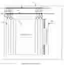
BRIEF DESCRIPTION OF THE DRAWINGSFIG. 1 is a top view of the image sensor of the present invention;
FIG. 2 is a top, detailed view of a typical pixel of FIG. 1; and
FIG. 3 is the typical timing diagram associated for FIG. 2.
DETAILED DESCRIPTION OF THE INVENTIONReferring to FIG. 1, there is shown a top view of the CMOS image sensor 10 of the present invention. The image sensor 10 includes an imaging area 20 having a plurality of pixels 30 that defines a boundary for an array of pixels. A plurality of switches 40 is positioned on the CMOS image sensor 10 outside the boundary of the imaging area 20. Each switch 40 is connected to a power supply bus 50 that permits the row of pixels to be selected for readout when the switch 40 is closed as will be discussed in detail hereinbelow. A voltage from each pixel of the row of pixels is then readout to a sample and hold circuit 45, also positioned outside the imaging area 20, for further processing as is well known in the art.
Referring to FIGS. 2 and 3, there are shown a detailed view of a representative pixel 30 of the present invention and its associated timing diagram. Each pixel 30 includes a photodiode or photosensitive area 60 that converts incident light into a charge. A transistor 70 is electrically connected to the photodiode 60 and includes a transfer gate 80 that, when pulsed, permits the charge to pass from the photodiode 60 to a charge-to-voltage conversion region 90, a floating diffusion in the preferred embodiment. A capacitor 100 is electrically connected to the floating diffusion for facilitating the charge-to-voltage conversion by the floating diffusion 90.
A reset transistor 110 is electrically connected to the node of the floating diffusion 90 for resetting the voltage of the floating diffusion 90. In this regard, to reset the voltage of the floating diffusion 90, the row select switch 40 is closed to enable the row of pixels and the reset gate 120 is pulsed for resetting the floating diffusion 90 to the voltage of Vdd or substantially close to the voltage of Vdd. It is noted that a ground or disable switch 125, which is connected to a ground bus 55, is always in the opposite position as switch 40 for preventing leaking current.
The gate 130 of an amplifying transistor 140 is electrically connected to the floating diffusion 90 for receiving and amplifying the voltage of the floating diffusion 90. The amplifying transistor 140 receives the reset voltage and transfers to the output 150 when the reset transistor 110 is pulsed, as discussed in the preceding paragraph. Then the amplifying transistor 140 receives and transfers the image signal to the output 150 when the transfer gate 80 of the transfer transistor 70 is pulsed, which dumps the charge onto the floating diffusion 90 that consequently is read as a voltage by the amplifying transistor 140, as also discussed above. A bias current 160 is connected to the output of the amplifier for biasing the amplifier.
The output of the amplifier is then readout to a sample and hold circuit array 45 (see FIG. 1).
The invention has been described with reference to a preferred embodiment. However, it will be appreciated that variations and modifications can be effected by a person of ordinary skill in the art without departing from the scope of the invention.
PARTS LIST
- 10 image sensor
- 20 imaging area/pixel array
- 30 pixels
- 40 switches
- 45 sample and hold circuit/circuit array
- 50 power supply bus
- 55 ground bus
- 60 photosensitive area/photodiode
- 70 transfer gate transistor
- 80 transfer gate
- 90 charge-to-voltage conversion region/floating diffusion
- 100 floating diffusion capacitor
- 110 reset transistor
- 120 reset gate
- 125 ground or disable switch
- 130 gate of the amplifying transistor
- 140 amplifying transistor
- 150 pixel output
- 160 bias current
Claims
1. A CMOS image sensor comprising:
a plurality of pixels defining an imaging area each pixel comprising:
(a) a photosensitive area that converts incident light into a charge;
(b) a first transistor having a transfer gate that transfers charge from the photosensitive area to a charge-to-voltage conversion region;
(c) a second transistor that resets the voltage of the charge-to-voltage conversion region;
(d) a third transistor that amplifies voltage from the charge-to-voltage region; and
(e) a select mechanism positioned outside the imaging area that selects a predefined number of pixels for readout from the third transistor.
2. The CMOS image sensor as in claim 1, wherein the select mechanism is a switch.
3. The CMOS image sensor as in claim 1, wherein the predefined number of pixels is a row of pixels.
4. The CMOS image sensor as in claim 2, wherein the predefined number of pixels is a row of pixels.
5. The CMOS image sensor as in claim 1, wherein the charge-to-voltage conversion region is a floating diffusion.
6. The CMOS image sensor as in claim 5 further comprising a capacitor connected to a node of the floating diffusion.
7. The CMOS image sensor as in claim 3, wherein the select mechanism is a switch.
8. The CMOS image sensor as in claim 1, further comprising a plurality of select mechanisms each operating a predefined number of pixels.
9. The CMOS image sensor as on claim 8, wherein a row of pixels is the predefined number of pixels.
10. The CMOS image sensor as in claim 8, wherein the plurality of select mechanisms are a plurality of switches with each switch operating a predefined number of pixels.
11. The CMOS image sensor as in claim 10, wherein the predefined number of pixels are a row of pixels.
Images & Drawings included:


Sources:
- United States Patent and Trademark Office - verify current appl. status at the USPTO↗
Recent applications in this class:
- » 20210227099 2021-07-22
Touch accommodation options - » 20190394359 2019-12-26
Image sensors including ripple voltage compensation - » 20190364173 2019-11-28
Touch accommodation options - » 20190281192 2019-09-12
Imaging device and imaging system - » 20180213126 2018-07-26
TOUCH ACCOMMODATION OPTIONS - » 20180103182 2018-04-12
Imaging device and imaging system - » 20170359492 2017-12-14
Image sensors including ripple voltage compensation - » 20160094760 2016-03-31
IMAGING DEVICE AND METHOD FOR HIGH-SENSITIVITY OPTICAL SCANNING AND INTEGRATED CIRCUIT THEREFOR - » 20160037020 2016-02-04
Detecting transient signals using stacked-chip imaging systems - » 20160014304 2016-01-14
Solid-state imaging device