Semiconductor optical element
US20060220037A1
2006-10-05
11/263,997
2005-11-02
✅ Patent granted
US 7,259,406 B2
2007-08-21
-
-
Ida M. Soward
2026-04-15
Abstract:
A semiconductor optical element having a includes an n-type GaAs buffer layer, an n-type AlGaInP cladding layer, a first InGaAsP (including zero As content) guide layer without added dopant impurities, an InGaAsP (including zero In content) active layer, a second InGaAsP (including zero As content) guide layer without added dopant impurities, a p-type AlGaInP cladding layer, a p-type band discontinuity reduction layer, and a p-type GaAs contact layer sequentially laminated on an n-type GaAs substrate C or Mg is the dopant impurity in the p-type-GaAs contact layer, the p-type band discontinuity reduction layer, and the p-type AlGaInP cladding layer.
Inventors:
- Kimio SHIGIHARA 37 🇯🇵 Tokyo, Japan
- Kimitaka Shibata 5 🇯🇵 Tokyo, Japan
- Yoshihiko Hanamaki 17 🇯🇵 Tokyo, Japan
- Kazushige Kawasaki 34 🇯🇵 Tokyo, Japan
- Kenichi Ono 39 🇯🇵 Tokyo, Japan
- Naoyuki Shimada 4 🇯🇵 Tokyo, Japan
Assignee:
- MITSUBISHI DENKI KABUSHIKI KAISHA 2,997 🇯🇵 Tokyo, Japan
Interested in similar patents?
Get notified when new applications in this technology area are published.
Classification:
H01L29/06 IPC
Semiconductor devices adapted for rectifying, amplifying, oscillating or switching, or capacitors or resistors with at least one potential-jump barrier or surface barrier, e.g. PN junction depletion layer or carrier concentration layer; Details of semiconductor bodies or of electrodes thereof; Multistep manufacturing processes therefor; Semiconductor bodies ; Multistep manufacturing processes therefor characterised by their shape; characterised by the shapes, relative sizes, or dispositions of the semiconductor regions ; characterised by the concentration or distribution of impurities within semiconductor regions
H01S5/22 » CPC main
Semiconductor lasers; Structure or shape of the semiconductor body to guide the optical wave ; Confining structures perpendicular to the optical axis, e.g. index or gain guiding, stripe geometry, broad area lasers, gain tailoring, transverse or lateral reflectors, special cladding structures, MQW barrier reflection layers having a ridge or stripe structure
H01S5/323 » CPC further
Semiconductor lasers; Structure or shape of the active region; Materials used for the active region comprising PN junctions, e.g. hetero- or double- heterostructures in AB compounds, e.g. AlGaAs-laser, InP-based laser
H01L31/12 IPC
Semiconductor devices sensitive to infra-red radiation, light, electromagnetic radiation of shorter wavelength or corpuscular radiation and specially adapted either for the conversion of the energy of such radiation into electrical energy or for the control of electrical energy by such radiation; Processes or apparatus specially adapted for the manufacture or treatment thereof or of parts thereof; Details thereof structurally associated with, e.g. formed in or on a common substrate with, one or more electric light sources, e.g. electroluminescent light sources, and electrically or optically coupled thereto
H01L29/24 IPC
Semiconductor devices adapted for rectifying, amplifying, oscillating or switching, or capacitors or resistors with at least one potential-jump barrier or surface barrier, e.g. PN junction depletion layer or carrier concentration layer; Details of semiconductor bodies or of electrodes thereof; Multistep manufacturing processes therefor; Semiconductor bodies ; Multistep manufacturing processes therefor characterised by the materials of which they are formed including, apart from doping materials or other impurities, only semiconductor materials not provided for in groups
H01L33/00 IPC
Semiconductor devices with at least one potential-jump barrier or surface barrier specially adapted for light emission; Processes or apparatus specially adapted for the manufacture or treatment thereof or of parts thereof; Details thereof
H01L29/12 IPC
Semiconductor devices adapted for rectifying, amplifying, oscillating or switching, or capacitors or resistors with at least one potential-jump barrier or surface barrier, e.g. PN junction depletion layer or carrier concentration layer; Details of semiconductor bodies or of electrodes thereof; Multistep manufacturing processes therefor; Semiconductor bodies ; Multistep manufacturing processes therefor characterised by the materials of which they are formed
H01L31/0328 IPC
Semiconductor devices sensitive to infra-red radiation, light, electromagnetic radiation of shorter wavelength or corpuscular radiation and specially adapted either for the conversion of the energy of such radiation into electrical energy or for the control of electrical energy by such radiation; Processes or apparatus specially adapted for the manufacture or treatment thereof or of parts thereof; Details thereof characterised by their semiconductor bodies characterised by the material; Inorganic materials including, apart from doping materials or other impurities, semiconductor materials provided for in two or more of groups -
Description
BACKGROUND OF THE INVENTION1. Field of the Invention
The present invention relates to a semiconductor optical element that can enhance power and improve operation reliability by using C or Mg as a p-type impurity.
2. Background Art
Heretofore, Zn has been widely used as a p-type dopant for a semiconductor optical element (refer for example to Japanese Patent Laid-Open No. 11-054828 Summary of the Invention). Table 1 shows the impurity to be added, carrier concentration, and film thickness of each layer in a conventional semiconductor optical element. Here, as an example, a laminated structure of a semiconductor optical element used in a light source that uses a GaAsP/InGaP-based material used for exciting a solid laser in an 808-nm band.
| TABLE 1 | |||
| Carrier | |||
| concentration | Film thickness | ||
| Layer name | Impurity | (1018/cm3) | (nm) |
| p-type GaAs contact | Zn | 10.0-30.0 | 100-500 |
| layer | |||
| p-type InGaP-BDR | Zn | 1.0-3.0 | 20-100 |
| layer | |||
| p-type AlGaInp clad | Zn | 1.0-2.0 | 500-1500 |
| layer | |||
| InGaAsP guide layer | — | — | 500-1500 |
| GaAsP active layer | — | — | 5-12 |
| InGaAsP guide layer | — | — | 500-1500 |
| n-type AlGaInp clad | Si | 0.5-1.5 | 500-1500 |
| layer | |||
| n-type GaAs buffer | Si | 0.5-1.5 | 200-700 |
| layer | |||
| n-type GaAs substrate | Si | 0.7-1.0 | — |
In the constitution of Table 1, an n-type GaAs (or AlGaAs) buffer layer to which Si is added as an n-type impurity, an n-type AlGaInP clad layer to which Si is added, a InGaAsP guide layer without adding impurities, a GaAsP active layer without adding impurities, an InGaAsP guide layer without adding impurities, a p-type AlGaInP clad layer to which Zn is added as a p-type impurity, a p-type InGaP-BDR (band discontinuity reduction) layer to which Zn is added, and a p-type GaAs contact layer to which Zn is added are sequentially laminated on an n-type GaAs substrate.
However, Zn used as a p-type impurity is easily diffused by heat treatment during growing or semiconductor-laser fabricating. Therefore, when the overflow of implanted carriers (electrons in this case) is to be suppressed by raising the Zn concentration of the p-type AlGaInP clad layer, the diffusion of Zn into the GaAsP active layer, in which impurities cannot be mixed under normal conditions is occasionally observed.
Particularly in conventional structures, if a high concentration (for example, 1019/cm3 or more) of Zn is added to a p-type GaAs contact layer, the p-type GaAs contact layer acts as a supply source of Zn, and the diffusion of Zn into the GaAsP active layer is further accelerated.
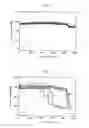
If an impurity is mixed in the active layer, since a nonradiative recombination center is formed causing problems, such as the lowering of emission intensity and the movement of the PN-junction (deviation from the design value), a semiconductor optical element that has favorable characteristics cannot be manufactured. FIG. 4 shows the results of a reliability test of a conventional semiconductor optical element having the structure shown in Table 1. Sudden death is observed at about 400 hours after starting the reliability test, and the structure cannot be the to have sufficient reliability.
SUMMARY OF THE INVENTIONThe present invention has been devised to solve the above-described problems, and an object of the present invention is to provide a semiconductor optical element that can prevent the mixing of impurities in the active layer, enhance power, and improve the reliability of operations.
According to one aspect of the present invention, a semiconductor optical element has a structure wherein an n-type GaAs buffer layer, an n-type AlGaInP clad layer, a first InGaAsP (including zero As content) guide layer without adding impurities, an InGaAsP (including zero In content) active layer, a second InGaAsP (including zero As content) guide layer without adding impurities, a p-type AlGaInP clad layer, a p-type band discontinuity reduction layer, and a p-type GaAs contact layer are sequentially laminated on an n-type GaAs substrate; wherein C or Mg is used as the p-type impurity for the p-type GaAs contact layer, the p-type band discontinuity reduction layer, and the p-type AlGaInP clad layer.
According the present invention, the mixing of impurities in the active layer can be prevented, power can be enhanced, and the reliability of operations can be improved.
Other and further objects, features and advantages of the invention will appear more fully from the following description.
BRIEF DESCRIPTION OF THE DRAWINGSFIG. 1 is a diagram showing the results of a reliability test for a semiconductor optical element according to the First Embodiment of the present invention;
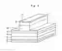
FIG. 2 is a sectional view showing a ridge waveguide type laser to which the semiconductor optical element of the present invention can be applied;
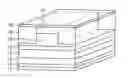
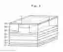
FIG. 3 is a sectional view showing a embedded type laser having a current confinement structure to which the semiconductor optical element of the present invention can be applied; and
FIG. 4 is a diagram showing the results of a reliability test for a conventional semiconductor optical element.
DETAILED DESCRIPTION OF THE PREFERRED EMBODIMENTS First EmbodimentTable 2 shows the impurity to be added, carrier concentration, and film thickness of each layer in a semiconductor optical element according to the First Embodiment of the present invention. Here, as an example, a laminated structure of a semiconductor optical element used in a power source that uses a GaAsP/InGaP-based material used for exciting a solid laser in an 808-nm band.
| TABLE 2 | |||
| Carrier | |||
| concentration | Film thickness | ||
| Layer name | Impurity | (1018/cm3) | (nm) |
| p-type GaAs contact | C | 30.0-50.0 | 100-500 |
| layer | |||
| p-type InGaP-BDR | Mg | 1.0-3.0 | 20-100 |
| layer | |||
| p-type AlGaInP clad | Mg | 1.0-2.0 | 500-1500 |
| layer | |||
| InGaAsP guide layer | — | — | 500-1500 |
| GaAsP active layer | — | — | 5-12 |
| InGaAsP guide layer | — | — | 500-1500 |
| n-type AlGaInP clad | Si | 0.5-1.5 | 500-1500 |
| layer | |||
| n-type GaAs buffer | Si | 0.5-1.5 | 200-700 |
| layer | |||
| n-type GaAs substrate | Si | 0.7-1.0 | — |
In the semiconductor optical element of Table 2, an n-type GaAs (or AlGaAs) buffer layer to which Si is added as an n-type impurity, an n-type AlGaInP clad layer to which Si is added, a InGaAsP guide layer without adding impurities, a GaAsP active layer without adding impurities, an InGaAsP guide layer without adding impurities, a p-type AlGaInP clad layer to which Mg is added as a p-type impurity, a p-type InGaP-BDR (band discontinuity reduction) layer to which Mg is added, and a GaAs contact layer to which C is added are sequentially laminated on an n-type GaAs substrate.
As a method for lamination, for example, a crystal growing technique, such as an MOCVD method, is used. In the case of MOCVD growth, the growing temperature is 720° C., the growing pressure is, for example, 100 mbar; and as the raw materials for forming each layer, for example, trimethyl indium (TMI), trimethyl gallium (TMG), trimethyl aluminum (TMA), phosphine (PH3), arsine (ASH3), silane (SiH4), diethyl zinc (DEZn) or the like is used. The flow rates of these material gases are controlled using a mass flow controller or the like to obtain a desired composition.
In the growth of the p-type GaAs contact layer, the growing temperature is, for example, 540° C., and the V/III ratio (flow rate of AsH3 to TMG) is about 1. Normally, the growing temperature for growing a GaAs layer is about 600 to 750° C., and the V/III ratio is several tens to several hundreds. By growing it under the above-described growing conditions, C liberated from methyl groups originally contained in TMG is incorporated without introducing a special material for adding the impurity. Such an intrinsic impurity introducing method can be used, or carbon tetrachloride (CCl4), carbon tetrabromide (CBr4) or the like can also be used.
In the First Embodiment, as described above, the p-type impurity to be added to the p-type GaAs contact layer is C, and the p-type impurity to be added to the p-type InGaP-BDR layer and the p-type AlGaInP clad layer is Mg. Mg and C have smaller diffusion coefficients than Zn. Theoretically, no mutual diffusion occurs between C in the p-type GaAs contact layer and Mg in the p-type AlGaInP clad layer. Therefore, the diffusion of impurities into the active layer, which can be observed when Zn is used, can be suppressed.
From this fact, the C concentration in the p-type GaAs contact layer, and the Mg concentration in the p-type InGaP-BDR layer, and the p-type AlGaInP clad layer in the vicinity of the active layer can be elevated compared with the conventional case using Zn.
According to the First Embodiment, therefore, since the diffusion of p-type impurities into the GaAsP active layer can be suppressed while maintaining the carrier concentration in the p-type GaAs contact layer at 4.0×10¹⁹/cm3, and the hole concentration in the p-type AlGaInP clad layer at 2×10¹⁸/cm3, a high-power high-efficiency semiconductor optical element can be realized while maintaining high reliability.
FIG. 1 shows the results of a reliability test of a semiconductor optical element having the structure shown in Table 2. No sudden death occurred at 1000 hours after starting the reliability test exhibiting sufficient reliability.
When the p-type impurity added to the p-type InGaP-BDR layer and the p-type AlGaInP clad layer is Mg, the film formation temperature of the p-type InGaP-BDR layer and the p-type AlGaInP clad layer can be higher than the case wherein all the p-type impurity is C, and the crystallinity of the p-type InGaP-BDR layer and the p-type AlGaInP clad layer can be elevated; therefore, a high-efficiency semiconductor optical element can be obtained.
The above-described semiconductor optical element can be applied to either a ridge waveguide structure laser shown in FIG. 2, or a buried laser having a current confinement structure shown in FIG. 3. In the laser shown in FIG. 2, an n-type electrode 11, an n-type GaAs substrate 12, an n-type GaAs buffer layer 13, an n-type clad layer 14, a GaAsP/InGaP quantum well structure 15, a p-type clad layer 16, a p-type contact layer 17, and a p-type electrode 18 are laminated sequentially from the bottom. In the laser shown in FIG. 3, n-type current block layers 19 are further provided.
In the First Embodiment, although the case using one GaAsP active layer was described, it is not intended to limit the number of active layers, but the same effect can be obtained when tow or more active layers are used. The thickness of each layer shown in Table 2 is not also limited.
Second EmbodimentTable 3 shows the impurity to be added, carrier concentration, and film thickness of each layer in a semiconductor optical element according to the Second Embodiment of the present invention.
| TABLE 3 | |||
| Carrier | |||
| concentration | Film thickness | ||
| Layer name | Impurity | (1018/cm3) | (nm) |
| p-type GaAs contact | C | 30.0-50.0 | 100-500 |
| layer | |||
| p-type InGaP-BDR | C | 1.0-3.0 | 20-100 |
| layer | |||
| p-type AlGaInP clad | C | 1.0-2.0 | 500-1500 |
| layer | |||
| InGaAsP guide layer | — | — | 500-1500 |
| GaAsP active layer | — | — | 5-12 |
| InGaAsP guide layer | — | — | 500-1500 |
| n-type AlGaInP clad | Si | 0.5-1.5 | 500-1500 |
| layer | |||
| n-type GaAs buffer | Si | 0.5-1.5 | 200-700 |
| layer | |||
| n-type GaAs substrate | Si | 0.7-1.0 | — |
In the Second Embodiment, the p-type impurity added to the p-type GaAs contact layer, the p-type InGaP-BDR layer, and the p-type AlGaInP clad layer is C. Other constitutions are the same as in the First Embodiment. Thereby, the mixing of impurities in the active layers can be prevented, power can be enhanced, and the reliability of operations can be improved.
Since no p-type dopant materials are required by using C as the p-type impurity to be added to all of the p-type GaAs contact layer, the p-type InGaP-BDR layer, and the p-type AlGaInP clad layer, the fabricating costs can be reduced.
In addition, the fabricating method is substantially the same as in the First Embodiment. However, carbon tetrachloride (CCl4) or carbon tetrabromide (CBr4) must be used for adding C to the AlGaInP layer, and the intrinsic impurity introducing method as described in the First Embodiment cannot be used.
Third EmbodimentTable 4 shows the impurity to be added, carrier concentration, and film thickness of each layer in a semiconductor optical element according to the Third Embodiment of the present invention.
| TABLE 4 | |||
| Carrier | |||
| concentration | Film thickness | ||
| Layer name | Impurity | (1018/cm3) | (nm) |
| p-type GaAs contact | Mg | 30.0-50.0 | 100-500 |
| layer | |||
| p-type InGaP-BDR | Mg | 1.0-3.0 | 20-100 |
| layer | |||
| p-type AlGaInP clad | Mg | 1.0-2.0 | 500-1500 |
| layer | |||
| InGaAsP guide layer | — | — | 500-1500 |
| GaAsP active layer | — | — | 5-12 |
| InGaAsP guide layer | — | — | 500-1500 |
| n-type AlGaInP clad | Si | 0.5-1.5 | 500-1500 |
| layer | |||
| n-type GaAs buffer | Si | 0.5-1.5 | 200-700 |
| layer | |||
| n-type GaAs substrate | Si | 0.7-1.0 | — |
In the Third Embodiment, the p-type impurity added to the p-type GaAs contact layer, the p-type InGaP-BDR layer, and the p-type AlGaInP clad layer is Mg. Other constitutions are the same as in the First Embodiment. The fabricating method is the same as the method for adding Mg described in the First Embodiment. Thereby, as in the First Embodiment the mixing of impurities in the active layers can be prevented, power can be enhanced, and the reliability of operations can be improved.
In addition, Since the growing temperature can be set higher than the temperature at which C doping is performed by using Mg as the p-type impurity to be added to all of the p-type GaAs contact layer, the p-type InGaP-BDR layer, and the p-type AlGaInP clad layer, the crystallinity of the semiconductor optical element can be elevated.
Fourth EmbodimentThe semiconductor optical element according to the Fourth Embodiment of the present invention is a semiconductor optical element wherein the GaAsP active layer described in Tables 2 to 4 is substituted by an InGaAsP active layer. However, in the InGaAsP composition, the PL light-emitting wavelength of the InGaAsP/InGaP quantum well structure is 790 to 810 nm. Other element structures, the combination of the p-type impurities to be added, and the fabricating methods are the same as in the first to Third Embodiments. Thereby, the effect same as in the first to Third Embodiments can be obtained.
Obviously many modifications and variations of the present invention are possible in the light of the above teachings. It is therefore to be understood that within the scope of the appended claims the invention may be practiced otherwise than as specifically described.
The entire disclosure of a Japanese Patent Application No. 2005-059595, filed on Mar. 3, 2005 including specification, claims, drawings and summary, on which the Convention priority of the present application is based, are incorporated herein by reference in its entirety.
Claims
1. A semiconductor optical element comprising an n-type GaAs buffer layer, an n-type AlGaInP cladding layer, a first InGaAsP (including zero As content) guide layer without added dopant impurities, an InGaAsP (including zero In content) active layer, a second InGaAsP (including zero As content) guide layer without added dopant impurities, a p-type AlGaInP cladding layer, a p-type band discontinuity reduction layer, and a p-type GaAs contact layer, sequentially laminated, on an n-type GaAs substrate, wherein one of C and Mg is the dopant impurity in the p-type GaAs contact layer, the p-type band discontinuity reduction layer, and the p-type AlGaInP cladding layer.
2. The semiconductor optical element according to claim 1, wherein C is the dopant impurity for the p-type GaAs contact layer, and Mg is the dopant impurity in the p-type band discontinuity reduction layer and the p-type AlGaInP cladding layer.
3. The semiconductor optical element according to claim 1, wherein C is the dopant impurity in the p-type GaAs contact layer, the p-type band discontinuity reduction layer, and the p-type AlGaInP cladding layer.
4. The semiconductor optical element according to claim 1, wherein Mg is the dopant impurity in the p-type GaAs contact layer, the p-type band discontinuity reduction layer, and the p-type AlGaInP cladding layer.
Images & Drawings included:
Sources:
- United States Patent and Trademark Office - verify current appl. status at the USPTO↗
Similar patent applications:
- » 20220294188
Semiconductor optical element, semiconductor optical element forming structure, and method of manufacturing semiconductor optical element using the same - » 20200403381
Semiconductor optical element, semiconductor optical element forming structure, and method for manufacturing semiconductor optical element using the same - » 20140055842
Semiconductor optical element, integrated semiconductor optical element, and semiconductor optical element module - » 20210075194
Semiconductor optical element, semiconductor optical integrated element, and method for manufacturing semiconductor optical element - » 20150180203
Semiconductor optical element, semiconductor laser element, and method for manufacturing semiconductor optical element and semiconductor laser element, and method for manufacturing semiconductor laser module and semiconductor element - » 20150349495
Semiconductor optical element, semiconductor laser element, and method for manufacturing semiconductor optical element and semiconductor laser element, and method for manufacturing semiconductor laser module and semiconductor element - » 20240363795
SEMICONDUCTOR OPTICAL ELEMENT, MEASUREMENT DEVICE AND LIGHT SOURCE DEVICE USING SEMICONDUCTOR OPTICAL ELEMENT, AND METHOD FOR MANUFACTURING SEMICONDUCTOR OPTICAL ELEMENT - » 20140235806
Curable silicone composition for sealing an optical semiconductor element, method of producing a resin-sealed optical semiconductor element, and resin-sealed optical semiconductor element - » 20240405514
SEMICONDUCTOR OPTICAL ELEMENT, MEASUREMENT DEVICE AND LIGHT SOURCE DEVICE USING SEMICONDUCTOR OPTICAL ELEMENT, AND METHOD OF MANUFACTURING SEMICONDUCTOR OPTICAL ELEMENT - » 20100150579
Semiconductor optical element, semiconductor laser using the semiconductor optical element, and optical transponder using the semiconductor laser
Recent applications in this class:
- » 20250253621 2025-08-07
SEMICONDUCTOR OPTICAL DEVICE AND METHOD OF MANUFACTURING SEMICONDUCTOR OPTICAL DEVICE - » 20250149861 2025-05-08
OXIDE-CONFINED SEMICONDUCTOR LASER HAVING HIGH ALUMINUM CONTENT AND METHOD OF FABRICATING THE SAME - » 20250096532 2025-03-20
OPTICAL SEMICONDUCTOR DEVICE - » 20250038482 2025-01-30
SEMICONDUCTOR COMPONENT - » 20250023330 2025-01-16
Double Waveguide Structure For Edge-Emitting Semiconductor Laser And Method Of Forming The Same - » 20240380180 2024-11-14
SEMICONDUCTOR LASER ELEMENT AND METHOD FOR MANUFACTURING THE SAME - » 20240322526 2024-09-26
High-Power Edge-Emitting Laser Device and Manufacturing Method Thereof - » 20240250505 2024-07-25
NITRIDE SEMICONDUCTOR LIGHT-EMITTING ELEMENT - » 20240186767 2024-06-06
METHOD OF MANUFACTURING SEMICONDUCTOR OPTICAL DEVICE - » 20240170922 2024-05-23
SEMICONDUCTOR LASER, ELECTRONIC APPARATUS, AND METHOD FOR MANUFACTURING SEMICONDUCTOR LASER
Recent applications for this Assignee:
- » 20190149764 2019-05-16
Randomly accessible visual information recording medium and recording method, and reproducing device and reproducing method - » 20180054591 2018-02-22
Randomly accessible visual information recording medium and recording method, and reproducing device and reproducing method - » 20160006976 2016-01-07
Randomly accessible visual information recording medium and recording method, and reproducing device and reproducing method - » 20150179217 2015-06-25
Randomly accessible visual information recording medium and recording method, and reproducing device and reproducing method - » 20150147051 2015-05-28
Randomly accessible visual information recording medium and recording method, and reproducing device and reproducing method - » 20150139628 2015-05-21
Randomly accessible visual information recording medium and recording method, and reproducing device and reproducing method - » 20150139626 2015-05-21
Randomly accessible visual information recording medium and recording method, and reproducing device and reproducing method - » 20150139625 2015-05-21
Randomly accessible visual information recording medium and recording method, and reproducing device and reproducing method - » 20150139624 2015-05-21
Randomly accessible visual information recording medium and recording method, and reproducing device and reproducing method - » 20150139623 2015-05-21
Randomly accessible visual information recording medium and recording method, and reproducing device and reproducing method