Semiconductor laser diode
US20060222037A1
2006-10-05
11/294,555
2005-12-06
Abstract:
A semiconductor laser diode includes a semiconductor cladding layer of a first conductivity type, an active layer on the semiconductor cladding layer of the first conductivity type, a semiconductor cladding layer of a second conductivity type on the active layer, an insulating film on the semiconductor cladding layer of the second conductivity type, a metal electrode electrically connected to the semiconductor cladding layer of the second conductivity type, and an electric circuit element on the insulating film.
Assignee:
- MITSUBISHI DENKI KABUSHIKI KAISHA 1,758 🇯🇵 Tokyo, Japan
Interested in similar patents?
Get notified when new applications in this technology area are published.
Classification:
H01S5/0261 » CPC main
Semiconductor lasers; Structural details or components not essential to laser action; Monolithically integrated components, e.g. waveguides, monitoring photo-detectors, drivers Non-optical elements, e.g. laser driver components, heaters
H01S5/04254 » CPC further
Semiconductor lasers; Processes or apparatus for excitation, e.g. pumping, e.g. by electron beams; Electrical excitation ; Circuits therefor; Electrodes, e.g. characterised by the structure characterised by the shape
H01S5/227 » CPC further
Semiconductor lasers; Structure or shape of the semiconductor body to guide the optical wave ; Confining structures perpendicular to the optical axis, e.g. index or gain guiding, stripe geometry, broad area lasers, gain tailoring, transverse or lateral reflectors, special cladding structures, MQW barrier reflection layers having a ridge or stripe structure Buried mesa structure ; Striped active layer
H01S5/0427 » CPC further
Semiconductor lasers; Processes or apparatus for excitation, e.g. pumping, e.g. by electron beams; Electrical excitation ; Circuits therefor for applying modulation to the laser
H01S3/097 IPC
Lasers, i.e. devices using stimulated emission of electromagnetic radiation in the infrared, visible or ultraviolet wave range; Processes or apparatus for excitation, e.g. pumping by gas discharge of a gas laser
Description
BACKGROUND OF THE INVENTION1. Field of the Invention
The present invention relates to a semiconductor laser diode that converts an electric input signal into light and outputs the light.
2. Background Art
A semiconductor laser diode is a device that converts an electric input signal into light and outputs the light. Conventionally, an electric circuit element has been disposed outside the semiconductor laser diode in order to optimize the input signal depending on purposes or uses. For example, a terminal resistor is connected in series to a semiconductor laser diode. Although there is an optical modulator to which a terminal resistor is connected in parallel (e.g., refer to Japanese Patent Laid-Open No. 2004-219949), both means and effects differ from those in the case of a semiconductor laser diode.
However, since an electric circuit element is disposed outside, it was difficult downsize the total constitution including the electric circuit element. In addition, there was a problem that the frequency responding characteristics of input signals were deteriorated because of parasitic impedance produced by the connection of the semiconductor laser diode to the external electric circuit element.
SUMMARY OF THE INVENTIONThe present invention has been made to solve foregoing problems, and it is an object of the present invention to provide a semiconductor laser diode that can downsize the total constitution including an electric circuit element, and can reduce parasitic impedance produced by the connection to an electric circuit element to prevent the deterioration of frequency responding characteristics of input signals.
According to one aspect of the present invention, a semiconductor laser diode comprises a semiconductor clad layer of a first conductivity type, an active layer formed on the semiconductor clad layer of a first conductivity type, a semiconductor clad layer of a second conductivity type formed on the active layer, an insulation film formed on the semiconductor clad layer of a second conductivity type, a metal electrode electrically connected to the semiconductor clad layer of a second conductivity type, and an electric circuit element formed on the insulation film.
Other and further objects, features and advantages of the invention will appear more fully from the following description.
According to the present invention, a semiconductor laser diode that can downsize the total constitution including an electric circuit element, and can reduce parasitic impedance produced by the connection to an electric circuit element to prevent the deterioration of frequency responding-characteristics of input signals.
BRIEF DESCRIPTION OF THE DRAWINGSFIG. 1 is a perspective view showing a semiconductor laser diode according to the first embodiment of the present invention.
FIG. 2 is a perspective view showing a semiconductor laser diode according to the second embodiment of the present invention.
FIG. 3 is a perspective view showing a semiconductor laser diode according to the third embodiment of the present invention.
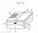
FIG. 4 is a perspective view showing a semiconductor laser diode according to the fourth embodiment of the present invention.
DETAILED DESCRIPTION OF THE PREFERRED EMBODIMENTSFirst Embodiment
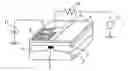
FIG. 1 is a perspective view showing a semiconductor laser diode according to the first embodiment of the present invention.
On a semiconductor clad layer of a first conductivity type 1, an active layer 2 is formed, and a semiconductor clad layer of a second conductivity type 3 is formed thereon. Current block layers 4 are formed on the both sides of the active layer 2, and an insulation film 5 is formed on the semiconductor clad layer of the second conductivity type 3. A metal electrode 6 is formed so as to electrically connect to the semiconductor clad layer of the second conductivity type 3.
Further, in the semiconductor laser diode according to the first embodiment, a resistor 7 is formed on the insulation film 5 as an electric circuit element. The resistor 7 can be formed by the vapor deposition of a thin film. The resistor 7 is electrically connected to the metal electrode 6.
By thus incorporating the resistor 7, no resistors are required to install outside so as to prevent the deterioration of frequency responding characteristics of input signals produced by the mismatch of impedance between the semiconductor laser diode and the drive circuit; therefore, the total constitution including the resistor 7 can be downsized. Further, parasitic impedance produced by the connection to the resistor 7 can be reduced to prevent the deterioration of frequency responding characteristics of input signals. Since optional input impedance can be obtained by using resistors of different resistance, the impedance can be easily matched with the drive circuit.
Second Embodiment
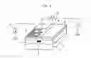
FIG. 2 is a perspective view showing a semiconductor laser diode according to the second embodiment of the present invention. In the semiconductor laser diode according to the second embodiment, an inductor 9 is formed on an insulation film 5 as an electric circuit element. The inductor 9 is electrically connected to the metal electrode 6, and is formed by a spiral pattern of the same composition as the metal electrode 6. Other constitutions are the same as those of the first embodiment.
By thus incorporating the inductor 9, no installation of an inductor that constitute a bias circuit of direct current component for preventing increase in power consumption of the drive circuit and the heat generation of the resistance portion caused by flowing the direct current components in an impedance matching resistor for isolating the direct current component and high frequency (frequency modulation) component of input signals and preventing the deterioration of frequency responding characteristics; therefore, the total constitution including the inductor 9 can be downsized as in the case of the first embodiment 1. Further, parasitic impedance produced by the connection to the inductor 9 element can be reduced to prevent the deterioration of frequency responding characteristics of input signals.
A metal electrode 6 is connected to a pulse generator 11 through a matching resistor 10, and a direct current source 12 is connected to the inductor 9. Thereby the direct current component of input signals can be supplied through the inductor, and the high frequency component of input signals can be supplied without involving the inductor.
Third embodiment
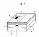
FIG. 3 is a perspective view showing a semiconductor laser diode according to the third embodiment of the present invention. In the first embodiment, only a resistor is formed as an electric circuit element; and in the second embodiment, only an inductor is formed as an electric circuit element. Whereas in the semiconductor laser diode according to the third embodiment, a resistor 7 and an inductor 9 are formed as electric circuit elements on the insulation film 5. Other constitutions are the same as those of the first embodiment. Thereby, the effects of both the first embodiment and the second embodiment can be obtained.
Fourth Embodiment
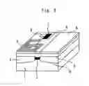
FIG. 4 is a perspective view showing a semiconductor laser diode according to the fourth embodiment of the present invention. In the semiconductor laser diode according to the fourth embodiment, a capacitor 13 is formed on an insulation film 5 as an electric circuit element. The capacitor 13 is electrically connected to the metal electrode 6. The capacitor 13 is composed of a pattern having the same composition of the metal electrode 6 formed in the insulation film 5, a semiconductor clad layer of the second conductivity type 3 having a different potential, and an insulation film 5 interposed between them. Other constitutions are the same as those of the first embodiment.
By thus incorporating the capacitor 13, as in the first embodiment, the total constitution including the capacitor 13 can be downsized, and parasitic impedance produced by the connection to the capacitor 13 can be reduced to prevent the deterioration of frequency responding characteristics of input signals.
Further, a low-pass filter can be composed of the capacitance component of the capacitor and the inductance component of the wire for connecting to the drive circuit, and by truncating unnecessary harmonic components of the input signals, high-purity signals can be transmitted.
Obviously many modifications and variations of the present invention are possible in the light of the above teachings. It is therefore to be understood that within the scope of the appended claims the invention may be practiced otherwise than as specifically described.
The entire disclosure of a Japanese Patent Application No. 2005-107997, filed on Apr. 4, 2005 including specification, claims, drawings and summary, on which the Convention priority of the present application is based, are incorporated herein by reference in its entirety.
Claims
1. A semiconductor laser diode comprising:
a semiconductor cladding layer of a first conductivity type;
an active layer formed on the semiconductor cladding layer of the first conductivity type;
a semiconductor cladding layer of a second conductivity type formed on the active layer;
an insulating film on the semiconductor cladding layer of the second conductivity type;
a metal electrode electrically connected to the semiconductor cladding layer of the second conductivity type; and
an electric circuit element on the insulating film.
2. The semiconductor laser diode according to claim 1, wherein the electric circuit element is electrically connected to the metal electrode.
3. The semiconductor laser diode according to claim 1, wherein the electric circuit element is a resistor.
4. The semiconductor laser diode according to claim 2, wherein the electric circuit element is a resistor.
5. The semiconductor laser diode according to claim 1, wherein the electric circuit element is an inductor.
6. The semiconductor laser diode according to claim 2, wherein the electric circuit element is an inductor.
7. The semiconductor laser diode according to claim 1, wherein the electric circuit element is a capacitor.
8. The semiconductor laser diode according to claim 2, wherein the electric circuit element is a capacitor.
Images & Drawings included:
Sources:
- United States Patent and Trademark Office - verify current appl. status at the USPTO↗
Similar patent applications:
- » 20160315446
Semiconductor laser diode, method for producing a semiconductor laser diode and semiconductor laser diode arrangement - » 20210313760
METHOD FOR MANUFACTURING SEMICONDUCTOR LASER DIODE AND SEMICONDUCTOR LASER DIODE - » 20150244147
METHOD FOR PRODUCING A SEMICONDUCTOR LASER DIODE, AND SEMICONDUCTOR LASER DIODE - » 20070110113
Semiconductor laser diode and semiconductor laser diode assembly containing the same - » 20080219309
Method of fabricating semiconductor laser diode apparatus and semiconductor laser diode apparatus - » 20250015561
METHOD FOR PRODUCING A MULTIPLICITY OF VERTICALLY EMITTING SEMICONDUCTOR LASER DIODES AND VERTICALLY EMITTING SEMICONDUCTOR LASER DIODE - » 20210126424
SEMICONDUCTOR LASER DIODE AND METHOD FOR PRODUCING SEMICONDUCTOR LASER DIODE - » 20200112142
Semiconductor laser diode and method for manufacturing a semiconductor laser diode - » 20060071218
Semiconductior multilayer structurehaving inhomogeneous quantum dots, light-emitting diode using same, semiconductor laser diode, semiconductor optical amplifier, and method for manufacturing them - » 20180152002
Semiconductor laser diode and method for producing a semiconductor laser diode
Recent applications in this class:
- » 20250174964 2025-05-29
MULTI-CHANNEL COMMON-CATHODE PULSED LASER DIODE DRIVER - » 20250158356 2025-05-15
Optical Transmitter - » 20250023324 2025-01-16
Pulsed laser diode driver - » 20240204478 2024-06-20
DRIVER CIRCUIT, CORRESPONDING LASER-DRIVING DEVICE, LASER LIGHTING MODULE, LIDAR APPARATUS AND METHODS OF OPERATION - » 20240154385 2024-05-09
Semiconductor laser drive device and method of manufacturing the same - » 20230361527 2023-11-09
LASER SYSTEM - » 20230275397 2023-08-31
Pulsed laser diode driver - » 20230111084 2023-04-13
METHODS AND DEVICES FOR AN ELECTRICALLY EFFICIENT GREEN LASER DIODE DRIVE SYSTEM WITH BOOST SERVO - » 20220407289 2022-12-22
OPTICAL ASSEMBLY WITH A VERTICAL CAVITY SURFACE EMITTING LASER DEVICE DISPOSED ON AN INTEGRATED CIRCUIT DRIVER CHIP - » 20220376463 2022-11-24
TUNABLE LASER WITH CHANNEL SELECTOR
Recent applications for this Assignee:
- » 20190149764 2019-05-16
Randomly accessible visual information recording medium and recording method, and reproducing device and reproducing method - » 20180054591 2018-02-22
Randomly accessible visual information recording medium and recording method, and reproducing device and reproducing method - » 20160006976 2016-01-07
Randomly accessible visual information recording medium and recording method, and reproducing device and reproducing method - » 20150179217 2015-06-25
Randomly accessible visual information recording medium and recording method, and reproducing device and reproducing method - » 20150147051 2015-05-28
Randomly accessible visual information recording medium and recording method, and reproducing device and reproducing method - » 20150139628 2015-05-21
Randomly accessible visual information recording medium and recording method, and reproducing device and reproducing method - » 20150139626 2015-05-21
Randomly accessible visual information recording medium and recording method, and reproducing device and reproducing method - » 20150139625 2015-05-21
Randomly accessible visual information recording medium and recording method, and reproducing device and reproducing method - » 20150139624 2015-05-21
Randomly accessible visual information recording medium and recording method, and reproducing device and reproducing method - » 20150139623 2015-05-21
Randomly accessible visual information recording medium and recording method, and reproducing device and reproducing method