Control circuit for command signals of clock generator
US20060232324A1
2006-10-19
11/306,922
2006-01-17
✅ Patent granted
US 7,298,186 B2
2007-11-20
-
-
Jeffrey Zweizig
2026-06-26
Abstract:
A control circuit for command signals of a clock generator includes a power supply end, an output end, a control end, a diode, a first resistor and a second resistor. The first resistor, the diode, and the second resistor are connected in series between the power supply end and the ground. The diode has an anode connected to the first resistor and a cathode connected to the second resistor. The control end is connected to a node between the diode and the second resistor; the output end is connected to a node between the diode and the first resistor. The output end outputs the command signals to the clock generator.
Inventors:
- YONG-ZHAO HUANG 65 🇨🇳 Shenzhen, China
- Yun Li 15 🇨🇳 Shenzhen, China
- Yong-Xing You 26 🇨🇳 Shenzhen, China
- Wu Jiang 14 🇨🇳 Shenzhen, China
Assignee:
- Hong Fu Jin Precision Industry (Shen Zhen) Co., Ltd. 33 🇨🇳 Shenzhen, Guangdong Province, China
- Hon Hai Precision Industry Co., Ltd. 1 🇹🇼 Tu-Cheng, Teipei Hsien, Taiwan
Interested in similar patents?
Get notified when new applications in this technology area are published.
Classification:
G11C7/22 » CPC main
Arrangements for writing information into, or reading information out from, a digital store Read-write [R-W] timing or clocking circuits; Read-write [R-W] control signal generators or management
G11C7/222 » CPC further
Arrangements for writing information into, or reading information out from, a digital store; Read-write [R-W] timing or clocking circuits; Read-write [R-W] control signal generators or management Clock generating, synchronizing or distributing circuits within memory device
H03K17/74 » CPC further
Electronic switching or gating, i.e. not by contact-making and –breaking characterised by the components used by the use, as active elements, of diodes
G11C5/14 IPC
Details of stores covered by group Power supply arrangements, e.g. power down, chip selection or deselection, layout of wirings or power grids, or multiple supply levels
H03L7/00 IPC
Automatic control of frequency or phase; Synchronisation
Description
DESCRIPTION1. Field of the Invention
The present invention relates in general to a control circuit of command signals, and more particular to a control circuit of command signals of a clock generator.
2. Description of Related Art
A clock generator mounted on a motherboard of a computer is used to determine the CPU, PCI, and system bus speeds. The clock generator is controlled by command signals from a control circuit. If all of the voltages at the planar connector from the power supply are within a predetermined tolerance level, i.e. within specification, the power good (PG) signal goes high thereby causing the clock generator to generate clock signals to a computer system.
FIG. 3 illustrates a conventional control circuit for command signals of a clock generator. The control circuit includes two transistors Q1 and Q2. A base of the transistor Q1 is connected via a resistor R3 to a control end Vccp, a collector of the transistor Q1 is coupled to a power supply end Vdc via a resistor R1, the collector of the transistor Q1 is also coupled to a base of the transistor Q2. A collector of the transistor Q2 is connected to the power supply end Vdc via a resistor R2. Emitters of the two transistors Q1 and Q2 are grounded. The collector of the transistor Q2 is connected to an output end VTT_PWRGD via a resistor R4. The output end VTT_PWRGD outputs the command signal PG to a clock generator. The voltage of the power supply end Vdc is provided by the motherboard and the value is 3.3V. When the voltage of the control end Vccp is at a high level, the transistor Q1 is turned on, the transistor Q2 is turned off, the voltage at the output end VTT_PWRGD is at a high level to enable the clock generator to generate clock signals; when the voltage of the control end Vccp is at a low level, the transistor Q1 is turned off, the transistor Q2 is turned on, the voltage at the output end VTT_PWRGD is at a low level, the clock generator does not generate clock signals. However, employing the two transistors to control the command signals of the clock generator increases the cost of the manufacture of the motherboard.
What is needed, therefore, is a control circuit for command signal of clock generator which not only accomplishes the same efficiency of the prior art, but also can be mass produced at a reasonable cost.
SUMMARY OF INVENTIONAn exemplary control circuit for command signals of a clock generator includes a power supply end, an output end, a control end, a diode, a first resistor and a second resistor. The first resistor, the diode, and the second resistor are connected in series between the power supply end and the ground. The diode has an anode connected to the first resistor and a cathode connected to the second resistor. The control end is connected to a node between the diode and the second resistor; the output end is connected to a node between the diode and the first resistor. The output end outputs the command signals to the clock generator.
It is of advantage that employing a diode as a switch to replace the two transistors of the prior art can be mass produced at a reasonable cost.
Other advantages and novel features will become more apparent from the following detailed description of preferred embodiments when taken in conjunction with the accompanying drawings, in which:
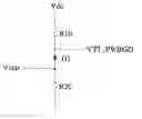
BRIEF DESCRIPTION OF DRAWINGSFIG. 1 is a circuit diagram of a control circuit for command signals in accordance with a preferred embodiment of the present invention;
FIG. 2 is a comparative graph showing signal waveforms obtained using the circuits of FIG. 1 and FIG. 3; and
FIG. 3 is a circuit diagram of a conventional control circuit for command signals of a clock generator.
DETAILED DESCRIPTIONReferring to FIG. 1, a control circuit for command signals of a clock generator includes a diode D1, a first resistor R10, a second resistor R20, a control end Vccp, a power supply end Vdc, and an output end VTT_PWRGD. The first resistor R1, the diode D1, and the second resistor R2 are connected in series between the power supply end Vdc and the ground. An anode of the diode D1 is connected to the first resistor R1, and a cathode of the diode D1 is connected to the second resistor R20. The control end Vccp is connected at a node between the diode D1 and the second resistor R20. The output end VTT_PWRGD is connected to a node between the first resistor R10 and the diode D1. A voltage of the power supply end Vdc is 3.3V.
When the voltage of the control end Vccp is at a high level, the diode D1 is turned off, the voltage at the output end VTT_PWRGD is at a high level to enable the clock generator to generate clock signals; when the voltage of the control end Vccp is at a low level, the diode D1 is turned on, the voltage at the output end VTT_PWRGD is at a low level, the clock generator does not generate clock signals.
FIG. 2 is a comparative graph showing signal waveforms obtained using the circuits of FIG. 1 and FIG. 3. Line 1 denotes the signal waveform obtained using the circuit of FIG. 3, and line 2 denotes the signal waveform obtained using the circuit of FIG. 1. As shown in FIG. 2, employing the control circuit for command signals of the clock generator of the present invention accomplishes the same efficiency of the FIG. 3. The embodiment of the invention only uses a diode D1 as a switch to control the voltage at the output end VTT_PWRGD to save the cost of the manufacture of the motherboard.
It is to be understood, however, that even though numerous characteristics and advantages of the present embodiment has been set forth in the foregoing description, together with details of the structure and function of the invention, the disclosure is illustrative only, and changes may be made in detail, especially in matters of shape, size, and arrangement of parts within the principles of the invention to the full extent indicated by the broad general meaning of the terms in which the appended claims are expressed.
Claims
What is claimed is:1. A control circuit for command signals of a clock generator comprising a power supply end, an output end, and a control end; a diode, a first resistor and a second resistor connected in series between the power supply end and the ground, the control end connected to a node between the diode and the second resistor, the output end connected to a node between the diode and the first resistor, wherein the output end outputs the command signals to the clock generator.
2. The control circuit as claimed in claim 1, wherein the diode has an anode connected to the first resistor and a cathode connected to the second resistor.
3. The control circuit as claimed in claim 2, wherein the power supply end has a voltage of 3.3V.
4. A control circuit for command signals of a clock generator comprising a power supply end, an output end, a control end, a first resistor, a second resistor, and a switch, the first resistor, the second resistor and the switch connected in series between the power supply end and the ground, the control end connected to a node between the diode and the second resistor, the output end connected to a node between the diode and the first resistor, wherein the output end outputs the command signals to the clock generator, when the voltage at the control end is at a high level, the switch is turned off to output a high voltage at the voltage output end, when the voltage at the control end is at a low level, the switch turned on to output a low voltage at the voltage output end.
Images & Drawings included:


Sources:
- United States Patent and Trademark Office - verify current appl. status at the USPTO↗
Similar patent applications:
Recent applications in this class:
- » 20250226015 2025-07-10
On-Die Termination of Address and Command Signals - » 20250104749 2025-03-27
METHOD OF CALIBRATING IMPEDANCE OF MEMORY DEVICE AND IMPEDANCE CALIBRATION CIRCUIT PERFORMING THE SAME - » 20250087257 2025-03-13
CIRCUIT MODULE WITH IMPROVED TIMING CONTROL - » 20250037747 2025-01-30
APPARATUSES AND METHODS FOR PERFORMING LOGICAL OPERATIONS USING SENSING CIRCUITRY - » 20250037746 2025-01-30
On-die termination of address and command signals - » 20240428834 2024-12-26
STOP READ GO SETTINGS FOR LOW SUSPEND LATENCY APPLICATIONS - » 20240363153 2024-10-31
SIGNAL RETIMING WITHIN MEMORY SYSTEMS - » 20240355373 2024-10-24
METHOD AND DEVICE FOR ADJUSTING PHASE OF BIDIRECTIONAL DATA STROBE (DQS) SIGNAL - » 20240339139 2024-10-10
SEMICONDUCTOR MEMORY DEVICE INCLUDING MEMORY STRING AND PLURALITY OF SELECT TRANSITSTORS AND METHOD INCLUDING A WRITE OPERATION - » 20240274172 2024-08-15
MEMORY PACKAGE, STORAGE DEVICE INCLUDING MEMORY PACKAGE, AND STORAGE DEVICE OPERATING METHOD
Recent applications for this Assignee:
- » 20110114805 2011-05-19
Stand for electronic device - » 20110049139 2011-03-03
Device housing - » 20100165591 2010-07-01
Electronic device enclosure - » 20100120327 2010-05-13
Simulated eye - » 20100070792 2010-03-18
System and method for testing overclocking capability of CPU - » 20090251138 2009-10-08
Metal detector - » 20090103912 2009-04-23
Camera with external flash unit - » 20080239652 2008-10-02
Computer enclosure with drive bracket - » 20080141496 2008-06-19
Latch mechanism for slide rail assembly - » 20080074175 2008-03-27
Leakage current prevention circuit