One time programmable memory cell
US20060249791A1
2006-11-09
11/122,848
2005-05-05
✅ Patent granted
US 7,256,446 B2
2007-08-14
-
-
Douglas M. Menz
2025-05-26
Abstract:
This invention discloses a one-time programmable (OTP) memory cell. The OTP memory cell includes a dielectric layer disposed between two conductive polysilicon segments wherein the dielectric layer is ready to change from a non-conductive state to a conductive state through an induced voltage breakdown. In a preferred embodiment, one of the conductive polysilicon segments further includes an etch undercut configuration for conveniently inducing the voltage breakdown in the dielectric layer. In a preferred embodiment, the dielectric layer is further formed as sidewalls covering the edges and corners of a first polysilicon segments to conveniently induce a voltage breakdown in the dielectric layer by the edge and corner electrical field effects.
Inventors:
- SUNG-SHAN TAI 47 🇺🇸 San Jose, CA, United States
- Yongzhong Hu 19 🇺🇸 Cupertino, CA, United States
Assignee:
- Alpha and Omega Semiconductor, Ltd. 3 🇺🇸 Sunnyvale, CA, United States
Interested in similar patents?
Get notified when new applications in this technology area are published.
Classification:
G11C17/16 » CPC main
Read-only memories programmable only once; Semi-permanent stores, e.g. manually-replaceable information cards in which contents are determined by selectively establishing, breaking or modifying connecting links by permanently altering the state of coupling elements, e.g. PROM using electrically-fusible links
G11C17/18 » CPC further
Read-only memories programmable only once; Semi-permanent stores, e.g. manually-replaceable information cards in which contents are determined by selectively establishing, breaking or modifying connecting links by permanently altering the state of coupling elements, e.g. PROM Auxiliary circuits, e.g. for writing into memory
H01L27/112 » CPC further
Devices consisting of a plurality of semiconductor or other solid-state components formed in or on a common substrate including semiconductor components specially adapted for rectifying, oscillating, amplifying or switching and having at least one potential-jump barrier or surface barrier; including integrated passive circuit elements with at least one potential-jump barrier or surface barrier the substrate being a semiconductor body including a plurality of individual components in a repetitive configuration including field-effect components Read-only memory structures [ROM] and multistep manufacturing processes therefor
H01L27/11206 » CPC further
Devices consisting of a plurality of semiconductor or other solid-state components formed in or on a common substrate including semiconductor components specially adapted for rectifying, oscillating, amplifying or switching and having at least one potential-jump barrier or surface barrier; including integrated passive circuit elements with at least one potential-jump barrier or surface barrier the substrate being a semiconductor body including a plurality of individual components in a repetitive configuration including field-effect components; Read-only memory structures [ROM] and multistep manufacturing processes therefor Programmable ROM [PROM], e.g. memory cells comprising a transistor and a fuse or an antifuse
H01L23/62 IPC
Details of semiconductor or other solid state devices; Structural electrical arrangements for semiconductor devices not otherwise provided for, e.g. in combination with batteries Protection against overvoltage, e.g. fuses, shunts
H01L29/788 IPC
Semiconductor devices adapted for rectifying, amplifying, oscillating or switching, or capacitors or resistors with at least one potential-jump barrier or surface barrier, e.g. PN junction depletion layer or carrier concentration layer; Details of semiconductor bodies or of electrodes thereof; Multistep manufacturing processes therefor; Types of semiconductor device ; Multistep manufacturing processes therefor controllable by only the electric current supplied, or only the electric potential applied, to an electrode which does not carry the current to be rectified, amplified or switched; Unipolar devices, e.g. field effect transistors; Field effect transistors with field effect produced by an insulated gate with floating gate
Description
BACKGROUND OF THE INVENTION1. Field of the Invention
The invention disclosed herein relates generally to the structure and manufacturing process of a memory cell. More particularly, this invention relates to a novel cell structure and manufacturing process of a write once programmable memory.
2. Description of the Prior Art
In order to reduce cost and to shorten the time-to-market of integrated circuit (IC) products, the design houses are increasingly relying on the readily available foundry processes to carry out the prototyping and manufacturing. However, the device features that are tailored for post-package trimming require additional intellectual property (IP) modules or fuse. These IP modules may include one time programmable (OTP) memory or the electrical erasable programmable read only memory (EEPROM) provided by the foundry with additional costs. In the case of fuse, fuse-trimming using dedicated testing equipment with specific test configuration setup and high current is required. All these extra processing or testing requirements cause delays for shipping the products to the market and also increase the production costs. For these reasons, it is desirable to reduce as much as possible the requirements for post-packaging trimming and testing of these device features.
However, conventional techniques of configuring and designing such OTP memory or EEPROM cell for IC devices require complex processing. In U.S. Pat. No. 4,698,900 a method for making a non-volatile memory with dielectric filled trenches was disclosed. The invention provides a cross point EPROM array that has trenches to provide improved isolation between adjacent buried N+ bit-lines at locations where the adjacent buried N+ bit-lines are not separated by a FAMOS transistor. This results in improved leakage current, improved punch-through voltage characteristics, and in improved programmability for the cell. In another U.S. Pat. No. 6,215,140, Reisinger, et al. disclosed an electrically programmable non-volatile memory cell configuration. The semiconductor substrate is of the first conductivity type. Trenches are aligned to be parallel to one another and are incorporated in the semiconductor substrate, and first address lines run along the sidewalls of the trenches. Second address lines are formed on the semiconductor substrate, transversely with respect to the trenches. Semiconductor substrate regions, in which a diode and a dielectric whose conductivity can be changed are arranged, are located between the first address lines and the second address lines. A suitable current pulse can be used to produce a breakdown in the dielectric, with information thus being stored in the dielectric. U.S. Pat. No. 6,584,029 disclosed a one-time programmable memory using fuse/anti-fuse and a vertically oriented fuse unit memory cell. The one-time programmable (“OTP”) memory includes one or more memory arrays stacked on top of each other. The OTP memory array is a cross-point array where unit memory cells are formed at the cross-points. The unit memory cell may include a fuse and an anti-fuse in series with each other or may include a vertically oriented fuse. Programming the memory may include the steps of selecting unit memory cells, applying a writing voltage such that critical voltage drop across the selected cells occur. This causes the anti-fuse of the cell to break down to a low resistance. The low resistance of the anti-fuse causes a high current pulse to be delivered to the fuse, which in turn melts the fuse to an open state. Reading the memory may include the steps of selecting unit memory cells for reading, applying a reading voltage to the selected memory cells and measuring whether current is present or not.
The above patented memory cell configurations however does not provide a solution to allow for application of standard foundry processes to enable low-cost post-packaging trimming requirements. Therefore, a need still exists in the art to provide an improved memory configuration and manufacturing methods to provide the one-time programmable memory cells using standard foundry process such that the above discussed difficulties as now encountered in the prior art can be resolved.
SUMMARY OF THE PRESENT INVENTIONIt is therefore an object of the present invention to provide a new and improved one-time programmable (OTP) memory cell by using standard IC manufacturing processes commonly implemented in the foundries such that the above discussed difficulties and limitations may be resolved.
Specifically, it is an object of the present invention to provide a one-time programmable (OTP) memory cell by taking advantage of the sidewall and corner breakdown features of a thin oxide layer overlying a polysilicon segment. The phenomena of etch undercut prior to the gate oxidation further degrades the breakdown property of the thin oxide. In general, special attention needs to be paid to avoid the inter-poly oxide low breakdown issues in conventional IC poly-poly capacitors or flash/EEPROM memory interpoly coupling layers (for example, high quality oxide-nitride-oxide composite layers are commonly used). However in this invention disclosure, the weakness of the inter-poly sidewall oxide breakdown is utilized to our advantage as a programming mechanism for the OTP cell. As a breakdown and conductivity between two polysilicon layers can be more conveniently generated, this undesirable poly segment sidewall configuration is implemented for inducing a breakdown and for changing the conductivity state to perform the one-time program function.
Briefly in a preferred embodiment this invention discloses a one-time programmable (OTP) memory cell. The OTP memory cell includes a dielectric layer disposed between two conductive polysilicon segments wherein the dielectric layer is ready to change from a non-conductive state to a conductive state through an induced voltage breakdown. In a preferred embodiment, one of the conductive polysilicon segments further includes an etch undercut configuration for conveniently inducing the voltage breakdown in the dielectric layer. In another preferred embodiment, one of the conductive polysilicon segments further includes an etch undercut configuration for conveniently inducing the voltage breakdown in the dielectric layer via a corner electrical field effect. In another preferred embodiment, the dielectric layer constituting a sidewall covering one of the conductive polysilicon segments with an etch undercut configuration for inducing the voltage breakdown in the dielectric layer via an edge electrical field effect. In another preferred embodiment, one of the conductive polysilicon segments further includes a corner for conveniently inducing the voltage breakdown in the dielectric layer via a corner electrical field effect. In another preferred embodiment, the OTP memory cell further includes a semiconductor substrate having an insulating layer disposed on a top surface of the substrate for supporting the OTP memory cell thereon. In another preferred embodiment, the OTP memory cell further includes an insulating passivation layer covering the OTP memory cell and the insulating passivation layer further includes contact opening for depositing electrode metal therein to for electrically contacting the conductive polysilicon segments to function as electrodes. In another preferred embodiment, the conductive polysilicon segments are conductive impurity doped polysilicon segments. The conductive polysilicon segments can be a P-type impurity doped or N-type impurity doped polysilicon segment.
This invention further discloses a method for manufacturing a one-time programmable (OTP) memory cell. The method includes a step of disposing a dielectric layer between two conductive polysilicon segments for readily inducing a voltage breakdown in the dielectric to change from a non-conductive state to a conductive state for carrying out a one-time program operation. In another preferred embodiment, the method further includes a step of forming one of the conductive polysilicon segments with an etch undercut configuration for conveniently inducing the voltage breakdown in the dielectric layer. In another preferred embodiment, the method further includes a step of forming one of the conductive polysilicon segments with an etch undercut configuration with a corner for conveniently inducing the voltage breakdown in the dielectric layer via a corner electrical field effect. In another preferred embodiment, the method further includes a step of forming one of the dielectric layer as a sidewall covering one of the conductive polysilicon segments with an etch undercut configuration for inducing the voltage breakdown in the dielectric layer via an edge electrical field effect. In another preferred embodiment, the method further includes a step of forming one of the conductive polysilicon segments with a corner for conveniently inducing the voltage breakdown in the dielectric layer via a corner electrical field effect.
These and other objects and advantages of the present invention will no doubt become obvious to those of ordinary skill in the art after having read the following detailed description of the preferred embodiment, which is illustrated in the various drawing figures.
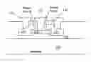
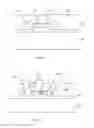
BRIEF DESCRIPTION OF THE DRAWINGSFIG. 1 is a side cross sectional view of a one-time programmable memory cell of this invention.
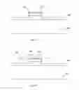
FIGS. 2A to 2G are a serial of side cross sectional views for illustrating the processing steps for manufacturing the OTP memory cell of FIG. 1.
DETAILED DESCRIPTION OF THE METHODReferring to FIG. 1 for a one-time programmable memory cell of this invention supported on a thick field oxide layer 100 formed on a top surface of a semiconductor substrate 100. The thick field oxide layer 105 insulates the cell from the substrate 100. A first doped poly region 210 is insulted with a thin layer low voltage gate oxide 120 from a second doped polysilicon region 125. Each poly region has an electrode, e.g., electrodes 135 and 140 respectively, connected for data recording and reading. The thin gate oxide layer 120 between the two doped poly regions blocks the conductivity between the two doped poly regions 110 and 125. However, the conducting status between the two doped poly regions 110 and 125 may be changed for the purpose of programming the memory. In the process of programming the memory cell as shown in FIG. 1, a high voltage may be applied to the electrodes between doped poly regions 110 and 125. When the voltage is high enough, a breakdown is induced in the single crystal thin gate oxide layer 120 and becomes conductive. The high voltage therefore changes the conductance between the two doped poly regions 110 and 125 and is employed to store a binary bit in the cell. The threshold voltage is related to the thickness as well as the micro microstructure of the oxide layer 120.
The key features as that shown in FIG. 1 are the relative positions of the second polysilicon poly-2 segment 125 over the first polysilicon poly-1 segment. The sidewall overlaying the poly-1 segment 110 includes a corner undercut. With the undercut and edge effects of the thin oxide layer 120 as sidewall covering the poly-1 segment 110, a breakdown can be conveniently induced and the state of conductivity can be more easily changed for writing a binary bit into the memory cell by applying a high voltage over the electrodes 135 and 140.
Referring to FIGS. 2A to 2F for a serial of side cross sectional views for the illustration of the processing steps to fabricate the one-time programmable memory cell of FIG. 1. In FIG. 2A, a field oxide layer 205 of approximately three to eight Angstrom thickness is formed on top of a semiconductor substrate 200 by using a thermal oxidation process. In FIG. 2B, a polysilicon layer 210 of approximately 500 to 2000 Angstroms in layer thickness is deposited on top of the field oxide layer 205. A N-type or P-type ion implant with an ion flux intensity of approximately 1×10¹⁴ to 1×10¹⁵/cm2 is then carried out over the polysilicon layer 210 to make the poly-1 more conductive. A mask is then applied to etch and pattern the polysilicon layer 210 to form a poly-1 segment 210 as shown. A high voltage oxide layer 215 is grown over the poly-1 segment.
In FIG. 2C, the high voltage oxide layer 215 is etched off in the active cell area and maintaining the high voltage oxide layer in the peripheral region to support the high voltage recording operation. The etch process produces an undercut 218 below the edge of the poly-1 segment 210. In FIG. 2D, a thin layer of low voltage oxide 220 of approximately 120 Angstroms in thickness is grown over the poly-1 segment 210. In FIG. 2E, a second polysilicon layer 225 is deposited. An ion implant is carried out on the second polysilicon layer 225 with a similar dopant concentration with either a N-type or P-type ions. Then a mask is applied to etch and pattern the second polysilicon layer 225 as that shown in FIG. 2E. In FIG. 2F, an oxide or BPSG layer 230 is deposited over the top to cover the entire top surface. Then in FIG. 2G, a contact mask is applied to open contact holes in the BPSG layer 230 and the metal contact is then deposited into the contact openings to form the electrodes 235 and 240 for establishing electric contacts to the doped poly-1 and poly 2 layers 210 and 225 respectively.
Although the present invention has been described in terms of the presently preferred embodiment, it is to be understood that such disclosure is not to be interpreted as limiting. Various alterations and modifications will no doubt become apparent to those skilled in the art after reading the above disclosure. Accordingly, it is intended that the appended claims be interpreted as covering all alterations and modifications as fall within the true spirit and scope of the invention.
Claims
We claim:1. A one-time programmable (OTP) memory cell comprising:
a dielectric layer disposed between two conductive polysilicon segments wherein said dielectric layer is ready to change from a non-conductive state to a conductive state through an induced voltage breakdown.
2. The one-time programmable (OTP) memory cell of claim 1 wherein:
one of said conductive polysilicon segments further includes an etch undercut configuration for conveniently inducing said voltage breakdown in said dielectric layer.
3. The one-time programmable (OTP) memory cell of claim 1 wherein:
one of said conductive polysilicon segments further includes an etch undercut configuration for conveniently inducing said voltage breakdown in said dielectric layer via a corner electrical field effect.
4. The one-time programmable (OTP) memory cell of claim 1 wherein:
said dielectric layer constituting a sidewall covering one of said conductive polysilicon segments with an etch undercut configuration for inducing said voltage breakdown in said dielectric layer via an edge electrical field effect.
5. The one-time programmable (OTP) memory cell of claim 1 wherein:
one of said conductive polysilicon segments further includes a corner for conveniently inducing said voltage breakdown in said dielectric layer via a corner electrical field effect.
6. The one-time programmable (OTP) memory cell of claim 1 further comprising:
a semiconductor substrate having an insulating layer disposed on a top surface of said substrate for supporting said OTP memory cell thereon.
7. The one-time programmable (OTP) memory cell of claim 1 further comprising:
an insulating passivation layer covering said OTP memory cell and said insulating passivation layer further includes contact opening for depositing electrode metal therein to for electrically contacting said conductive polysilicon segments to function as electrodes.
8. The one-time programmable (OTP) memory cell of claim 1 wherein:
said conductive polysilicon segments comprising conductive impurity doped polysilicon segments.
9. The one-time programmable (OTP) memory cell of claim 1 wherein:
at least one of said conductive polysilicon segments comprising N-type impurity doped polysilicon segments.
10. The one-time programmable (OTP) memory cell of claim 1 wherein:
at least one of said conductive polysilicon segments comprising P-type impurity doped polysilicon segments.
11. A method for manufacturing a one-time programmable (OTP) memory cell comprising:
disposing a dielectric layer between two conductive polysilicon segments for readily inducing a voltage breakdown in said dielectric to change from a non-conductive state to a conductive state for carrying out a one-time program operation.
12. The method of claim 11 further comprising:
forming one of said conductive polysilicon segments with an etch undercut configuration for conveniently inducing said voltage breakdown in said dielectric layer.
13. The method of claim 11 further comprising:
forming one of said conductive polysilicon segments with an etch undercut configuration with a corner for conveniently inducing said voltage breakdown in said dielectric layer via a corner electrical field effect.
14. The method of claim 11 further comprising:
forming one of said dielectric layer as a sidewall covering one of said conductive polysilicon segments with an etch undercut configuration for inducing said voltage breakdown in said dielectric layer via an edge electrical field effect.
15. The method of claim 11 further comprising:
forming one of said conductive polysilicon segments with a corner for conveniently inducing said voltage breakdown in said dielectric layer via a corner electrical field effect.
Images & Drawings included:
Sources:
- United States Patent and Trademark Office - verify current appl. status at the USPTO↗
Similar patent applications:
- » 20160078962
Anti-fuse type one-time programmable memory cell and anti-fuse type one-time programmable memory cell arrays - » 14572127
Anti-fuse type one-time programmable memory cell and anti-fuse type one-time programmable memory cell arrays - » 15262376
Anti-fuse one-time programmable memory cell and anti-fuse one-time programmable memory array - » 20100284210
One-time programmable memory cell - » 20090168486
Large capacity one-time programmable memory cell using metal oxides - » 20060044861
System and method using a one-time programmable memory cell - » 20070041246
Method using a one-time programmable memory cell - » 20080247242
Method using a one-time programmable memory cell - » 20050162892
One-time programmable memory cell - » 20090237975
One-time programmable memory cell
Recent applications in this class:
- » 20250292849 2025-09-18
REFERENCE RESISTOR HAVING VARIABLE RESISTANCE - » 20250266113 2025-08-21
MEMORY CIRCUIT AND METHOD OF OPERATING SAME - » 20250253004 2025-08-07
One-Time Programmable (OTP) Memory and Method of Operating the Same - » 20250246253 2025-07-31
MEMORY DEVICE, INTEGRATED CIRCUIT AND OPERATING METHOD OF MEMORY DEVICE - » 20250232825 2025-07-17
SEMICONDUCTOR DEVICE STRUCTURE - » 20250210120 2025-06-26
POWER CONDITIONING CIRCUIT FOR IN-FIELD FUSE PROGRAMMING - » 20250191666 2025-06-12
MERGED BIT LINES FOR HIGH DENSITY MEMORY ARRAY - » 20250182835 2025-06-05
SEMICONDUCTOR MEMORY DEVICES WITH DIODE-CONNECTED MOS - » 20250140328 2025-05-01
NON-VOLATILE MEMORY DEVICE HAVING A FUSE TYPE MEMORY CELL ARRAY - » 20250124992 2025-04-17
ONE-TIME PROGRAMMABLE BITCELL FOR FRONTSIDE AND BACKSIDE POWER INTERCONNECT