Method for fabricating CMOS image sensor
US20060273363A1
2006-12-07
11/448,426
2006-06-07
✅ Patent granted
US 7,491,991 B2
2009-02-17
-
-
Laura M Menz
2026-10-12
Abstract:
A method for fabricating a CMOS image sensor is provided. The method includes: forming a gate electrode with a gate insulating layer interposed on a transistor region of a semiconductor substrate having an active region defined by a photo diode and a transistor region; forming a first impurity region of a first conductive type at a transistor region at one side of the gate electrode; forming a second impurity region of a first conductive type at a photo diode region at other side of the gate electrode; forming sidewall insulating layers at both sides of the gate electrode; forming a third impurity region of a first conductive type at one side of a gate electrode where the first impurity region is formed; and forming a fourth impurity region of a second conductive type at the gate electrode, the photodiode region and the transistor region by implanting impurity ions of a second conductive type on the entire surface of the semiconductor substrate.
Assignee:
- Dongbu Electronics Co., Ltd. 766 🇰🇷 Seoul, South Korea
Interested in similar patents?
Get notified when new applications in this technology area are published.
Classification:
H01L27/14643 » CPC main
Devices consisting of a plurality of semiconductor or other solid-state components formed in or on a common substrate including semiconductor components sensitive to infra-red radiation, light, electromagnetic radiation of shorter wavelength or corpuscular radiation and specially adapted either for the conversion of the energy of such radiation into electrical energy or for the control of electrical energy by such radiation; Devices controlled by radiation; Imager structures Photodiode arrays; MOS imagers
H01L27/14689 » CPC further
Devices consisting of a plurality of semiconductor or other solid-state components formed in or on a common substrate including semiconductor components sensitive to infra-red radiation, light, electromagnetic radiation of shorter wavelength or corpuscular radiation and specially adapted either for the conversion of the energy of such radiation into electrical energy or for the control of electrical energy by such radiation; Devices controlled by radiation; Imager structures; Processes or apparatus peculiar to the manufacture or treatment of these devices or parts thereof MOS based technologies
H01L31/113 IPC
Semiconductor devices sensitive to infra-red radiation, light, electromagnetic radiation of shorter wavelength or corpuscular radiation and specially adapted either for the conversion of the energy of such radiation into electrical energy or for the control of electrical energy by such radiation; Processes or apparatus specially adapted for the manufacture or treatment thereof or of parts thereof; Details thereof in which radiation controls flow of current through the device, e.g. photoresistors characterised by at least one potential-jump barrier or surface barrier, e.g. phototransistors; Devices sensitive to infra-red, visible or ultra-violet radiation characterised by field-effect operation, e.g. junction field-effect phototransistor being of the conductor-insulator-semiconductor type, e.g. metal-insulator-semiconductor field-effect transistor
H01L21/00 IPC
Processes or apparatus adapted for the manufacture or treatment of semiconductor or solid state devices or of parts thereof
Description
RELATED APPLICATIONThis application claims the benefit, under 35 U.S.C. §119(e), of Korean Patent Application No. 10-2005-0048480 filed Jun. 7, 2005, which is incorporated herein by reference in its entirety.
FIELD OF THE INVENTIONThe present invention relates to a method for fabricating a CMOS image sensor.
BACKGROUND OF THE INVENTIONGenerally, an image sensor is a semiconductor device that transforms an optical image to an electric signal. An image sensor can be classified as a charge coupled device (CCD) or a complementary metal oxide silicon (CMOS) image sensor.
The CCD has shortcomings such as a complicated driving method and high power consumption. Also, the fabricating method of the CCD is complicated because a multi-level photo process is required.
Therefore, the CMOS image sensor has received attention as a next-generation image sensor to overcome the shortcomings of the CCD.
The CMOS image sensor is a device employing a switching mode that sequentially detects outputs of each unit pixel using MOS transistors. The switching mode can incorporate MOS transistors formed on a semiconductor substrate in a number at least as many as the number of unit pixels, and can use a control circuit and a signal processing circuit as peripheral circuits.
The CMOS image sensor can be classified into types such as a 3T type, a 4T type, and a 5T type, according the number of transistors. For example, the 3T type CMOS image sensor includes one photodiode and three transistors, and the 4T type CMOS image sensor includes one photodiode and four transistors.
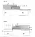
Hereinafter, the unit pixel of the 4T type CMOS image sensor will be described with reference to a plan view thereof.
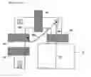
As shown in FIG. 1, the unit pixel of the CMOS image sensor according to the prior art includes a photodiode 10 and four transistors as an optoelectric converter. The four transistors are a transfer transistor 20, a reset transistor 30, an access transistor 40 and a select transistor 50. In FIG. 1, FD denotes a floating diffusion region and a numeral reference 90 denotes a coupling portion connecting the FD and the access transistor 40. Vin denotes an input terminal, and Vout denotes an output terminal.
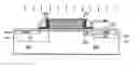
Hereinafter, the photodiode 10 and the transfer transistor 20 in the CMOS image sensor according to the prior art will be described with reference to a cross-section view through line I-I′.
As shown in FIG. 2, the transfer transistor 20 includes a gate insulating layer 21 and a gate electrode 23 formed on a substrate 11, and a first sidewall 29 and a second sidewall 31 formed at both sides of the gate electrode 23.
In addition an n− type diffusion region (N−) 28 and a Po type diffusion region (PDP; P type photodiode implant) 35 are formed at the photodiode region (PD) of the substrate 11. The Po type diffusion region 35 is formed on the n− type diffusion region 28. Also, a heavily doped n+ type diffusion region (N+) 32 and a lightly doped n− type diffusion region (N−) 26 are formed at the floating diffusion region (FD) of the substrate 11.
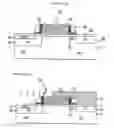
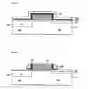
FIG. 3 is a cross-sectional view for describing one of processes for fabricating a CMOS image sensor according to the prior art.
As shown in FIG. 3, a photoresist layer 34 can be applied on an entire surface of the substrate 11, and the applied photoresist layer 27 can be patterned to expose the photodiode region (PD) through an exposing and developing process.
Then, a Po type diffusion region 35 can be formed in the n− type diffusion region 28 of the photodiode region by implanting Po type impurity ions using the patterned photoresist layer 34 as a hard mask.
However, the method for fabricating a CMOS image sensor according to the prior art has problems as follows.
The relevant art's fabricating method becomes complicated because a photolithography process, which includes applying a photoresist layer, exposing and developing the photoresist layer, implanting impurity ions, and removing the photoresist layer, is performed in order to form the Po type diffusion region (PDP) at the photodiode region.
SUMMARY OF THE INVENTIONAccordingly, the present invention is directed to a method for fabricating a CMOS image sensor that can address one or more problems of the prior art.
An object of the present invention is to provide a method for fabricating a CMOS image sensor that can improve yield by simplifying a fabricating process through omitting a photolithography process when ion implantation is performed for forming a PDP.
Another object of the present invention is to provide a method for fabricating a CMOS image sensor that can improve quality of the CMOS sensor by omitting a fabricating process that may create impurities through omitting a photolithography process when ion implantation is performed for forming a PDP.
Additional advantages, objects, and features of the invention will be set forth in part in the description which follows and in part will become apparent to those having ordinary skill in the art upon examination of the following or may be learned from practice of the invention. The objectives and other advantages of the invention may be realized and attained by the structure particularly pointed out in the written description and claims hereof as well as the appended drawings.
To achieve these objects and other advantages and in accordance with the purpose of the invention, as embodied and broadly described herein, there is provided a method of fabricating a CMOS image sensor, the method including: forming a gate electrode with a gate insulating layer interposed on a transistor region of a semiconductor substrate having an active region defined by a photo diode and a transistor region; forming a first impurity region of a first conductive type at a transistor region at one side of the gate electrode; forming a second impurity region of a first conductive type at a photo diode region at the other side of the gate electrode; forming sidewall insulating layers at both sides of the gate electrode; forming a third impurity region of a first conductive type at one side of a gate electrode where the first impurity region is formed; and forming a fourth impurity region of a second conductive type at the gate electrode, the photodiode region, and the transistor region by implanting a second conductive impurity ion on the entire surface of the semiconductor substrate.
It is to be understood that both the foregoing general description and the following detailed description of the present invention are exemplary and explanatory and are intended to provide further explanation of the invention as claimed.
BRIEF DESCRIPTION OF THE DRAWINGSThe accompanying drawings, which are included to provide a further understanding of the invention and are incorporated in and constitute a part of this application, illustrate embodiment(s) of the invention and together with the description serve to explain the principle of the invention. In the drawings:
FIG. 1 is a plan view of a unit pixel in a 4T type CMOS image sensor according to the prior art;
FIG. 2 is a cross-sectional view taken along the line I-I′ of FIG. 1 for showing a photodiode and a transfer gate;
FIG. 3 is a cross-sectional view for describing one of the processes for fabricating a CMOS image sensor according to the prior art; and
FIGS. 4A through 4H are cross-sectional views for describing a method for fabricating a CMOS image sensor according to an embodiment of the present invention.
DETAILED DESCRIPTION OF THE INVENTIONReference will now be made in detail to the preferred embodiments of the present invention, examples of which are illustrated in the accompanying drawings. Wherever possible, the same reference numbers will be used throughout the drawings to refer to the same or like parts.
Hereinafter, a method for fabricating a CMOS image sensor according to the present invention will be described with reference to accompanying drawings.
In the CMOS image sensor according to an embodiment of the present invention, a transfer transistor can have, for example, an NMOS transistor structure. However, the transfer transistor can alternatively have a PMOS type structure.
An embodiment of the present invention relates to a method for fabricating a CMOS image sensor having four transistors. However, the embodiment of the present invention can be applied to a method for fabricating a CMOS image sensor having other numbers of transistors such as one, three, five, or more transistors.
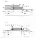
FIGS. 4A through 4H are cross-sectional views for illustrating a CMOS image sensor according to an embodiment of the present invention.
As shown in FIG. 4A, a substrate 111 can incorporate a lightly doped P type epitaxial layer by performing an epitaxial process on a semiconductor substrate such as heavily doped P++ type mono crystal silicon.
An epitaxial layer is formed in order to improve the capability of a low-voltage photodiode for accumulating photo-charge and to improve photo sensitivity thereof by greatly and deeply forming the depletion region at the photodiode.
In addition, a P-well can be formed in the substrate 111 by ion implantation.
Then, a gate insulating layer 112 and a conductive layer, for example, a heavily doped poly silicon layer, can be formed in sequence. Gate electrode 113 can then be formed by selectively removing the conductive layer through a photo and etching process.
In an embodiment, the gate insulating layer 112 can be formed by performing a thermal oxidation process or a chemical vapor deposition (CVD) on the semiconductor substrate.
In a further embodiment, the gate electrode can be formed by forming a silicide layer (not shown) on the conductive layer.
As shown in FIG. 4B, an oxide layer 114 can be formed on the gate electrode 113. In a specific embodiment, about 60 Å and less of a thermal oxide layer 114 can be formed on the surface of the gate electrode 113. The oxide layer 114 can function as a sidewall of a gate for implanting ion for source/drain of a transistor.
Also, the oxide layer 114 can effectively block Po type impurity ions from being implanted into the gate electrode 113 during Po type impurity ion implantation for forming the Po type diffusion region (PDP) 124.
As shown in FIG. 4C, a first photoresist layer 115 is applied on the substrate 111, and the first photoresist layer 115 is patterned to cover the photodiode region and to expose the floating diffusion region.
Then, an n− type diffusion region 116 is formed by implanting lightly doped n− type impurity ions at the exposed floating diffusion region using the patterned first photoresist layer 115 as a hard mask.
As shown in FIG. 4D, after the first photoresist layer 115 is removed, a second photoresist layer 117 is applied on the entire surface of the substrate 111 and patterned to expose the photodiode region through an exposing and developing process.
A lightly doped n− type diffusion region (PDN) 118 is formed at the photodiode region by implanting lightly doped n− type impurity ions at ion implanting energy of about 100 KeV to 500 KeV using the patterned second photoresist layer 117 as a hard mask.
The impurity ion implantation for forming the lightly doped n− type diffusion region 118 at the photodiode region is performed at higher energy than that for forming the lightly doped n− type diffusion region 116 at the floating diffusion region in order to form the lightly doped n− type diffusion region 118 more deeply.
As shown in FIG. 4E, the second photoresist layer 117 is removed, and a first insulating layer 119a and a second insulating layer 120a are sequentially formed on the entire substrate 111 through chemical vapor deposition or low voltage chemical vapor deposition.
In an embodiment, the first insulating layer 119a can be an oxide layer, and the second insulating layer 120a can be a nitride layer 120a.
In a specific embodiment, the first insulating layer 119a can be formed to a thickness of about 150 Å to 250 Å, and the second insulating layer 120a can be formed to a thickness of about 700 Å to 900 Å.
As shown in FIG. 4F, a first sidewall layer 119 and a second sidewall layer 120 are formed at both sides of the gate electrode 113 by performing an etch-back of the first insulating layer 119a and the second insulating layer 120a.
As shown in FIG. 4G, a third photoresist layer 121 is applied on the substrate 111 and is patterned to remain on the photodiode region through an exposing and developing process.
Then, an n+ type diffusion region 122 is formed at the floating diffusion region by implanting heavily doped n+ impurity ions using the patterned third photoresist layer 121 as a hard mask.
As shown in FIG. 4H, the third photoresist layer 121 is removed, and a Po type diffusion region (PDP) 124 is formed at the n− type diffusion region 118 of the photodiode region by implanting Po type impurity ion on the entire surface of the substrate using the first sidewall insulating layer 119 and the second sidewall insulating layer 120 as a hard mask.
Although the Po type impurity ion can be implanted into the n+ type diffusion region 122 when the Po type diffusion region 124 is formed, it does not influence the performance of the transistor.
For embodiments incorporating the oxide layer 114 formed on the gate electrode 113, the oxide layer 114 can effectively block the Po type impurity ions from being implanted into the gate electrode 113.
Moreover, implantation dose and implantation energy can be used to ensure that transistor characteristics are protected from influence of the Po type impurity ions. For example, for the Po type impurity ions that are implanted into the gate electrode 113 of the transistor, the characteristics of the transistor can still be protected by controlling the ion impurity dose and the implanting energy.
In embodiments of the subject method, BF2 or Boron can be used as an impurity ion source.
When BF2 is implanted as the impurity ion source, the ion implantation can be performed at a dose of 1×10¹¹ to 5×10¹² atoms/cm2 with the ion implanting energy of 40 KeV and less such that the dopant concentration is about 1×10¹⁶ to 5×10¹⁷ atoms/cm3.
When Boron is implanted as the impurity ion source, the ion implantation can be performed at a dose of 1×10¹¹ to 5×10¹² atoms/cm2 with the ion implanting energy of 10 KeV and less such that the dopant concentration is about 1×10¹⁶ to 5×10¹⁷ atoms/cm3.
Accordingly, the characteristics of a transistor can be protected from being influenced controlling the impurity ion dose and the implanting energy when the Po impurity ions are implanted. In addition, the fabrication process can be simplified by performing the ion implantation through controlling the impurity ion dose and the implanting energy without performing a photolithography process when the PDP ion is implanted at the photodiode region.
In a further embodiment, a thermal process, for example, a rapid thermal process, can be performed on the semiconductor substrate at a temperature of about 800° C. to 1200° C. to diffuse the impurity ions in the n− type diffusion region 116, the Po type diffusion region 124, the n− type diffusion region 118, and the n+ type diffusion region 122.
According to the present invention, a fabricating process can be simplified by performing the ion implantation through controlling the impurity ion dose and the implanting energy without performing a photolithography process when a PDP ion is implanted at the photodiode region.
According to the present invention, the CMOS image sensor having high quality can be fabricated by skipping a process that can create impurities through omitting a photolithography process when the PDP ion implanted in the fabricating process for the CMOS image sensor.
It will be apparent to those skilled in the art that various modifications and variations can be made in the present invention. Thus, it is intended that the present invention covers the modifications and variations of the invention provided they come within the scope of the appended claims and their equivalents.
Claims
I claim:1. A method for fabricating a CMOS image sensor comprising:
forming a gate electrode with a gate insulating layer interposed on a transistor region of a semiconductor substrate having an active region defined by a photo diode and the transistor region;
forming a first impurity region of a first conductive type at the transistor region at a first side of the gate electrode;
forming a second impurity region of the first conductive type at the photo diode region at a second side of the gate electrode;
forming sidewalls comprising a first insulating layer and a second insulating layer at the first side and the second side of the gate electrode;
forming a third impurity region of the first conductive type at the first side of the gate electrode where the first impurity region is formed; and
forming a fourth impurity region of a second conductive type by implanting impurity ions of a second conductive type on the gate electrode, the photodiode region and the transistor region.
2. The method according to claim 1, wherein the second impurity region is formed deeper in the substrate than the first impurity region.
3. The method according to claim 1, further comprising forming 60 Å and less of an oxide layer on a top and side surfaces of the gate electrode.
4. The method according to claim 1, wherein forming the first impurity region comprises forming a lightly doped n− type diffusion region by implanting impurity ions of an n type at the transistor region.
5. The method according to claim 1, wherein forming the second impurity region comprises forming a lightly doped n− type diffusion region by implanting impurity ions of an n type into the photodiode region at an ion implanting energy of 100 KeV to 500 KeV.
6. The method according to claim 1, wherein forming the third impurity region comprises forming a n+ type diffusion region by implanting impurity ions of the n type at the transistor region of the substrate.
7. The method according to claim 1, wherein forming the fourth impurity region comprises forming a Po diffusion region on the second impurity region and the third impurity region by implanting Po impurity ions into the entire substrate using the sidewalls as a hard mask.
8. The method according to claim 1, wherein forming the fourth impurity region comprises forming a Po diffusion region on the second impurity region, the third impurity region, and the gate electrode by implanting Po impurity ion into the entire substrate using the sidewalls as a hard mask.
9. The method according to claim 1, wherein the impurity ions of the second conductive type are BF2.
10. The method according to claim 9, wherein the implantation dose of the BF2 ion is 1×10¹¹ atoms/cm2 to 5×10¹² atoms/cm2.
11. The method according to claim 9, wherein the ion implanting energy is about 40 KeV and less for implanting the BF2 ions.
12. The method according to claim 9, wherein the dopant concentration of the fourth impurity region is 1×10¹⁶ atoms/cm3 to 5×10¹⁷ atoms/cm3.
13. The method according to claim 1, wherein the impurity ions of the second conductive type are boron.
14. The method according to claim 13, wherein the implantation dose of the boron ion is 1×10¹¹ atoms/cm2 to 5×10¹² atoms/cm2.
15. The method according to claim 13, wherein ion implanting energy is 10 KeV and less for implanting the boron ions.
16. The method according to claim 13, wherein the dopant concentration of the fourth impurity region is 1×10¹⁶ atoms/cm3 to 5×10¹⁷ atoms/cm3.
17. The method according to claim 1, further comprising performing a thermal process on the substrate after forming the fourth impurity region.
18. The method according to claim 1, wherein the first insulating layer is 150 Å to 250 Å and the second insulating layer is 700 Å to 900 Å.
19. The method according to claim 1, wherein forming the sidewalls comprises:
sequentially depositing the first insulating layer and the second insulating layer; and
performing an etch-back process on the first insulating layer and the second insulating layer.
20. The method according to claim 1, further comprising forming an oxide layer on the gate electrode of about 60 Å and less.
Images & Drawings included:
Sources:
- United States Patent and Trademark Office - verify current appl. status at the USPTO↗
Similar patent applications:
- » 20150243701
CMOS image sensors having a transfer gate electrode, and methods of fabricating CMOS image sensors having a transfer gate electrode - » 20120001241
CMOS Image Sensor Including PNP Triple Layer And Method Of Fabricating The CMOS Image Sensor - » 20060110873
Method for fabricating CMOS image sensor - » 20060001043
CMOS image sensor and fabricating method thereof - » 20060003519
Method for fabricating CMOS image sensor - » 20060019425
Method for fabricating CMOS image sensor - » 20050093088
Isolation layer for CMOS image sensor and fabrication method thereof - » 20050090035
Method for fabricating CMOS image sensor protecting low temperature oxide delamination - » 10831815
Pinned photodiode for a CMOS image sensor and fabricating method thereof - » 20050266625
CMOS image sensor and fabricating method thereof
Recent applications in this class:
- » 20250072133 2025-02-27
PHOTODETECTOR AND FORMING METHOD THEREOF - » 20250063833 2025-02-20
IMAGE SENSOR - » 20250048753 2025-02-06
CHANNEL PATTERN DESIGN TO IMPROVE CARRIER TRANSFER EFFICIENCY - » 20250048752 2025-02-06
Image Sensor Architectures that Employ Multi-Potential Dynamic Substrate Biasing - » 20250015120 2025-01-09
DETECTION DEVICE - » 20250006770 2025-01-02
COMPLEMENTARY METAL-OXIDE-SEMICONDUCTOR IMAGE SENSING DEVICES - » 20240387598 2024-11-21
PHOTOELECTRIC CONVERSION DEVICE, SYSTEM USING PHOTOELECTRIC CONVERSION DEVICE, AND MOVING BODY - » 20240387597 2024-11-21
IMAGE SENSOR - » 20240387596 2024-11-21
IMAGE SENSOR DEVICES AND METHODS OF FORMATION - » 20240379724 2024-11-14
CAPPING STRUCTURE TO REDUCE DARK CURRENT IN IMAGE SENSORS
Recent applications for this Assignee:
- » 20100314675 2010-12-16
Power semiconductor device and method for manufacturing the same - » 20100133421 2010-06-03
Complementary metal oxide silicon image sensor and method of fabricating the same - » 20100029051 2010-02-04
Semiconductor device and fabricating method thereof - » 20100019353 2010-01-28
Semiconductor device and method for manufacturing the same - » 20090317953 2009-12-24
Memory device and method for manufacturing the same - » 20090317952 2009-12-24
Memory device and method for manufacturing the same - » 20090317949 2009-12-24
ESD protecting circuit and manufacturing method thereof - » 20090302361 2009-12-10
Complementary metal oxide semiconductor (CMOS) image sensor - » 20090278205 2009-11-12
High voltage BICMOS device and method for manufacturing the same - » 20090273032 2009-11-05
LDMOS device and method for manufacturing the same