Peelable tape carrier
US20060275585A1
2006-12-07
11/397,235
2006-04-04
✅ Patent granted
US 8,173,245 B2
2012-05-08
-
-
Donald J Loney
2028-04-08
Abstract:
A support tape used in semiconductor wafer processing that includes an adhesive tape and a plurality of spaced support ribs arranged on the adhesive tape.
Inventors:
- Robert Montgomery 2 🇬🇧 Marshfield, United Kingdom
- Robert Montgomery 10 🇬🇧 South Glamorgan, United Kingdom
Assignee:
- INTERNATIONAL RECTIFIER CORPORATION 879 🇺🇸 EL SEGUNDO, CA, United States
Interested in similar patents?
Get notified when new applications in this technology area are published.
Classification:
H01L21/6836 » CPC main
Processes or apparatus adapted for the manufacture or treatment of semiconductor or solid state devices or of parts thereof; Apparatus specially adapted for handling semiconductor or electric solid state devices during manufacture or treatment thereof; Apparatus specially adapted for handling wafers during manufacture or treatment of semiconductor or electric solid state devices or components ; Apparatus not specifically provided for elsewhere for supporting or gripping using temporarily an auxiliary support Wafer tapes, e.g. grinding or dicing support tapes
C09J7/22 » CPC further
Adhesives in the form of films or foils characterised by their carriers Plastics; Metallised plastics
H01L21/6835 » CPC further
Processes or apparatus adapted for the manufacture or treatment of semiconductor or solid state devices or of parts thereof; Apparatus specially adapted for handling semiconductor or electric solid state devices during manufacture or treatment thereof; Apparatus specially adapted for handling wafers during manufacture or treatment of semiconductor or electric solid state devices or components ; Apparatus not specifically provided for elsewhere for supporting or gripping using temporarily an auxiliary support
C09J2203/326 » CPC further
Applications of adhesives in processes or use of adhesives in the form of films or foils for bonding electronic components such as wafers, chips or semiconductors
H01L21/78 » CPC further
Processes or apparatus adapted for the manufacture or treatment of semiconductor or solid state devices or of parts thereof; Manufacture or treatment of devices consisting of a plurality of solid state components formed in or on a common substrate or of parts thereof; Manufacture of integrated circuit devices or of parts thereof; Manufacture or treatment of devices consisting of a plurality of solid state components or integrated circuits formed in, or on, a common substrate with subsequent division of the substrate into plural individual devices
H01L2221/68327 » CPC further
Processes or apparatus adapted for the manufacture or treatment of semiconductor or solid state devices or of parts thereof covered by; Apparatus for handling semiconductor or electric solid state devices during manufacture or treatment thereof; Apparatus for handling wafers during manufacture or treatment of semiconductor or electric solid state devices or components; Apparatus not specifically provided for elsewhere for supporting or gripping using temporarily an auxiliary support used during dicing or grinding
H01L2221/6834 » CPC further
Processes or apparatus adapted for the manufacture or treatment of semiconductor or solid state devices or of parts thereof covered by; Apparatus for handling semiconductor or electric solid state devices during manufacture or treatment thereof; Apparatus for handling wafers during manufacture or treatment of semiconductor or electric solid state devices or components; Apparatus not specifically provided for elsewhere for supporting or gripping using temporarily an auxiliary support used to protect an active side of a device or wafer
Y10T428/2457 » CPC further
Stock material or miscellaneous articles; Structurally defined web or sheet [e.g., overall dimension, etc.] including variation in thickness Parallel ribs and/or grooves
Y10T428/24612 » CPC further
Stock material or miscellaneous articles; Structurally defined web or sheet [e.g., overall dimension, etc.] including variation in thickness Composite web or sheet
Y10T428/24942 » CPC further
Stock material or miscellaneous articles; Structurally defined web or sheet [e.g., overall dimension, etc.] including components having same physical characteristic in differing degree
Y10T428/24992 » CPC further
Stock material or miscellaneous articles; Structurally defined web or sheet [e.g., overall dimension, etc.] including components having same physical characteristic in differing degree Density or compression of components
Y10T428/28 » CPC further
Stock material or miscellaneous articles Web or sheet containing structurally defined element or component and having an adhesive outermost layer
Y10T428/2848 » CPC further
Stock material or miscellaneous articles; Web or sheet containing structurally defined element or component and having an adhesive outermost layer Three or more layers
H01L2924/0002 » CPC further
Indexing scheme for arrangements or methods for connecting or disconnecting semiconductor or solid-state bodies as covered by; Technical content checked by a classifier Not covered by any one of groups , and
H01L2924/00 » CPC further
Indexing scheme for arrangements or methods for connecting or disconnecting semiconductor or solid-state bodies as covered by
B32B3/30 IPC
Layered products comprising a layer with external or internal discontinuities or unevennesses, or a layer of non-planar form ; Layered products having particular features of form characterised by a particular shape of the outline of the cross-section of a continuous layer; characterised by a layer with cavities or internal voids ; characterised by an apertured layer characterised by a layer formed with recesses or projections, e.g. hollows, grooves, protuberances, ribs
B32B3/00 IPC
Layered products comprising a layer with external or internal discontinuities or unevennesses, or a layer of non-planar form ; Layered products having particular features of form
H01L23/32 IPC
Details of semiconductor or other solid state devices Holders for supporting the complete device in operation, i.e. detachable fixtures
Description
RELATED APPLICATIONThis application is based on and claims benefit of U.S. Provisional Application No. 60/686,183, filed on Jun. 1, 2005, entitled Semi-Rigid Peelable Tape Carrier for Thinned Semiconductor Wafers, to which a claim of priority is hereby made and the disclosure of which is incorporated by reference.
BACKGROUND OF THE INVENTIONThe present invention relates to semiconductor processing, and more particularly to a support tape for use in the processing of a semiconductor wafer.
Semiconductor device die are usually formed in a relatively large wafer (e.g. six inches in diameter), and then singulated from the wafer by sawing or the like.
In some cases, the wafers are relatively thick (e.g. 300 microns or more), and can be conveniently handled without breakage by processing tools such as ion implanters, photolithography tools, etching and cleaning equipment, metal deposition and insulation deposition equipment and the like.
It is known that in some cases, the characteristics of the semiconductor device can be improved if the wafer is thinned to, for example, below 250 microns, or even 100 microns or less. Also, it is known that it may be economical to form certain semiconductor devices in float zone type wafers and then thin the wafer to obtain thin semiconductor devices.
Wafers can be thinned by back grinding after the major wafer processing steps are completed. For example, wafers can be thinned to 80 microns or less after the top surface processing has been completed. For example, after the top surface processing is completed, a flexible tape is adhered to the processed front side of the wafer and the back side is suitably ground to the desired thickness. The flexible tape may be a plastic film of the kind commercially known as backgrind tape, which holds the wafer during the thinning process. The backgrind tape is peelable from the wafer.
In the case of thinned wafers, as the wafer is thinned it loses rigidity. Thus, it becomes difficult to handle the wafer. For example, it becomes difficult to remove the wafer from the grinding system without breaking the wafer. Excessive breakage negatively affects the yield and adversely affects any cost savings that may have been achieved by the wafer thinning method.
To overcome the problem, the prior art has suggested either using a more rigid carrier backing or a rigid carrier. A more rigid backing, however, does not bend or fold easily, making it difficult to remove from the thinned wafer without causing damage to the same. Also, rigid carriers are more complex to use since the carrier must be attached with an adhesive and will be very hard to remove without consequent damage to the thinned wafer.
SUMMARY OF THE INVENTIONIt is an object of the present invention to reduce the number of incidents of breakage of thinned wafers.
A support tape according to the present invention exhibits a higher resistance to bending or folding in one direction, while exhibiting a relatively lower resistance to bending or folding in the peeling direction.
A support tape according to the present invention includes an adhesive tape having an adhesive on one surface thereof, and a plurality of spaced support ribs arranged opposite the adhesive. The support ribs are more rigid than the adhesive tape. As a result, a support tape according to the present invention is less resistant to bending or folding in at least one direction compared to other directions of bending or folding. The use of a support tape according to the present invention, therefore, allows, for example, a thinned wafer to be handled by the grinding machine (or other processing apparatus), while also allowing the tape to be peeled away from the wafer with a lessened likelihood of breakage.
Other features and advantages of the present invention will become apparent from the following description of the invention which refers to the accompanying drawings.
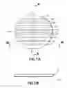
BRIEF DESCRIPTION OF THE FIGURESFIG. 1A schematically shows a top plan view of a support tape according to the present invention.
FIG. 1B schematically shows a cross-sectional view of a support tape according to the present invention along line IB-IB and viewed in the direction of the arrows.
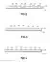
FIG. 2 schematically shows a cross-sectional view of a support tape according to the first embodiment of the present invention as would be seen along line A-A of FIG. 1A in the direction of the arrows.
FIG. 3 schematically shows a cross-sectional view of a support tape according to the second embodiment of the present invention as would be seen along line A-A in the direction of the arrows.
FIG. 4 schematically shows a cross-sectional view of a support tape according to the third embodiment of the present invention as would be seen along line A-A in FIG. 1A in the direction of the arrows.
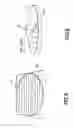
FIG. 5 schematically illustrates the application of a support tape according to the present invention to a wafer.
FIG. 6 schematically illustrates the peeling of a support tape according to the present invention from a wafer.
DETAILED DESCRIPTION OF THE FIGURESReferring to FIGS. 1A-1B, support tape 10 according to the present invention includes adhesive tape 12 having an adhesive 16 on one surface thereof, and a plurality of spaced and preferably parallel support ribs 14 arranged opposite adhesive 16. According to the present invention adhesive tape 12 has a first rigidity value and each support rib 14 has a second rigidity value, which is higher than the first rigidity value. As a result, support tape 10 according to the present invention exhibits more rigidity when subjected to folding or bending action around axis Y (which is generally orthogonal to support ribs 14) than when subjected to bending or folding action around axis X (which is generally parallel to the direction of elongation of support ribs 14). Thus, due to the spacing between support ribs 14, adhesive tape 12 between support ribs 14 bends easily when being peeled in a direction that is generally orthogonal to support ribs 14.
Referring to FIG. 2, according to the first embodiment of the present invention, support ribs 14 are thickened regions integral with adhesive tape 12 and forming a unitary body with the same. Thus, support ribs 14 in the first embodiment of the present invention, due to their enlarged dimensions, are more rigid compared to adhesive tape 12 portion of support tape 10.
Referring next to FIG. 3, a support tape according to the second embodiment of the present invention includes support ribs 14 made from a material that is different from the material forming adhesive tape 12. That is, support ribs 14 may be made from a material that is inherently more rigid than the material forming the body of adhesive tape 12. Support ribs 14 in the second embodiment of the present invention may be attached to adhesive tape 12 with any suitable adhesive, or fused with the same to form an integrated body.
Referring next to FIG. 4, according to the third embodiment, support ribs 14 are embedded in the body of adhesive tape 12. Preferably, support ribs 14 are made from a material that is inherently more rigid than a material forming the body of adhesive tape 12.
Preferably, adhesive tape 12 is made from the same material that is used to form a conventional backgrind tape, although other materials for forming adhesive tape 12 can be used without deviating from the spirit and scope of the present invention. Also, support ribs 14 may be preferably made from any suitable plastic material, although other materials may be used without deviating from the spirit and cope of the present invention. In addition, adhesive 16 may be preferably any suitable pressure sensitive adhesive rendering a support tape according to the present invention readily peelable from a semiconductor wafer, although other types of adhesives such as UV activated, UV releasable, or heat-activated, or heat-releasable adhesives may be used to form adhesive 16 without deviating from the scope and spirit of the present invention.
Referring next to FIG. 5, a support tape 10 according to the present invention as applied to a wafer 18 will give wafer 18 enough rigidity in one direction so that wafer 18 does not sag when held in a standard cassette 20. As a result, the handling of a thin wafer (e.g. 100 mm thick or thinner wafer) can be improved. Note that a support tape according to the present invention is applied to a wafer 18 prior to the thinning of wafer 18 and thereafter remains adhered to wafer 18 in order to facilitate its handling.
Referring next to FIG. 6, a support tape 10 according to the present invention can then be peeled off from wafer 18 after thinning in a direction orthogonal to support ribs 14 as described above.
Note that the primary function of adhesive tape 12 is to render mechanical support to the wafer during the back grinding operation, and preferably, unlike dicing tape, adhesive tape 12 is not expandable. For example, when processing a wafer containing a plurality of vertical conduction power devices such as vertical conduction type MOSFETs, adhesive tape 12 is attached to the front side of the wafer and the wafer is thinned by grinding from the backside. The thinned wafer can then be removed and singulated by, for example, dicing. In another variation, the wafer can be singulated prior to the removal of adhesive tape 12.
Alternatively, the wafer can be partially diced. That is, for example, the front side of the wafer is diced but not all the way through its thickness. The adhesive tape 12 is then attached to the wafer and the portion which has not been diced is removed by grinding or the like process, whereby the die are singulated. Preferably adhesive tape 12 is rendered mechanically rigid enough for dicing before grinding as described above.
Although the present invention has been described in relation to particular embodiments thereof, many other variations and modifications and other uses will become apparent to those skilled in the art. It is preferred, therefore, that the present invention be limited not by the specific disclosure herein, but only by the appended claims.
Claims
What is claimed is:1. A support tape comprising:
an adhesive tape having a first rigidity value and an adhesive on a first surface thereof; and
a plurality of spaced support ribs arranged opposite said adhesive and having a second rigidity value, wherein said second rigidity value is higher than said first rigidity value.
2. The support tape of claim 1, wherein said spaced ribs parallel one another.
3. The support tape of claim 1, wherein said adhesive is pressure sensitive.
4. The support tape of claim 1, wherein said adhesive is configured to be peelable from a semiconductor wafer.
5. The support tape of claim 1, wherein said adhesive tape is comprised of backgrind tape.
6. The support tape of claim 1, wherein said ribs are integrated with said tape.
7. The support tape of claim 1, wherein said adhesive tape and said ribs are comprised of dissimilar materials.
8. The support tape of claim 1, wherein said ribs are comprised of rigid plastic.
9. The support tape of claim 1, wherein said ribs are thickened regions of said adhesive tape rendering said ribs more rigid than said adhesive tape.
10. The support tape of claim 1, wherein said ribs are coupled to said adhesive tape.
11. The support tape of claim 1, wherein said ribs and said adhesive tape are integrated.
12. The support tape of claim 1, wherein said ribs are embedded in said adhesive tape.
13. The support tape of claim 1, wherein said adhesive is UV activated.
14. The support tape of claim 1, wherein said adhesive is heat activated.
15. The support tape of claim 1, wherein said adhesive is UV releasable.
16. The support tape of claim 1, wherein said adhesive is heat releasable.
Images & Drawings included:

Sources:
- United States Patent and Trademark Office - verify current appl. status at the USPTO↗
Recent applications in this class:
- » 20250293077 2025-09-18
FILM ADHESIVE, DICING AND DIE-BONDING INTEGRAL FILM, SEMICONDUCTOR DEVICE, AND MANUFACTURING METHOD FOR SAME - » 20250293076 2025-09-18
METHOD FOR PRODUCING SEMICONDUCTOR DEVICE - » 20250293075 2025-09-18
DIE BONDING FILM AND METHOD FOR MANUFACTURING SAME, DICING/DIE BONDING INTEGRATED FILM AND METHOD FOR MANUFACTURING SAME, AND METHOD FOR MANUFACTURING SEMICONDUCTOR DEVICE - » 20250293074 2025-09-18
METHOD FOR PRODUCING SEMICONDUCTOR DEVICE, AND EXPANDABLE TAPE - » 20250285905 2025-09-11
SEMICONDUCTOR PACKAGE AND MANUFACTURING METHOD THEREOF - » 20250273503 2025-08-28
METHOD FOR MANUFACTURING SEMICONDUCTOR DEVICE, AND ADHESIVE FILM FOR SEMICONDUCTOR WAFER PROCESSING - » 20250273502 2025-08-28
FILM FOR TEMPORARY FIXATION, LAYERED PRODUCT FOR TEMPORARY FIXATION, AND METHOD FOR PRODUCING SEMICONDUCTOR DEVICE - » 20250266282 2025-08-21
METHOD OF TRANSPORTING SEMICONDUCTOR DEVICE AND CARRIER TAPE - » 20250253183 2025-08-07
PRESSURE-SENSITIVE ADHESIVE TAPE FOR SEMICONDUCTOR WAFER PROCESSING - » 20250253182 2025-08-07
METHOD FOR MANUFACTURING SEMICONDUCTOR DEVICE
Recent applications for this Assignee:
- » 20150130036 2015-05-14
Semiconductor package with low profile switch node integrated heat spreader - » 20150037965 2015-02-05
Fabrication of III-nitride semiconductor device and related structures - » 20150008572 2015-01-08
Power semiconductor package with multiple dies - » 20150001599 2015-01-01
Power semiconductor package with non-contiguous, multi-section conductive carrier - » 20140353680 2014-12-04
Gallium nitride semiconductor structures with compositionally-graded transition layer - » 20140339686 2014-11-20
Group III-V device with a selectively modified impurity concentration - » 20140339651 2014-11-20
Semiconductor device with a field plate double trench having a thick bottom dielectric - » 20140332879 2014-11-13
Power semiconductor device with reduced on-resistance and increased breakdown voltage - » 20140327014 2014-11-06
III-nitride rectifier package - » 20140319665 2014-10-30
Power semiconductor package