Display panels
US20060279510A1
2006-12-14
11/181,469
2005-07-14
✅ Patent granted
US 8,159,443 B2
2012-04-17
-
-
Alexander Eisen | Christopher E Leiby
2028-06-17
Abstract:
A display panel comprising a plurality of first and second signal lines, first and second detecting lines, a plurality of ESD protection circuits, and first and second common electrode lines. The first and second detecting lines are respectively coupled to the first signal lines and the second signal lines. Each ESD protection circuit is coupled to one of the first signal lines or one of the second signal lines. The first and second common electrode lines are respectively coupled to first and second voltage ports. Each first signal line is coupled to the first common electrode line through the corresponding ESD protection circuit. Each second signal line is coupled to the second common electrode line through the corresponding ESD protection circuit.
Assignee:
- AU OPTRONICS CORP. 966 🇹🇼 Hsinchu, Taiwan
Interested in similar patents?
Get notified when new applications in this technology area are published.
Classification:
G09G3/006 » CPC main
Control arrangements or circuits, of interest only in connection with visual indicators other than cathode-ray tubes Electronic inspection or testing of displays and display drivers, e.g. of LED or LCD displays
G09G3/3648 » CPC further
Control arrangements or circuits, of interest only in connection with visual indicators other than cathode-ray tubes for presentation of an assembly of a number of characters, e.g. a page, by composing the assembly by combination of individual elements arranged in a matrix no fixed position being assigned to or needed to be assigned to the individual characters or partial characters by control of light from an independent source using liquid crystals; Control of matrices with row and column drivers using an active matrix
G09G2330/04 » CPC further
Aspects of power supply; Aspects of display protection and defect management Display protection
H01L27/0248 » CPC further
Devices consisting of a plurality of semiconductor or other solid-state components formed in or on a common substrate including semiconductor components specially adapted for rectifying, oscillating, amplifying or switching and having at least one potential-jump barrier or surface barrier; including integrated passive circuit elements with at least one potential-jump barrier or surface barrier; Particular design considerations for integrated circuits for electrical or thermal protection, e.g. electrostatic discharge [ESD] protection
G09G3/36 IPC
Control arrangements or circuits, of interest only in connection with visual indicators other than cathode-ray tubes for presentation of an assembly of a number of characters, e.g. a page, by composing the assembly by combination of individual elements arranged in a matrix no fixed position being assigned to or needed to be assigned to the individual characters or partial characters by control of light from an independent source using liquid crystals
Description
BACKGROUNDThe invention relates to a liquid crystal display panel, and in particular to a liquid crystal display panel with a test circuit.
FIG. 1 is a schematic diagram of a display array of a conventional liquid crystal display (LCD) panel. As shown in FIG. 1, a display array 1, formed by interlacing data lines D1 to Dm and scan lines G1 to Gn, is configured on a glass substrate and Each interlaced data line and scan line corresponds to one display unit, for example, interlaced data line D1 and scan line S1 correspond to display unit 100. As with any other display unit, the equivalent circuit of the display unit 100 comprises a switch transistor TFT, a storage capacitor Cs, and a liquid crystal capacitor Clc. A gate of the switch transistor is coupled to the scan line G1, and a drain thereof is coupled to the data line D1, and a source thereof is coupled to a pixel electrode PE.
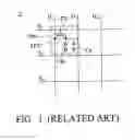
After the display array of the LCD panel having the above-described configuration is formed, the glass substrate is tested to detect shorts and breaks in the data lines D1 to Dm and the scan lines G1 to Gn. To complete these tests, a liquid crystal display (LCD) device for testing signal line disclosed in U.S. Pat. No. 6,566,902 B2, as shown in FIG. 2, comprises a plurality of data lines DL, an odd-numbered detecting line ODDL, and an even-numbered detecting line EDDL. The odd-numbered detecting line ODDL is commonly connected to odd-numbered data lines DL through data pads 2, and the even-numbered detecting line EDDL is commonly connected to even-numbered data lines DL through data pads 2. The LCD device provides two common electrode lines CLa and CLb arranged on the LCD device to cross each data line DL. The LCD also provides a plurality of electrostatic discharge (ESD) protection circuits 12, each connected between an odd-numbered data line and the common electrode line CLa and between an even-numbered data line and the common electrode line CLb. The LCD device further provides at least two auxiliary ESD protection circuits 14 connected in series between the two separated common electrode lines CLa and CLb. In this LCD device, one common voltage source Vcom provides voltage to both common electrode lines CLa and CLb. In a test process, test signals are applied to the odd-numbered detecting line ODDL and the even-numbered detecting line EDDL and then to the odd-numbered data lines and the even-numbered data lines, respectively, to thereby detect faults of the data lines DL, such as a short between two adjacent data lines DL. Similarly, the same test configuration is employed in the scan lines.
In the related art, the data lines DL are connected to the common electrode lines CLa or CLb through ESD protection circuits 12, which are further connected to the same common voltage source Vcom through auxiliary ESD protection circuits 14. Thus, the test signals on the odd-numbered detecting line ODDL and the even-numbered detecting line EDDL interfere with each other in a test process, resulting in an inaccurate test of signal lines.
SUMMARYDisplay panels are provided. An exemplary embodiment of a display panel comprises a plurality of first signal lines, a plurality of second signal lines, a first detecting line, a second detecting line, a plurality of ESD protection circuits, a first common electrode line, and a second common electrode line. The second signal lines are alternately configured with the first signal lines. The first detecting line is coupled to the first signal lines. The second detecting line is coupled to the second signal lines. Each ESD protection circuit is coupled to one of the first signal lines or one of the second signal lines. The first common electrode line is coupled to a first voltage port. The second common electrode line is coupled to a second voltage port. Each first signal line is coupled to the first common electrode line through the corresponding ESD protection circuit. Each second signal line is coupled to the second common electrode line through the corresponding ESD protection circuit.
In some embodiments, a first impedance element is coupled between the first common electrode line and the first voltage port. A second impedance element is coupled between the second common electrode line and the second voltage port. The first and second signal lines can be data lines or scan lines.
DESCRIPTION OF THE DRAWINGSThe invention will become more fully understood from the detailed description given hereinbelow and the accompanying drawings, given by way of illustration only and thus not intended to be limitative of the invention.
FIG. 1 shows a conventional display array of a LCD panel.
FIG. 2 shows a LCD device for testing signal line disclosed in U.S. Pat. No. 6,566,902 B2.
FIGS. 3 and 4 depict an embodiment of a display panel.
FIG. 5 depicts an embodiment of a display panel.
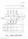
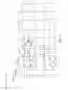
DETAILED DESCRIPTIONDisplay panels are provided. In some embodiments, as shown in FIG. 3, a display panel 3 comprises a test circuit 30 and a display array 31 configured on a glass substrate. Since the display array 31 in FIG. 3 is the same as the display array 1 in FIG. 1, like reference numbers are used to designate like parts, and descriptions of the like parts are omitted here. In the embodiment of FIG. 3, the display array 31 is formed by interlacing data lines D1 to D2, and scan lines G1 to G2y. The data lines D1 to D2x are divided into two groups, one comprising the odd-numbered data lines D1 to D2x-1, and the other comprising the even-numbered data lines D2 to D2x. The test circuit 30 comprises an odd-numbered detecting line ODDL1, an even-numbered detecting line EDDL1, a plurality of electrostatic discharge (ESD) protection circuits 301, and a plurality of data pads 302. The odd-numbered data lines D1 to D2x-1 are coupled to the odd-numbered detecting line ODDL1 through corresponding data pads 302, and the even-numbered data lines D2 to D2x are coupled to the even-numbered detecting line EDDL1 through corresponding data pads 302.
Each ESD protection circuit 301 is coupled between the odd-numbered data lines D1 to D2x-1 and a common electrode line CL1 or between the even-numbered data lines D2 to D2x and a common electrode line CL2. Note that the common electrode lines CL1 and CL2 are coupled to different common voltage ports. As shown in FIG. 3, the common electrode line CL1 is coupled to a common voltage port PV1, while the common electrode line CL2 is coupled to a common voltage port PV2.
In the embodiment of FIG. 3, a high impedance element R1 is coupled between the common electrode line CL1 and the common voltage port PV1, and a high impedance element R2 is coupled between the common electrode line CL2 and the common voltage port PV2.
On the glass substrate, the common voltage ports PV1 and PV2 are different, that is, the common voltage ports PV1 and PV2 are not coupled on the glass substrate. Thus, in a test process, respective test signals provided to the odd-numbered data lines D1 to D2x-1 and the even-numbered data lines D2 to D2x do not interfere with each other.
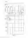
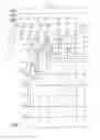
Referring to FIG. 4, the display panel 3 further comprises a test circuit 32 for testing the scan lines S1 to S2y. For clarity, FIG. 4 shows only the test circuit 32 and the display array 31, and the test circuit 31 is omitted. Referring FIG. 4, the scan lines S1 to S2y are divided into two groups, one comprising the odd-numbered scan lines S1 to S2y-1, and the other comprising the even-numbered scan lines S2 to S2y. The test circuit 32 comprises an odd-numbered detecting line ODDL2, an even-numbered detecting line EDDL2, a plurality of ESD protection circuits 303, and a plurality of scan pad 304. The odd-numbered scan lines S1 to S2y-1 are coupled to the odd-numbered detecting line ODDL2 through corresponding scan pads 304, and the even-numbered scan lines S2 to S2y are coupled to the even-numbered detecting line EDDL2 through corresponding scan pads 304.
Each ESD protection circuit 303 is coupled between the odd-numbered scan lines S1 to S2y-1 and a common electrode line CL3 or between the even-numbered scan lines S2 to Sy and a common electrode line CL4. Note that the common electrode lines CL3 and CL4 are coupled to different common voltage ports. As shown in FIG. 4, the common electrode line CL3 is coupled to a common voltage port PV3, while the common electrode line CL4 is coupled to a common voltage port PV4.
In the embodiment of FIG. 4, a high impedance element R3 is coupled between the common electrode line CL3 and the common voltage port PV3, and a high impedance element R4 is coupled between the common electrode line CL4 and the common voltage port PV4.
On the glass substrate, the common voltage ports PV3 and PV4 are different, that is, the common voltage ports PV3 and PV4 are not coupled on the glass substrate. Thus, in a test process, respective test signals provided to the odd-numbered scan lines S1 to S2y-1 and the even-numbered scan lines S2 to S2y do not interfere with each other.
In some embodiments, as shown in FIG. 5, a display panel 5 comprises a test circuit 50 and a display array 51 configured on a glass substrate. Since the display array 51 in FIG. 5 is the same as the display array 1 in FIG. 1, like reference numbers are used to designate like parts, and the description of like parts are omitted here. In the embodiment of FIG. 5, the display array 51 is formed by interlacing data lines D1 to D3x and scan lines G1 to G23. According to the three primary colors, red (R) green (G), and blue (B), the data lines D1 to D3x are divided into three groups, one comprising red data lines D1 to D3x-2, another comprising green data lines D2 to D3x-1, and another comprising blue data lines D3 to D3x. The test circuit 50 comprises a red detecting line RDDL, green detecting line GDDL, a blue detecting line BDDL, a plurality of ESD protection circuits 501, and a plurality of data pad 502. The red data lines D1 to D3x-2 are coupled to the red detecting line RDDL through corresponding data pads 502, the green data lines D2 to D3x-1 are coupled to the green detecting line GDDL through corresponding data pads 502, and the blue data lines D3 to D3x are coupled to the blue detecting line BDDL through corresponding data pads 502.
Each ESD protection circuit 501 is coupled between the red data lines D1 to D3x-2 and a common electrode line CLR, between the green data lines D2 to D3x-1 and a common electrode line CLG, or between the blue data lines D3 to D3x and a common electrode line CLB. Note that the common electrode lines CLR, CLG, and CLB are coupled to different common voltage ports. As shown in FIG. 5, the common electrode line CLR is coupled to a common voltage port PVR, the common electrode line CLG is coupled to a common voltage port PVG, and the common electrode line CLB is coupled to a common voltage port PVB,
In the embodiment of FIG. 5, a high impedance element R is coupled between each common electrode line and the corresponding common voltage port.
On the glass substrate, the common voltage ports PVR, PVG, and PVB are different, that is, the common voltage ports PVR, PVG, and PVB are not coupled on the glass substrate. Thus, in a test process, respective test signals provided to the red data lines D1 to D3x-2, the green data lines D2 to D3x-1, and the blue data lines D3 to D3x do not interfere with each other.
In the embodiment of FIG. 5, a test circuit (not shown) for scan lines S1 to S2y is the same as the test current 32 in FIG. 4. Thus, the connection between the scan lines S1 to S2y and the corresponding test circuit refers to the description of FIG. 4 and further description is omitted here.
In the invention, according to system requirements, signal lines (data lines or scan lines) can be divided into a plurality of groups for testing. Each group of signal lines is coupled to one common electrode line. Since each common electrode line is coupled to a respective common voltage port on a glass substrate, test signals on the plurality of common electrode lines do not interfere with each other. Moreover, the plurality of common voltage ports are not connected on the glass substrate, but in the printed circuit board (PCB) or flexible printed circuit (FPC) outside the glass substrate.
While the invention has been described in terms of preferred embodiment, it is to be understood that the invention is not limited thereto. On the contrary, it is intended to cover various modifications and similar arrangements as would be apparent to those skilled in the art. Therefore, the scope of the appended claims should be accorded the broadest interpretation so as to encompass all such modifications and similar arrangements.
Claims
What is claimed is:1. A display panel comprising:
a plurality of first signal lines;
a plurality of second signal lines, alternately configured with the first signal lines;
a first detecting line coupled to the first signal lines;
a second detecting line coupled to the second signal lines;
a plurality of electrostatic discharge (ESD) protection circuits, each coupled to one of the first signal lines or one of the second signal lines;
a first common electrode line coupled to a first voltage port, wherein each first signal line is coupled to the first common electrode line through the corresponding ESD protection circuit; and
a second common electrode line coupled to a second voltage port, wherein each second signal line is coupled to the second common electrode line through the corresponding ESD protection circuit.
2. The display panel as claimed in claim 1, further comprising:
a first impedance element coupled between the first common electrode line and the first voltage port; and
a second impedance element coupled between the second common electrode line and the second voltage port.
3. The display panel as claimed in claim 1, wherein the first and second signal lines are data lines.
4. The display panel as claimed in claim 1, wherein the first and second signal lines are scan lines.
5. A display panel comprising:
alternately configured first, second, and third data lines;
a first detecting line coupled to the first data line;
a second detecting line coupled to the second data line;
a third detecting line coupled to the third data line;
a plurality of first electrostatic discharge (ESD) protection circuits, each coupled to the first, second, or third data lines;
a first common electrode line coupled to a first voltage port, wherein the first data line is coupled to the first common electrode line through the corresponding first ESD protection circuit;
a second common electrode line coupled to a second voltage port, wherein the second data line is coupled to the second common electrode line through the corresponding first ESD protection circuit; and
a third common electrode line coupled to a third voltage port, wherein the third data line is coupled to the third common electrode line through the corresponding first ESD protection circuit.
6. The display panel as claimed in claim 5, further comprising:
a first impedance element coupled between the first common electrode line and the first voltage port;
a second impedance element coupled between the second common electrode line and the second voltage port; and
a third impedance element coupled between the third common electrode line and the third voltage port.
7. The display panel as claimed in claim 5, further comprising:
first and second scan lines;
a fourth detecting line coupled to the first scan line;
a fifth detecting line coupled to the second scan line;
a plurality of second ESD protection circuits, each coupled to the first or second scan lines;
a fourth common electrode line coupled to a fourth voltage port, wherein the first scan line is coupled to the fourth common electrode line through the corresponding second ESD protection circuit; and
a fifth common electrode line coupled to a fifth voltage port, wherein the second scan line is coupled to the fifth common electrode line through the corresponding second ESD protection circuit.
8. The display panel as claimed in claim 7, further comprising:
a fourth impedance element coupled between the fourth common electrode line and the fourth voltage port; and
a fifth impedance element coupled between the fifth common electrode line and the fifth voltage port.
Images & Drawings included:
Sources:
- United States Patent and Trademark Office - verify current appl. status at the USPTO↗
Similar patent applications:
- » 20070258023
Dual-panel display panel, flat-panel display employing a dual-panel display panel, and method of showing images after the flat-panel display is turned off - » 20120300141
Lens panel, method for manufacturing the lens panel, display apparatus having the lens panel, display panel, a method for manufacturing the display panel and a display apparatus having the display panel - » 10446825
Display panel assembly, display panel case, display panel module, projection display device, and cooling method for the display panel module - » 20090225103
Driving device for display panel, display panel, display device including the driving device, and method for driving display panel - » 20230116030
Method of reducing color breakup of reflection of ambient light in display panel, display panel, display apparatus, and method of fabricating display panel - » 20110147751
DISPLAY PANEL SUBSTRATE, DISPLAY PANEL, METHOD FOR MANUFACTURING DISPLAY PANEL SUBSTRATE, AND METHOD FOR MANUFACTURING DISPLAY PANEL - » 20070126339
Method of manufacturing anode panel for flat-panel display device, method of manufacturing flat-panel display device, anode panel for flat-panel display device, and flat-panel display device - » 20080081533
METHOD OF MANUFACTURING ANODE PANEL FOR FLAT-PANEL DISPLAY DEVICE, METHOD OF MANUFACTURING FLAT-PANEL DISPLAY DEVICE, ANODE PANEL FOR FLAT-PANEL DISPLAY DEVICE, AND FLAT-PANEL DISPLAY DEVICE - » 20170084244
DISPLAY PANEL DRIVING APPARATUS, A METHOD OF DRIVING A DISPLAY PANEL USING THE DISPLAY PANEL DRIVING APPARATUS AND A DISPLAY APPARATUS HAVING THE DISPLAY PANEL DRIVING APPARATUS - » 20170186395
Display panel driving apparatus, a method of driving a display panel using the display panel driving apparatus and a display apparatus including the display panel driving apparatus
Recent applications in this class:
- » 20250292711 2025-09-18
DISPLAY APPARATUS AND METHOD OF DRIVING DISPLAY PANEL USING THE SAME - » 20250285570 2025-09-11
DRIVER CHIP, AND STATE SELF-TEST METHOD THEREFOR - » 20250285569 2025-09-11
LIGHT-EMITTING SUBSTRATE AND DISPLAY APPARATUS - » 20250285568 2025-09-11
METHOD OF TESTING COMPENSATION OPERATION AND COMPENSATION OPERATION TEST SYSTEM PERFORMING THE SAME - » 20250285567 2025-09-11
DISPLAY DEVICE AND METHOD OF DRIVING DISPLAY DEVICE - » 20250279020 2025-09-04
Display Device - » 20250279019 2025-09-04
DISPLAY SYSTEM AND METHOD OF OPERATING DISPLAY SYSTEM - » 20250279018 2025-09-04
FLEXIBLE VOLTAGE GATE HIGH (VGH) SETTING AND VOLTAGE CALIBRATION - » 20250273106 2025-08-28
ELECTRONIC PANEL AND ELECTRONIC APPARATUS INCLUDING THE SAME - » 20250273105 2025-08-28
APPARATUS AND METHOD FOR DETERMINING STATUS OF FLEXIBLE DISPLAY
Recent applications for this Assignee:
- » 20190354228 2019-11-21
Dual-mode capacitive touch display panel - » 20190011787 2019-01-10
Pixel structure and display panel using same - » 20180130887 2018-05-10
Electrode structure of a transistor for increasing and stabilizing current flowing through drain electrode to source electrode, and pixel structure and display apparatus comprising the same - » 20170315657 2017-11-02
Dual-mode capacitive touch display panel - » 20170186361 2017-06-29
Shift register and control method thereof - » 20160189798 2016-06-30
Shift register - » 20160055829 2016-02-25
Display panel of combining gate control signal and emitting control signal - » 20150237331 2015-08-20
3D image adjustment method and 3D display apparatus using the same - » 20150228243 2015-08-13
Display panel, gate driver and control method - » 20150192831 2015-07-09
Display panel and display device