Pad layouts of a printed circuit board
US20060294489A1
2006-12-28
11/472,975
2006-06-21
✅ Patent granted
US 7,448,016 B2
2008-11-04
-
-
Phallaka Kik
2026-12-13
Abstract:
A pad layout of a printed circuit board includes a first and a second pad symmetrically arranged on the PCB for cooperatively receiving either a first surface mounted component (SMC) or a second surface mounted component (SMC). Each of the SMCs includes a first footprint and a second footprint. The first pad has a polygonal shape corresponding to a minimum sized shape that accommodates both a shape of the first footprint of the first SMC and a shape of the first footprint of the second SMC. The second pad has a polygonal shape corresponding to a minimum sized shape that accommodates both a shape of the second footprint of the first SMC and a shape of the second footprint of the second SMC.
Assignee:
- HON HAI Precision Industry CO., LTD. 1,310 🇹🇼 Tu-Cheng City, Taiwan
- HON HAI PRECISION INDUSTRY CO., LTD. 2,357 🇹🇼 Tu-Cheng, Taipei Hsien, Taiwan
- Hong Fu Jin Precision Industry (Shenzhen) Co., Ltd. 90 🇨🇳 Bao-an District, Shenzhen, Guangdong Province, China
Interested in similar patents?
Get notified when new applications in this technology area are published.
Classification:
H05K1/00 IPC
Printed circuits
H05K1/00 IPC
Printed circuits
H05K1/111 » CPC main
Printed circuits; Details; Printed elements for providing electric connections to or between printed circuits Pads for surface mounting, e.g. lay-out
H05K1/111 » CPC main
Printed circuits; Details; Printed elements for providing electric connections to or between printed circuits Pads for surface mounting, e.g. lay-out
H05K1/0295 » CPC further
Printed circuits; Details; Programmable, customizable or modifiable circuits adapted for choosing between different types or different locations of mounted components
H05K1/0295 » CPC further
Printed circuits; Details; Programmable, customizable or modifiable circuits adapted for choosing between different types or different locations of mounted components
H05K2201/09381 » CPC further
Indexing scheme relating to printed circuits covered by; Shape and layout; Shape and layout details of conductors; Pads and lands Shape of non-curved single flat metallic pad, land or exposed part thereof; Shape of electrode of leadless component
H05K2201/09381 » CPC further
Indexing scheme relating to printed circuits covered by; Shape and layout; Shape and layout details of conductors; Pads and lands Shape of non-curved single flat metallic pad, land or exposed part thereof; Shape of electrode of leadless component
H05K2201/09954 » CPC further
Indexing scheme relating to printed circuits covered by; Shape and layout; Shape or layout details not covered by a single group of - More mounting possibilities, e.g. on same place of PCB, or by using different sets of edge pads
H05K2201/09954 » CPC further
Indexing scheme relating to printed circuits covered by; Shape and layout; Shape or layout details not covered by a single group of - More mounting possibilities, e.g. on same place of PCB, or by using different sets of edge pads
H05K2201/10636 » CPC further
Indexing scheme relating to printed circuits covered by; Details of components or other objects attached to or integrated in a printed circuit board; Details of electrical connections of non-printed components, e.g. special leads; Components characterised by their electrical contacts Leadless chip, e.g. chip capacitor or resistor
Y02P70/50 » CPC further
Climate change mitigation technologies in the production process for final industrial or consumer products Manufacturing or production processes characterised by the final manufactured product
Y02P70/50 » CPC further
Climate change mitigation technologies in the production process for final industrial or consumer products Manufacturing or production processes characterised by the final manufactured product
H01R12/00 IPC
Structural associations of a plurality of mutually-insulated electrical connecting elements, specially adapted for printed circuits, e.g. printed circuit boards [PCBs], flat or ribbon cables, or like generally planar structures, e.g. terminal strips, terminal blocks; Coupling devices specially adapted for printed circuits, flat or ribbon cables, or like generally planar structures; Terminals specially adapted for contact with, or insertion into, printed circuits, flat or ribbon cables, or like generally planar structures
Description
BACKGROUND1. Technical Field
The present invention relates to pad layouts of printed circuit boards (PCBs), and more particularly to a pad layout of a PCB which can readily and reliably receive surface mounted components (SMCs) thereon.
2. General Background
In general, SMCs, including resistors, capacitors, inductors and so on, are connected to a printed circuit board by pads. The pads are arranged on the printed circuit board in a matched relationship with footprints of the SMCs. The pads have different configurations due to varied configurations of the footprints of the SMCs, such as an ellipse, a circle, a square, a teardrop, and so on. Generally, however, the pad is only capable of receiving a certain SMC.
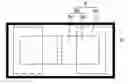
Referring to FIG. 2, a pad layout of a printed circuit board (PCB) using computer software (such as Protel) is for arranging SMCs, such as a 0805-type component 3, and a 0603-type component 5. A size of the 0805-type component 3 is larger than that of the 0603-type component 5. A pair of pads 8 each with an ellipse configuration is arranged on the PCB for receiving the 0805-type component 3. A pair of pads 6 each with an ellipse configuration is arranged on the PCB for receiving the 0603-type component 5. A lined frame 2 of the pads 8 is bigger than a lined frame 1 of the pads 6. A width W1 of the 0805-type component 3 is greater than a width W2 of the 0603-type component 5. A length of the 0805-type component 3 is L1. An outer distance L3 between the pads 8 is equal to an outer distance between footprints of the 0603-type component 3. An inner distance L5 between the pads 8 is equal to an inner distance between footprints of the 0805-type component 3. An inner distance L2 between the pads 6 is equal to an inner distance between footprints of the 0603-type component 5. Wherein L3>L5>L2, and W1>W2. The configuration of footprints of the 0803-type component 3 and the 0603-type component 5 are different. Therefore, each of these different SMCs require a different corresponding pad. The 0805-type component 3 and the 0603-type component 5 each have a pair of footprints corresponding to the pads 8 and pads 6 respectively. However, space on the printed circuit board is limited. Too many pads will decrease available space for electronic components and traces on the PCB causing difficulties to a layout engineer when he tries to selectively arrange multiple components on the PCB. Warnings 4 generated by the layout program may be frequent during the layout process further affecting the layout engineer's work.
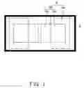
Referring to FIG. 3, showing another computer generated pad layout of a PCB, the PCB includes a pair of rectangular pads 7. Each of the pads 7 embraces configurations of the corresponding pads 8 and pads 6. An outer distance L33 between the pads 7 is equal to the distance L3 indicated in FIG. 2. An inner distance between the pads L23 is equal to the distance L2 indicated in FIG. 2. A width W13 of each of the pads 7 is equal to the width W1 indicated in the FIG.2. A length of each of the pads 32 can be concluded as (L33−L23)/2, that is, (L3−L2)/2. However, the surface area of the pads 7 is large, and during the soldering process smaller SMCs have a tendency to float on the melted solder. This causes an untidy appearance of the PCB and can lead to short-circuiting on the PCB. Besides, to include all configurations of the corresponding pads 8 and pads 6 in the pads 7 may also cost more.
What is needed is a pad layout on a PCB which can readily and reliably receive surface mounted components (SMCs) on the PCB.
SUMMARYAn exemplary pad layout of a printed circuit board includes a first and a second pad arranged on the PCB for cooperatively receiving either a first surface mounted component (SMC) or a second surface mounted component (SMC). Each of the SMCs includes a first footprint and a second footprint. The first pad has a polygonal shape corresponding to a minimum sized shape that accommodates both a shape of the first footprint of the first SMC and a shape of the first footprint of the second SMC. The second pad has a polygonal shape corresponding to a minimum sized shape that accommodates both a shape of the second footprint of the first SMC and a shape of the second footprint of the second SMC.
Other advantages and novel features will become more apparent from the following detailed description when taken in conjunction with the accompanying drawings, in which:
BRIEF DESCRIPTION OF THE DRAWINGSFIG. 1 is a plan view of a computer generated pad layout of a PCB in accordance with a preferred embodiment of the present invention; and
FIGS. 2 and 3 are plan views of conventional computer generated pad layouts of PCBs.
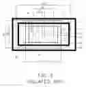
DETAILED DESCRIPTION OF THE EMBODIMENTSReferring to FIG. 1, a computer generated pad layout for a printed circuit board (PCB) according to a preferred embodiment of the present invention includes a pair of pads 9 for selectively receiving one of surface mounted components (SMCs) thereon. Referring also to FIG. 2, in the preferred embodiment, the pads 9 are for selectively receiving a 0805-type component 3 and a 0603-type component 5 thereon. The pair of pads 9 is arranged on the PCB. Each of the pads 9 is generally T-shaped, corresponding to a minimum sized shape that accommodates both a shape of the footprint of the 0805-type component 3 and a shape of the footprint of the 0603-type component 5.
By use of above described shapes, the surface area of the pads are minimized thereby reducing incidents of floating of small sized components, and reducing cost by minimizing materials used in manufacturing the pads. Further, in the design layout process of a PCB, by using pads shaped as described, a layout engineer will have more flexibility in solving issues related to limited space by having the freedom to design layouts that utilize more imaginative arrangements less dependent on the imposed symmetry of bulky large pads.
It is believed that the present embodiments and their advantages will be understood from the foregoing description, and it will be apparent that various changes may be made thereto without departing from the spirit and scope of the invention or sacrificing all of its material advantages, the examples hereinbefore described merely being preferred or exemplary embodiments.
Claims
What is claimed is:1. A pad layout on a printed circuit board (PCB) comprising:
a first and a second pad arranged on the PCB for cooperatively receiving either a first surface mounted component (SMC) or a second surface mounted component (SMC), each of the SMCs comprising a first footprint and a second footprint; wherein
the first pad has a polygonal shape corresponding to a minimum sized shape that accommodates both a shape of the first footprint of the first SMC and a shape of the first footprint of the second SMC; and
the second pad has a polygonal shape corresponding to a minimum sized shape that accommodates both a shape of the second footprint of the first SMC and a shape of the second footprint of the second SMC.
2. The pad layout as claimed in claim 1, wherein the polygonal shape of the first pad and the polygonal shape of the second pad are T-shaped.
3. The pad layout as claimed in claim 2, wherein the polygonal shape of the first pad comprises a first rectangle and a second rectangle over lapped with the first rectangle, the first rectangle circumscribes a corresponding the first footprint of the first SMC, the second rectangle circumscribes a corresponding first footprint of the second SMC.
4. The pad layout as claimed in claim 1, wherein the first polygons and the second polygons are rectangles, configurations of the footprints of the first and second SMCs are ellipses.
5. A pad layout on a printed circuit board (PCB) comprising:
two pads arranged on the PCB for selectively receiving a first surface mounted component (SMC) and a second surface mounted component (SMC), each of the SMCs comprising two footprints; and
each of the pads circumscribing a corresponding footprint of the first SMC and a corresponding footprint of the second SMC.
6. The pad layout as claimed in claim 5, wherein the polygonal shape of the first pad and the polygonal shape of the second pad are T-shaped.
Images & Drawings included:
Sources:
- United States Patent and Trademark Office - verify current appl. status at the USPTO↗
Similar patent applications:
Recent applications in this class:
- » 20250240886 2025-07-24
INTERPOSER FOR ACTIVE IMPLANTABLE MEDICAL DEVICE - » 20250227840 2025-07-10
FLEXIBLE PRINTED CIRCUIT BOARD, COF MODULE, AND ELECTRONIC DEVICE COMPRISING THE SAME - » 20250212329 2025-06-26
ELECTRONIC BOARD - » 20250203773 2025-06-19
SEMICONDUCTOR PACKAGE AND METHODS OF FORMATION - » 20250176105 2025-05-29
SELECTIVE TRANSFER OF MICRO DEVICES - » 20250176104 2025-05-29
PRINTED CIRCUIT BOARD AND SEMICONDUCTOR PACKAGE INCLUDING THE SAME - » 20250176103 2025-05-29
PRINTED CIRCUIT BOARD AND MANUFACTURING METHOD THEREOF - » 20250159805 2025-05-15
ELECTRONIC DEVICE - » 20250159804 2025-05-15
PRINTED CIRCUIT BOARD HAVING OPTIONAL CIRCUIT UNIT - » 20250159803 2025-05-15
CIRCUIT BOARD AND METHOD OF FABRICATING CIRCUIT BOARD
Recent applications for this Assignee:
- » 20140363586 2014-12-11
Laser-based method for growing an array of carbon nanotubes - » 20140299819 2014-10-09
Method for making a carbon nanotube film - » 20140199855 2014-07-17
Method for making a carbon nanotube film - » 20110171419 2011-07-14
Electronic element having carbon nanotubes - » 20110110535 2011-05-12
Carbon nanotube speaker - » 20110101832 2011-05-05
SECURING MECHANISM AND ELECTRONIC DEVICE ENCLOSURE USING THE SAME - » 20110096516 2011-04-28
SUPPORTING ASSEMBLY FOR PRINTED CIRCUIT BOARD - » 20110096473 2011-04-28
Electronic device - » 20110093746 2011-04-21
System and method for determining display function of BIOS error information - » 20110073276 2011-03-31
Heat dissipation system