Method for an element using two resist layers
US20070103379A1
2007-05-10
11/271,361
2005-11-10
✅ Patent granted
US 7,388,542 B2
2008-06-17
-
-
Hoang V. Nguyen
2026-03-17
Abstract:
A two resist layer process allows a seed layer to be used to electroplate a conductive layer of an element in a way that a portion of the seed layer can be removed.
Inventors:
- Robert R. Oberle 25 🇺🇸 Macungie, PA, United States
- Sandra M. Garby 1 🇺🇸 Bangor, PA, United States
Assignee:
- RCD TECHNOLOGY INC. 25 🇺🇸 QUAKERTOWN, PA, United States
Interested in similar patents?
Get notified when new applications in this technology area are published.
Classification:
H01Q1/2208 » CPC further
Details of, or arrangements associated with, antennas; Supports; Mounting means by structural association with other equipment or articles associated with components used in interrogation type services, i.e. in systems for information exchange between an interrogator/reader and a tag/transponder, e.g. in Radio Frequency Identification [RFID] systems
H01Q7/00 » CPC further
Loop antennas with a substantially uniform current distribution around the loop and having a directional radiation pattern in a plane perpendicular to the plane of the loop
H05K3/242 » CPC further
Apparatus or processes for manufacturing printed circuits; Secondary treatment of printed circuits; Reinforcing the conductive pattern characterised by the electroplating method; means therefor, e.g. baths or apparatus characterised by using temporary conductors on the printed circuit for electrically connecting areas which are to be electroplated
H05K1/095 » CPC further
Printed circuits; Details; Use of materials for the conductive, e.g. metallic pattern; Dispersed materials, e.g. conductive pastes or inks for polymer thick films, i.e. having a permanent organic polymeric binder
H05K1/095 » CPC further
Printed circuits; Details; Use of materials for the conductive, e.g. metallic pattern; Dispersed materials, e.g. conductive pastes or inks for polymer thick films, i.e. having a permanent organic polymeric binder
H05K1/165 » CPC further
Printed circuits incorporating printed electric components, e.g. printed resistor, capacitor, inductor incorporating printed inductors
H05K1/165 » CPC further
Printed circuits incorporating printed electric components, e.g. printed resistor, capacitor, inductor incorporating printed inductors
H05K3/048 » CPC further
Apparatus or processes for manufacturing printed circuits in which the conductive material is applied to the surface of the insulating support and is thereafter removed from such areas of the surface which are not intended for current conducting or shielding the conductive material being removed mechanically, e.g. by punching by selective transfer or selective detachment of a conductive layer using a lift-off resist pattern or a release layer pattern
H05K3/246 » CPC further
Apparatus or processes for manufacturing printed circuits; Secondary treatment of printed circuits; Reinforcing the conductive pattern; Reinforcing conductive patterns made by printing techniques or by other techniques for applying conductive pastes, inks or powders; Reinforcing other conductive patterns by such techniques Reinforcing conductive paste, ink or powder patterns by other methods, e.g. by plating
H05K2201/0347 » CPC further
Indexing scheme relating to printed circuits covered by; Conductive materials; Structure of the conductor; Layered conductors or foils Overplating, e.g. for reinforcing conductors or bumps; Plating over filled vias
H05K2201/0347 » CPC further
Indexing scheme relating to printed circuits covered by; Conductive materials; Structure of the conductor; Layered conductors or foils Overplating, e.g. for reinforcing conductors or bumps; Plating over filled vias
H05K2203/054 » CPC further
Indexing scheme relating to apparatus or processes for manufacturing printed circuits covered by; Patterning and lithography; Masks; Details of resist; Patterning and lithography Continuous temporary metal layer over resist, e.g. for selective electroplating
H05K2203/054 » CPC further
Indexing scheme relating to apparatus or processes for manufacturing printed circuits covered by; Patterning and lithography; Masks; Details of resist; Patterning and lithography Continuous temporary metal layer over resist, e.g. for selective electroplating
H05K2203/0574 » CPC further
Indexing scheme relating to apparatus or processes for manufacturing printed circuits covered by; Patterning and lithography; Masks; Details of resist; Details of resist Stacked resist layers used for different processes
H05K2203/0574 » CPC further
Indexing scheme relating to apparatus or processes for manufacturing printed circuits covered by; Patterning and lithography; Masks; Details of resist; Details of resist Stacked resist layers used for different processes
H05K2203/175 » CPC further
Indexing scheme relating to apparatus or processes for manufacturing printed circuits covered by; Post-manufacturing processes Configurations of connections suitable for easy deletion, e.g. modifiable circuits or temporary conductors for electroplating; Processes for deleting connections
Y10T29/49016 » CPC further
Metal working; Method of mechanical manufacture; Electrical device making Antenna or wave energy "plumbing" making
H01Q1/36 » CPC main
Details of, or arrangements associated with, antennas Structural form of radiating elements, e.g. cone, spiral, umbrella; Particular materials used therewith
H01P11/00 IPC
Apparatus or processes specially adapted for manufacturing waveguides or resonators, lines, or other devices of the waveguide type
H01Q1/38 IPC
Details of, or arrangements associated with, antennas; Structural form of radiating elements, e.g. cone, spiral, umbrella; Particular materials used therewith formed by a conductive layer on an insulating support
Description
BACKGROUND OF THE INVENTIONThe present invention relates to methods of manufacture of flexible circuits such as those used in construction of radio frequency (RF) antenna.
Radio frequency antenna are typically made in a conductive coil pattern. The conductive coil pattern allows the antenna to receive and radiate energies in the radio frequency range. Typically, the antenna is optimized to transmit and receive energy in a relatively narrow portion of the radio frequency range.
Radio frequency antenna are used in a number of different areas including inventory control. Often the radio frequency antenna is connected to an integrated circuit. The integrated circuit receives energy from a detector unit, modulates the energy with an identification pattern stored in the integrated circuit, and then retransmits the modulated energy to the detector unit. Such inventory control units, including the radio frequency antenna, can be made quite inexpensively.
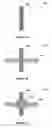
BRIEF DESCRIPTION OF THE DRAWINGSFIG. 1A-1E are diagrams of a method of producing an element, such as an RFID antenna.
FIG. 2 is a diagram illustrating the construction of a radio frequency antenna of the present invention using a two resist layer method.
DETAILED DESCRIPTION OF THE PREFERRED EMBODIMENTSFIG. 1A-1E show a method of forming an element, such as an RFID antenna. In FIG. 1A, a first resist layer 102 is put on a substrate 101. In one embodiment, the substrate 101 is a flexible substrate which allows the constructed radio frequency antenna or other element to bend. One example of a flexible substrate material which is suitable for use with the present invention is Mylar.RTM., polyester film from E.I. DuPont de Nemours, Wilmington, Del. The resist layers can be any type of non-conductive layer that can be formed on the substrate 101. In one embodiment, the resist is a liquid, such as the HEF-076HT resist available from the Englehard Corporation of Iselin, N.J.
In FIG. 1B, a seed layer 104 is placed over the first resist layer 102. The seed layer can be formed with a conductive ink. In one embodiment, the conductive ink is Spraylat XCMS-012. The conductive ink layer can be cured.
In FIG. 1C, a second resist layer 106 is formed over a portion of the seed layer 104. The second resist layer 106 can be made of the same material as the first resist layer 102.
In FIG. 1D, the exposed portion of the seed layer 104 is electroplated to form a conductive layer 108. The conductive layer is not formed on those portions of the seed layer 104 that is covered by the second resist layer 106. The seed layer 104 can keep point A and point B electrically connected such that a probe at point A can be used to electroplate point B and vice versa.
FIG. 1E shows the situation after the first and second resist layers are removed. The first and second resist layer can be removed with a stripping process. The portion of the seed layer that covers the first resist layer will also removed so that points A and B are now electrically isolated.
In one embodiment, resist layers and the insulating layer, are differentially removable (for example soluble in a solvent to which the initial seed layer is impervious) from the conductive ink material. The portion of the seed layer over the first resist layer will be undercut and thus removed along with the resist layers.
The conductive layer can be an inexpensive metal material. In one embodiment of the present invention, the conductive layer is made of copper. The stripping can be done using a solvent, ashing, reactive gas or any other method.
Point A can be part of a bus bar used for the construction of the element and point B can be part of the element, such as the RFID antenna.
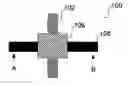
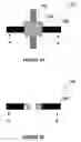
FIG. 2 shows an example of a substrate 202 with two antennas 204 and 206 formed upon it. The antennas shown in FIG. 2 are coil antennas. The antennas can also be dipole antennas, folded dipole antennas or another design. The temporary connection regions are shown with dotted lines.
The bus bar 208 can be used to electroplate over a seed layer. The method of the present invention can be used to temporarily connect the bus bar 208 with the antennas 204 and 206 in regions such as region 210. After the resist layer is stripped away, the electrical connection with the bus bar 208 is removed so that antennas 204 and 206 can be tested without interference.
Similarly, the method can be used to connect points, such as points 212, 214 and 216, that can allow the electroplating of the antennas, such as antenna 204, to be done evenly with the electrical connection completely removed when the two resist layers are stripped away.
Typically it is desired to minimize the resistance of the radio frequency antenna. A desirable property of radio frequency antenna is to have a relatively high Q factor. The Q factor for an antenna is defined as the imaginary over the real part of the impedance. The imaginary part of the impedance is typically a function of the desired operating frequency and geometry and is typically fixed. Thus, to produce a high Q factor antenna, the resistance of the antenna should be kept as small as possible. This means that it is desired to have a relatively thick conductive metal layer forming the coils of the radio frequency antenna. The use of the electrical-short layer aids in the construction of a uniformly thick electroplate layer, thus lowering the resistance and raising the Q factor.
The temporary connection can ensure that points on the conductive ink pattern will have relatively similar voltages during the electroplating process. This means all locations on the conductive ink pattern will be electroplated evenly. Thus the apparatus of one embodiment allows for a conductive electroplate layer of sufficient thickness on all points of the radio frequency antenna.
The use of the resist can allow for the use of a thinner and/or narrower conductive ink layer. The resistance of the conductive ink layer during the electroplate process is not as important of a factor because the electrical-short layer is used.
The above description is meant to be exemplary only. Additional ways of implementing the invention are done within the scope of the present invention, which is to be limited only by the appended claims.
Claims
What is claimed is:1. A method of forming an element, comprising:
forming a first resist layer on top of a substrate;
forming a seed layer on top of at least a portion of the first resist layer;
forming a second resist layer over a portion of the seed layer;
electroplating a conductive layer over exposed portions of the seed layer; and
removing the first and second resist.
2. The method of claim 1, wherein the element is an antenna.
3. The method of claim 1, wherein the seed layer has a coil pattern.
4. The method of claim 1, wherein after the removing step the conductive layer includes at least two electrically isolated regions.
5. The method of claim 1, wherein the electrically isolated regions are individual antenna elements.
6. The method of claim 1, wherein the seed layer comprises a conductive ink layer.
7. The method of claim 1, wherein the removing step comprises using a solvent to remove the first and second resist layers.
8. The method of claims 1, wherein the portion of the seed layer on top of the first resist layer electrically connects a bus bar to an antenna during the electroplating step.
9. The method of claim 1, wherein the portion of seed layer on top of the first resist layer shorts together portions of an antenna coil during the electroplating step.
10. The method of claim 1, wherein the portion of the seed layer on top of the first resist layer shorts together portions of a dipole antenna
11. An element constructed by the process of:
forming a first resist layer on top of a substrate;
forming a seed layer on top of at least a portion of the first resist layer;
forming a second resist layer over a portion of the seed layer;
electroplating a conductive layer over exposed portions of the seed layer; and
removing the first and second resist.
12. The element of claim 11, wherein the element is an antenna.
13. The element of claim 11, wherein the seed layer has a coil pattern.
14. The element of claim 11, wherein after the removing step the conductive layer includes at least two electrically isolated regions.
15. The element of claim 11, wherein the seed layer comprises a conductive ink layer.
16. The element of claim 11, wherein the removing step comprises using a solvent to remove the first and second resist layers.
17. The element of claims 11, wherein the portion of the seed layer on top of the first resist layer electrically connects a bus bar to an antenna during the electroplating step.
18. The element of claim 11, wherein the portion of seed layer on top of the first resist layer shorts together portion of an antenna coil during the electroplating step.
19. The element of claim 1 1, wherein the element has an exposed seed layer portion.
20. An RFID antenna constructed by the process of:
forming a first resist layer on top of a substrate;
forming a seed layer on top of at least a portion of the first resist layer;
forming a second resist layer over a portion of the seed layer;
electroplating a conductive layer over exposed portions of the seed layer; and
removing the first and second resist.
21. The RFID antenna of claim 20, wherein the element has an exposed seed layer portion.
Images & Drawings included:

Sources:
- United States Patent and Trademark Office - verify current appl. status at the USPTO↗
Recent applications in this class:
- » 20250174882 2025-05-29
ANTENNA STRUCTURES AND ANTENNA ASSEMBLIES THAT INCORPORATE THE ANTENNA STRUCTURES - » 20250062524 2025-02-20
BASE STATION ANTENNA, FEEDER COMPONENT AND FRAME COMPONENT - » 20240421471 2024-12-19
WIRING BOARD AND METHOD FOR MANUFACTURING WIRING BOARD - » 20240405414 2024-12-05
ELECTRONIC DEVICE - » 20240405413 2024-12-05
ANTENNA ELEMENT AND ANTENNA DEVICE - » 20240387985 2024-11-21
ANTENNA DEVICE - » 20240380102 2024-11-14
RADIATOR FOR PROVIDING TERAHERTZ ELECTROMAGNETIC RADIATION - » 20240363998 2024-10-31
IRRADIATION APPARATUS OF ELECTROMAGNETIC WAVES - » 20240347901 2024-10-17
Qc3 Healing Pyramid - » 20240275033 2024-08-15
ANTENNA MEMBER
Recent applications for this Assignee:
- » 20110234382 2011-09-29
Coupled radio frequency identification (RFID) and biometric device - » 20110057043 2011-03-10
Radio frequency identification (RFID) antenna with tuning stubs for mount on metal RFID tag - » 20100289626 2010-11-18
RADIO FREQUENCY IDENTIFICATION (RFID) ENABLED INVENTORY TRAY - » 20100271180 2010-10-28
RADIO FREQUENCY IDENTIFICATION (RFID) CREDENTIAL FOR GUEST SERVICES - » 20090315686 2009-12-24
RFID TAG USING ENCRYPTED VALUE - » 20090256762 2009-10-15
RFID ANTENNA WITH QUARTER WAVELENGTH SHUNT - » 20090128417 2009-05-21
ELECTROLESS/ELECTROLYTIC SEED LAYER PROCESS - » 20090128337 2009-05-21
RFID based keyboard - » 20090128333 2009-05-21
RFID inventory monitor - » 20090128295 2009-05-21
RFID based identification device