Laser-marking method for a wafer
US20070111346A1
2007-05-17
11/543,195
2006-10-05
Abstract:
The present invention relates to a laser-marking method for a wafer. The method of the invention comprises the steps of: (a) providing a wafer, the wafer having a first surface and a second surface, and a glue layer disposed on the first surface; (b) attaching the glue layer under a first film, the first film installed on a frame; and (c) projecting a laser light on the second surface of the wafer to mark the wafer. By utilizing the frame, the supporting force can be larger and orientation of the laser can be improved so as to improve the precision for marking the wafer and improve the quality of products.
Interested in similar patents?
Get notified when new applications in this technology area are published.
Classification:
H01L23/544 » CPC main
Details of semiconductor or other solid state devices Marks applied to semiconductor devices , e.g. registration marks,
H01L21/6835 » CPC further
Processes or apparatus adapted for the manufacture or treatment of semiconductor or solid state devices or of parts thereof; Apparatus specially adapted for handling semiconductor or electric solid state devices during manufacture or treatment thereof; Apparatus specially adapted for handling wafers during manufacture or treatment of semiconductor or electric solid state devices or components ; Apparatus not specifically provided for elsewhere for supporting or gripping using temporarily an auxiliary support
H01L21/6836 » CPC further
Processes or apparatus adapted for the manufacture or treatment of semiconductor or solid state devices or of parts thereof; Apparatus specially adapted for handling semiconductor or electric solid state devices during manufacture or treatment thereof; Apparatus specially adapted for handling wafers during manufacture or treatment of semiconductor or electric solid state devices or components ; Apparatus not specifically provided for elsewhere for supporting or gripping using temporarily an auxiliary support Wafer tapes, e.g. grinding or dicing support tapes
H01L21/78 » CPC further
Processes or apparatus adapted for the manufacture or treatment of semiconductor or solid state devices or of parts thereof; Manufacture or treatment of devices consisting of a plurality of solid state components formed in or on a common substrate or of parts thereof; Manufacture of integrated circuit devices or of parts thereof; Manufacture or treatment of devices consisting of a plurality of solid state components or integrated circuits formed in, or on, a common substrate with subsequent division of the substrate into plural individual devices
H01L2221/68327 » CPC further
Processes or apparatus adapted for the manufacture or treatment of semiconductor or solid state devices or of parts thereof covered by; Apparatus for handling semiconductor or electric solid state devices during manufacture or treatment thereof; Apparatus for handling wafers during manufacture or treatment of semiconductor or electric solid state devices or components; Apparatus not specifically provided for elsewhere for supporting or gripping using temporarily an auxiliary support used during dicing or grinding
H01L2221/6834 » CPC further
Processes or apparatus adapted for the manufacture or treatment of semiconductor or solid state devices or of parts thereof covered by; Apparatus for handling semiconductor or electric solid state devices during manufacture or treatment thereof; Apparatus for handling wafers during manufacture or treatment of semiconductor or electric solid state devices or components; Apparatus not specifically provided for elsewhere for supporting or gripping using temporarily an auxiliary support used to protect an active side of a device or wafer
H01L2224/16 » CPC further
Indexing scheme for arrangements for connecting or disconnecting semiconductor or solid-state bodies and methods related thereto as covered by; Means for bonding being attached to, or being formed on, the surface to be connected, e.g. chip-to-package, die-attach, "first-level" interconnects; Manufacturing methods related thereto; Bump connectors; Manufacturing methods related thereto; Structure, shape, material or disposition of the bump connectors after the connecting process of an individual bump connector
H01L21/00 IPC
Processes or apparatus adapted for the manufacture or treatment of semiconductor or solid state devices or of parts thereof
Description
BACKGROUND OF THE INVENTION1. Field of the Invention
The invention relates to a laser-marking method for a wafer, particularly to a laser-marking method using a frame to support the wafer.
2. Description of the Related Art
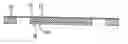
Referring to FIGS. 1A to 1D, they show a conventional laser-marking method for a wafer. Referring to FIG. 1A, firstly, a wafer 10 is provided. The wafer 10 has a first surface 101 and a second surface 102, and a plurality of bumps 103 are disposed on the first surface 101. A glue layer 11 is disposed on the first surface 101. Referring to FIG. 1B, the wafer 10 is ground to be thinner. Referring to FIG. 1C, the glue layer 11 is attached on a first film 12, and a laser light 13 is projected on the second surface 102 of the wafer 10 to mark the wafer 10. Referring to FIG. 1D, finally, the wafer 10 is cut to form a plurality of chips 14.
In the conventional laser-marking method, the first film 12 is not installed on a frame so that the thinned wafer 10 cannot obtain a larger supporting force to support the wafer and the orientation of the laser light 13 cannot be improved. Therefore, the precision for marking the wafer 10 and the quality of products cannot be ensured. In addition, without the frame protection, the thinned wafer 10 is easily broken when the wafer 10 is moved to the printing stage.
Consequently, there is an existing need for providing a laser-marking method for a wafer to solve the above-mentioned problems.
SUMMARY OF THE INVENTIONOne objective of the present invention is to provide a laser-marking method for a wafer. The laser-marking method of the invention comprises the steps of: (a) providing a wafer, the wafer having a first surface and a second surface, and a glue layer disposed on the first surface; (b) attaching the glue layer under a first film, the first film installed on a frame; and (c) projecting a laser light on the second surface of the wafer to mark the wafer.
In the invention, the first film is installed on a frame so that the thinned wafer can obtain a larger supporting force. Therefore, by utilizing the frame, the supporting force is offered and the orientation of the laser can be improved, so that the precision for marking the wafer and the quality of products can be improved. In addition, the thinned wafer is protected from colliding by the frame, so that the wafer can be prevented from breaking when moved to the printing stage.
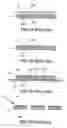
BRIEF DESCRIPTION OF THE DRAWINGSFIGS. 1A to 1D show a conventional laser-marking method for a wafer;
FIGS. 2A to 2G show a laser-marking method for a wafer according to the present invention.
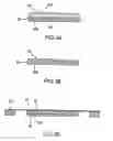
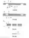
DETAILED DESCRIPTION OF THE INVENTIONReferring to FIGS. 2A to 2G, they show a laser-marking method for a wafer according to the present invention. Referring to FIG. 2A, firstly, a wafer 20 is provided. The wafer 20 has a first surface 201 and a second surface 202, and a plurality of bumps 203 are disposed on the first surface 201. A glue layer 21 is disposed on the first surface 201, and the glue layer 21 is a transparent material. Referring to FIG. 2B, the wafer 20 is ground to be thinner.
Referring to FIG. 2C, the glue layer 21 is attached on a first film 22, and the first film 22 is installed on a frame 23. The shape of the frame 23 matches the shape of the wafer 20. The first film 22 is a transparent material. The frame 23 is used to protect the wafer 20 to prevent breaking. Referring to FIG. 2D, a laser light 24 is projected on the second surface 202 of the wafer 20 to mark the wafer 20, wherein the frame 23 is used to position the laser light 24. The laser light 24 moves co-axially with an image device (not shown) located on the other side of the wafer 20 to proceed the marking step. Before the wafer 20 is marked, at least one positioning point (not shown) is formed on the second surface 202. Referring to FIG. 2E, the wafer 20 and the frame 23 are attached on a second film 25. Referring to FIG. 2F, the frame 23 is removed, and then the wafer 20 is cut to form a plurality of chips 26 by using a laser. Referring to FIG. 2G, finally, the wafer 20 is segregated from the first film 22 and second film 25.
In the invention, the first film 22 is installed on the frame 23 so that the thinned wafer 20 can obtain a larger supporting force. Therefore, by utilizing the frame 23, a supporting force for the wafer 20 is offered and the orientation of the laser light 24 can be improved, so that the precision for marking the wafer 20 and the quality of products can be improve. In addition, the thinned wafer 20 is protected from colliding by the frame 23, so that the wafer 20 can be prevented from breaking when moved to the printing stage.
While the embodiment of the present invention has been illustrated and described, various modifications and improvements can be made by those skilled in the art. The embodiments of the present invention are therefore described in an illustrative but not restrictive sense. It is intended that the present invention may not be limited to the particular forms as illustrated, and that all modifications that maintain the spirit and scope of the present invention are within the scope as defined in the appended claims.
Claims
What is claimed is:1. A laser-marking method for a wafer, the laser-marking method comprising the steps of:
(a) providing a wafer, the wafer having a first surface and a second surface, and a glue layer disposed on the first surface;
(b) attaching the glue layer under a first film, the first film installed on a frame; and
(c) projecting a laser light on the second surface of the wafer to mark the wafer.
2. The method according to claim 1, further comprising a step of attaching the wafer and the frame on a second film after the step (b).
3. The method according to claim 1, wherein the first film is a transparent material.
4. The method according to claim 1, wherein the glue layer is a transparent material.
5. The method according to claim 1, further comprising a step of forming at least one positioning point on the second surface before the step (c).
6. The method according to claim 1, wherein the laser light moves co-axially with an image device located on the other side of the wafer in the step (c).
7. The method according to claim 1, further comprising a step of forming a plurality of chips by cutting the wafer using a laser after the step (c).
8. The method according to claim 1, wherein a plurality of bumps are disposed on the first surface of the wafer.
9. The method according to claim 1, wherein the shape of the frame matches the shape of the wafer.
10. The method according to claim 1, wherein the frame is used to protect the wafer to prevent breaking.
11. The method according to claim 1, wherein the frame is used to position the laser.
12. The method according to claim 1, further comprising a grinding step to thin the wafer after the step (a).
13. The method according to claim 7, further comprising a step of segregating the wafer from the first film and the second film after the step (c).
Images & Drawings included:
Sources:
- United States Patent and Trademark Office - verify current appl. status at the USPTO↗
Similar patent applications:
- » 20100001416
WAFER LASER-MARKING METHOD AND DIE FABRICATED USING THE SAME - » 20090081830
Semiconductor device and method of laser-marking wafers with tape applied to its active surface - » 20110021025
METHOD FOR PRODUCING LASER-MARKED SEMICONDUCTOR WAFER - » 20210375782
Method of producing laser-marked silicon wafer and laser-marked silicon wafer - » 20220331906
Method of printing laser mark and method of producing laser-marked silicon wafer
Recent applications in this class:
- » 20250174573 2025-05-29
PACKAGED SEMICONDUCTOR CHIPS HAVING PROTECTED IDENTIFICATION MARKS THEREIN - » 20250174572 2025-05-29
SEMICONDUCTOR PACKAGE - » 20250174571 2025-05-29
INTERPOSER, METHOD OF FABRICATING THE SAME, AND SEMICONDUCTOR PACKAGE HAVING THE SAME - » 20250167130 2025-05-22
ELECTRONIC DEVICES COMPRISING OVERLAY MARKS - » 20250167129 2025-05-22
METHOD OF MANUFACTURE OVERLAY MARK USING LASER MARKING PROCESS FOR SEMICONDUCTOR DEVICE - » 20250167128 2025-05-22
SEMICONDUCTOR PACKAGE INCLUDING A SOLDER BALL - » 20250157943 2025-05-15
PHOTOLITHOGRAPHY ALIGNMENT PROCESS FOR BONDED WAFERS - » 20250157942 2025-05-15
SEMICONDUCTOR DEVICE - » 20250149464 2025-05-08
SEMICONDUCTOR DEVICE AND METHOD FOR MANUFACTURING THE SAME - » 20250149463 2025-05-08
TOP DIE BACK-SIDE MARKING FOR MEMORY SYSTEMS