Method of improving the stability of a circuit board
US20070111595A1
2007-05-17
11/309,280
2006-07-21
✅ Patent granted
US 7,587,816 B2
2009-09-15
-
-
C. J Arbes
2026-08-03
Abstract:
A printed circuit board includes a mounting hole for receiving a connector pin of either of a first SMC and a second SMC, and a signal line. The signal line is electrically connected to the mounting hole by a conductive layer arranged in and about the mounting hole.
Assignee:
- HON HAI PRECISION INDUSTRY CO., LTD. 624 🇹🇼 Taipei Hsien, Taiwan
- HON HAI PRECISION INDUSTRY CO., LTD. 2,357 🇹🇼 Tu-Cheng, Taipei Hsien, Taiwan
- Hong Fu Jin Precision Industry (Shenzhen) Co., Ltd. 1,915 🇨🇳 Shenzhen, Guangdong Province, China
Interested in similar patents?
Get notified when new applications in this technology area are published.
Classification:
H05K3/005 » CPC main
Apparatus or processes for manufacturing printed circuits; Working of insulating substrates or insulating layers; Mechanical working of the substrate, e.g. drilling or punching Punching of holes
H05K3/005 » CPC main
Apparatus or processes for manufacturing printed circuits; Working of insulating substrates or insulating layers; Mechanical working of the substrate, e.g. drilling or punching Punching of holes
H01R12/57 » CPC further
Structural associations of a plurality of mutually-insulated electrical connecting elements, specially adapted for printed circuits, e.g. printed circuit boards [PCBs], flat or ribbon cables, or like generally planar structures, e.g. terminal strips, terminal blocks; Coupling devices specially adapted for printed circuits, flat or ribbon cables, or like generally planar structures; Terminals specially adapted for contact with, or insertion into, printed circuits, flat or ribbon cables, or like generally planar structures; Fixed connections for rigid printed circuits or like structures characterised by the terminals surface mounting terminals
H05K1/116 » CPC further
Printed circuits; Details; Printed elements for providing electric connections to or between printed circuits; Via connections; Lands around holes or via connections Lands, clearance holes or other lay-out details concerning the surrounding of a via
H05K1/116 » CPC further
Printed circuits; Details; Printed elements for providing electric connections to or between printed circuits; Via connections; Lands around holes or via connections Lands, clearance holes or other lay-out details concerning the surrounding of a via
H05K1/0295 » CPC further
Printed circuits; Details; Programmable, customizable or modifiable circuits adapted for choosing between different types or different locations of mounted components
H05K1/0295 » CPC further
Printed circuits; Details; Programmable, customizable or modifiable circuits adapted for choosing between different types or different locations of mounted components
H05K2201/0382 » CPC further
Indexing scheme relating to printed circuits covered by; Conductive materials; Structure of the conductor; Conductor shape Continuously deformed conductors
H05K2201/0382 » CPC further
Indexing scheme relating to printed circuits covered by; Conductive materials; Structure of the conductor; Conductor shape Continuously deformed conductors
H05K2201/09954 » CPC further
Indexing scheme relating to printed circuits covered by; Shape and layout; Shape or layout details not covered by a single group of - More mounting possibilities, e.g. on same place of PCB, or by using different sets of edge pads
H05K2201/09954 » CPC further
Indexing scheme relating to printed circuits covered by; Shape and layout; Shape or layout details not covered by a single group of - More mounting possibilities, e.g. on same place of PCB, or by using different sets of edge pads
H05K2201/10189 » CPC further
Indexing scheme relating to printed circuits covered by; Details of components or other objects attached to or integrated in a printed circuit board; Types of components Non-printed connector
H05K2201/10189 » CPC further
Indexing scheme relating to printed circuits covered by; Details of components or other objects attached to or integrated in a printed circuit board; Types of components Non-printed connector
H05K2203/1476 » CPC further
Indexing scheme relating to apparatus or processes for manufacturing printed circuits covered by; Related to the order of processing steps Same or similar kind of process performed in phases, e.g. coarse patterning followed by fine patterning
H05K2203/1476 » CPC further
Indexing scheme relating to apparatus or processes for manufacturing printed circuits covered by; Related to the order of processing steps Same or similar kind of process performed in phases, e.g. coarse patterning followed by fine patterning
Y10T29/49117 » CPC further
Metal working; Method of mechanical manufacture; Electrical device making Conductor or circuit manufacturing
Y10T29/49126 » CPC further
Metal working; Method of mechanical manufacture; Electrical device making; Conductor or circuit manufacturing; On flat or curved insulated base, e.g., printed circuit, etc. Assembling bases
Y10T29/4913 » CPC further
Metal working; Method of mechanical manufacture; Electrical device making; Conductor or circuit manufacturing; On flat or curved insulated base, e.g., printed circuit, etc. Assembling to base an electrical component, e.g., capacitor, etc.
Y10T29/49144 » CPC further
Metal working; Method of mechanical manufacture; Electrical device making; Conductor or circuit manufacturing; On flat or curved insulated base, e.g., printed circuit, etc.; Assembling to base an electrical component, e.g., capacitor, etc. by metal fusion
Y10T29/49165 » CPC further
Metal working; Method of mechanical manufacture; Electrical device making; Conductor or circuit manufacturing; On flat or curved insulated base, e.g., printed circuit, etc.; Manufacturing circuit on or in base by forming conductive walled aperture in base
H01R13/60 IPC
Details of coupling devices of the kinds covered by groups or - Means for supporting coupling part when not engaged
H01K3/10 IPC
Apparatus or processes adapted to the manufacture, installing, removal, or maintenance of incandescent lamps or parts thereof; Manufacture of mounts or stems Machines therefor
Description
FIELD OF THE INVENTIONThe present invention relates to a printed circuit board (PCB), and more particularly to a layout for mounting holes of a PCB.
DESCRIPTION OF RELATED ARTIn general, surface mounted components (SMCs), including resistors, capacitors, inductors and so on, are mounted to a PCB by mounting holes. The mounting holes are arranged on the PCB in a matched relationship with connector pins of the SMCs. The mounting holes have different configurations due to varied configurations of the connector pins of the SMCs.
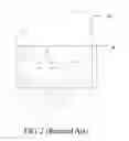
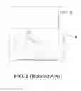
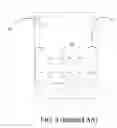
For example, two common SMCs are Universal Serial Bus (USB) port and Institute of Electrical and Electronics Engineers (IEEE) 1394 port. In designing a layout of a PCB it is common to include mounting holes for both USB and IEEE ports even though only one will be used at any given time. In Laying out a configuration for mounting holes of a PCB for mounting the USB port or the IEEE 1394 port, computer software such as Protel is used. Referring to FIGS. 2 to 4, typical configurations for mounting holes of the ports are designed and prepared in computerized layouts of a PCB. An area A that is part of a situation area 10 (FIG.2) of the PCB for locating mounting holes of the IEEE 1394 port is similar to an area B that is part of a situation area 20 (FIG.3) of the PCB for locating mounting holes of the USB port. For instance, the mounting hole 12 of the IEEE 1394 port is the same as the mounting hole 22 of the USB port. Therefore, when designing a layout of the PCB, the corresponding areas A and B may be superimposed to save space on the PCB (FIG.4).
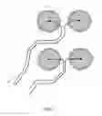
Referring to FIG. 5, in the design process, a centering point O1 of the mounting hole 12 for the IEEE 1394 port is supposed to be exactly aligned with the corresponding centering point O2 of the mounting hole 22 for the USB port. A signal line 40 is connected to the aligned centering points O1, O2 to complete the electrical connections of the two ports when needed. However, it is difficult in the manufacturing process to ensure the centering points O1, O2 are exactly aligned because of errors of design and manufacturing tools. Therefore, when the mounting holes are punched, misalignment in the centering holes will result in a misshapen mounting hole which may cause a gap between the mounting pin of a port and the signal line 40 resulting in an open circuit.
What is desired, therefore, is a PCB having mounting holes that can work normally even when a misalignment of centering holes occurs.
SUMMARY OF THE INVENTIONIn one preferred embodiment, a PCB includes a mounting hole for receiving a connector pin of either of a first SMC and a second SMC, and a signal line. The signal line is electrically connected to the mounting hole by a conductive layer arranged in and about the mounting hole.
Other advantages and novel features will become more apparent from the following detailed description of preferred embodiments when taken in conjunction with the accompanying drawings, in which:
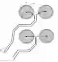
BRIEF DESCRIPTION OF THE DRAWINGSFIG. 1 is a schematic view of a computer generated layout of four mounting holes with conductive layers marked for punching with centering holes for fixing either one of an IEEE 1394 port and USB port of a PCB in accordance with a preferred embodiment of the present invention;
FIG. 2 is a schematic view of a computer generated layout of an area with mounting holes for fixing an IEEE 1394 port of a typical PCB;
FIG. 3 is a schematic view of a computer generated layout of an area with mounting holes for fixing a USB port of a typical PCB;
FIG. 4 is a schematic view of a computer generated layout combining the areas of FIG. 2 and FIG. 3 with mounting holes for fixing either one of IEEE 1394 port of FIG. 1 and USB port of FIG. 2 of a typical PCB; and
FIG. 5 is a schematic view of a computer generated layout of four mounting holes of FIG. 4 marked for punching with centering holes.
DETAILED DESCRIPTION OF THE INVENTIONIn a preferred embodiment of the present invention, a conventional layout for mounting holes (not labeled) of a circuit assembly like a printed circuit board (PCB) as shown in FIG. 4 is used, wherein a configuration of mounting holes for one surface mounted component (SMC) such as an Institute of Electrical and Electronics Engineers (IEEE) 1394 port is superimposed over a configuration of mounting holes for another SMC such as a Universal Serial Bus (USB) port. The configurations are superimposed in such way as to align as many of the mounting holes of both SMCs as possible for common use by pins of both SMCs. Then, as shown in detail in FIG. 1, a conductive layer (such as a copper foil) 58, having a generally circular shape is formed over each of the common mounting holes. A radius of each of the conductive layers is greater than a radius of the mounting holes thereunder to allow for any misalignment of centering points A1, A2. The centering points Al, A2 are for alignment of a punch apparatus during manufacturing of the PCB. Al marks a center point for a mounting hole for the 1394 port and A2 marks a center point for a mounting hole for the USB port. Signal lines 56 are formed on the PCB each terminating at a center of a corresponding conductive layer 58.
During a process of punching holes in the PCB according to the layout described above, first one set of mounting holes is punched corresponding to the configuration for the 1394 port then another set of mounting holes is punched corresponding to the configuration for the USB port. The common holes will then have been punched twice, once for each set. When the common holes with the conducting layers 58 are punched, the conducting layers 58 do not punch cleanly. That is to say as the holes are punched in the PCB, the area of the conducting layers 58 pierced by the punching apparatus curls down and flattens against an upper portion of a circular sidewall defining each of the common mounting holes. Thus, even if a common mounting hole is misshapen due to misalignment of the two punches, a pin of the 1394 port or of the USB port received in the mounting hole will still form a closed circuit via the conductive layer lining the mounting hole with the signal line 56.
It is believed that the present embodiment and its advantages will be understood from the foregoing description, and it will be apparent that various changes may be made thereto without departing from the spirit and scope of the invention or sacrificing all of its material advantages, the example hereinbefore described merely being a preferred or exemplary embodiment.
Claims
What is claimed is:1. A printed circuit board comprising:
a mounting hole receiving a connector pin of either of a first surface mounted component or a second surface mounted component;
a signal line electrically connected to the mounting hole; and
a conductive layer arranged in and about the mounting hole.
2. The printed circuit board as claimed in claim 1, wherein the mounting hole runs through the printed circuit board when being punched.
3. The printed circuit board as claimed in claim 2, wherein the signal line is electrically connected to the mounting hole by the conductive layer.
4. The printed circuit board as claimed in claim 3, wherein the conductive layer is copper foil.
5. A method for improving stability of a circuit board, comprising the steps of:
arranging a first configuration of at least one mounting hole for a first surface mounted component on the circuit board;
arranging a second configuration of at least another mounting hole for a second surface mounted component on the circuit board, the first configuration superimposed over the second configuration;
setting a signal line being connected to the first configuration and the second configuration; and
arranging a conductive layer arranged in and about the mounting hole.
6. The method as claimed in claim 5, further comprising the step of punching the at least one mounting hole for the first surface mounted component corresponding to the first configuration.
7. The method as claimed in claim 6, further comprising the step of punching the at least another mounting hole for the second surface mounted component corresponding to the second configuration.
8. The method as claimed in claim 7, wherein the conductor layer is copper foil.
9. A method for improving stability of a circuit assembly, comprising the steps of:
forming a first mounting hole in said circuit assembly for electrical connection of said circuit assembly with a first component via said first mounting hole;
forming a second mounting hole in said circuit assembly for electrical connection of said circuit assembly with a second component via said second mounting hole by means of superimposing substantially said second mounting hole over said first mounting hole; and placing a conductive layer over said superimposed first and second mounting holes to complement any configuration difference between said first and second mounting holes so as to enhance said electrical connection of said circuit assembly with a selective one of said first and second components via said first and second mounting holes correspondingly.
10. The method as claimed in claim 9, wherein said placing step comprises the step of covering said superimposed first and second mounting holes commonly with said conductive layer and the step of punching said covering conductive layer to deform said conductive layer for complementing of said configuration difference.
Images & Drawings included:
Sources:
- United States Patent and Trademark Office - verify current appl. status at the USPTO↗
Recent applications in this class:
- » 20200344887 2020-10-29
System for fastening multiple stacked planar objects with adaptive compensatory mechanism - » 20200100366 2020-03-26
Method of producing an electrical through connection between opposite surfaces of a flexible substrate - » 20140202747 2014-07-24
CIRCUIT BOARD AND MANUFACTURING METHOD THEREOF - » 20140053397 2014-02-27
Method for manufacturing printed circuit board - » 20080282864 2008-11-20
Punch device with interchangeable punch and variable punch pattern - » 20080023817 2008-01-31
Component packaging apparatus, systems, and methods - » 20050158455 2005-07-21
Method of producing multilayer interconnection board - » 20050123860 2005-06-09
Dielectric with fluorescent material - » 20050116387 2005-06-02
Component packaging apparatus, systems, and methods - » 20050116299 2005-06-02
Component packaging apparatus, systems, and methods
Recent applications for this Assignee:
- » 20120329427 2012-12-27
Wireless unlocking system - » 20120304477 2012-12-06
Counterbore hole chamfer depth measuring apparatus and method - » 20120276769 2012-11-01
Connector retaining device - » 20120270418 2012-10-25
Printed circuit board used in server - » 20120262041 2012-10-18
Electronic device enclosure - » 20120251746 2012-10-04
Device housing and method for making the same - » 20120236486 2012-09-20
Power supply - » 20120231659 2012-09-13
Connector assembly - » 20120220174 2012-08-30
Cable clamp having a base with a tapered hole and a sleeve with a tapered outer wall to clamp a cable in-between - » 20120194117 2012-08-02
Fan control system