Embedded system
US20070174495A1
2007-07-26
11/539,209
2006-10-06
✅ Patent granted
US 7,602,655 B2
2009-10-13
-
-
Tuan T Nguyen | Hien N Nguyen
2027-07-19
Abstract:
An embedded system, comprising a programmable device, a micro controller and an I/O interface is disclosed. The programmable device consists of a pin set for signal delivery. The micro controller device controls the programmable device via the pin set. The I/O interface receives a program code provided externally. The micro controller executes a command sequence to program the program code into the programmable device via the pin set, and the programmable device uses the program code to provide the specific function. The command sequence may also be provided externally and sent to the micro controller via the well-known general I/O interface.
Inventors:
- You-Wen Chang 8 🇹🇼 Hsinchu City, Taiwan
- Chien-Hsun Tung 6 🇹🇼 Taichung City, Taiwan
- Li-Lien Lin 10 🇹🇼 Hsinchu, Taiwan
- You-Wen Chang 5 🇹🇼 Hsinchu, Taiwan
- Chien-Hsun Tung 4 🇹🇼 Taichung, Taiwan
Assignee:
- MEDIATEK INC. 3,761 🇹🇼 Hsin-Chu, Taiwan
Interested in similar patents?
Get notified when new applications in this technology area are published.
Classification:
G11C17/18 » CPC main
Read-only memories programmable only once; Semi-permanent stores, e.g. manually-replaceable information cards in which contents are determined by selectively establishing, breaking or modifying connecting links by permanently altering the state of coupling elements, e.g. PROM Auxiliary circuits, e.g. for writing into memory
G06F7/725 » CPC further
Methods or arrangements for processing data by operating upon the order or content of the data handled; Methods or arrangements for performing computations using a digital non-denominational number representation, i.e. number representation without radix; Computing devices using combinations of denominational and non-denominational quantity representations, e.g. using difunction pulse trains, STEELE computers, phase computers using residue arithmetic; Finite field arithmetic over elliptic curves
G06F21/57 » CPC further
Security arrangements for protecting computers, components thereof, programs or data against unauthorised activity; Monitoring users, programs or devices to maintain the integrity of platforms, e.g. of processors, firmware or operating systems Certifying or maintaining trusted computer platforms, e.g. secure boots or power-downs, version controls, system software checks, secure updates or assessing vulnerabilities
G11C7/24 » CPC further
Arrangements for writing information into, or reading information out from, a digital store Memory cell safety or protection circuits, e.g. arrangements for preventing inadvertent reading or writing; Status cells; Test cells
H04L9/3066 » CPC further
arrangements for secret or secure communications Cryptographic mechanisms or cryptographic ; Network security protocols; Public key, i.e. encryption algorithm being computationally infeasible to invert or user's encryption keys not requiring secrecy involving algebraic varieties, e.g. elliptic or hyper-elliptic curves
G11B20/00086 » CPC further
Signal processing not specific to the method of recording or reproducing; Circuits therefor Circuits for prevention of unauthorised reproduction or copying, e.g. piracy
G11B2220/213 » CPC further
Record carriers by type; Disc-shaped record carriers characterised in that the disc is of read-only, rewritable, or recordable type Read-only discs
G11B2220/2562 » CPC further
Record carriers by type; Disc-shaped record carriers characterised in that the disc is based on a specific recording technology; Optical discs DVDs [digital versatile discs]; Digital video discs; MMCDs; HDCDs
H04L2209/12 » CPC further
Additional information or applications relating to cryptographic mechanisms or cryptographic arrangements for secret or secure communication Details relating to cryptographic hardware or logic circuitry
G06F3/00 IPC
Input arrangements for transferring data to be processed into a form capable of being handled by the computer; Output arrangements for transferring data from processing unit to output unit, e.g. interface arrangements
G11C7/00 IPC
Arrangements for writing information into, or reading information out from, a digital store
Description
BACKGROUND OF THE INVENTION
1. Field of the Invention
The invention relates to DVD-ROMs, and more particularly, to programming a device with a reduced number of pins in an embedded system.
2. Description of the Related Art
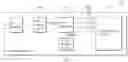
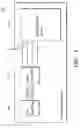
FIG. 1 shows a conventional embedded system 100 with an externally coupled program provider 110. The embedded system 100 may be part of a DVD-ROM storing copyright information, or part of a general purpose digital device executing various applications programmed therein. The embedded system 100 typically comprises a program controller 120 and a programmable device 130. The program controller 120 accesses the programmable device 130 via a plurality of pins 105. The definition of each pin 105 is dependent on the type of device 130. When the programmable device 130 needs to be programmed with a specific application, a program code #DATA corresponding to the application is provided externally through a program provider 110. Conventionally, additional control pins such as 107 and 109 are required to perform the programming, through which the program provider 110 directly connects to the programmable device 130. One or more multiplexers 103 may be implemented on each pin 105, selecting signals from the program provider 110 or program controller 120 as an input to the programmable device 130. When programming, the multiplexers 103 select signals delivered via the control pins 107 to program the programmable device 130, while some additional signals are directly sent via the control pins 109. In some cases, the program provider 110 directly connects the program controller 120 by a bus 101, and the program controller 120 may comprise a level shifter (not shown) to map signals delivered via the bus 101 to each pin 105. The control pins 107 and 109 are still indispensable in the conventional architecture. There may be various types of programmable device 130, each conforming to different pin standards, and the program provider 110 performs the programming by executing a command sequence #CMD specifically designed for the programmable device. The layout of the control pins 105, 107 and 109 are also type dependent, as well as the signal protocol used by the program provider 110 and program controller 120. This architecture is deemed inflexible because the program provider 110, program controller 120 and corresponding pins can not provide compatibility when the programmable device 130 needs upgrade. Thus, a flexible architecture is desirable.
BRIEF SUMMARY OF THE INVENTION
An exemplary embodiment of an embedded system comprises a programmable device, a micro controller and an I/O interface. The programmable device consists of a pin set for signal delivery. The micro controller device controls the programmable device via the pin set. The I/O interface receives an externally provided program code. The micro controller executes a command sequence to program the program code into the programmable device via the pin set, and the programmable device executes the program code to provide the specific function. The command sequence may also be provided externally and sent to the micro controller via the I/O interface.
The embedded system may further comprise a first memory device coupled to the I/O interface and micro controller. The program code is received from the I/O interface and stored in the first memory device. When programming the programmable device, the micro controller reads the program code from the first memory device and writes to the programmable device. The command sequence is also stored in the first memory device when provided. When programming the programmable device, the micro controller reads the command sequence from the first memory device and executes it to perform the programming. The first memory device is a volatile memory device or a DRAM.
Alternatively, the embedded system further comprises a second memory device coupled to the micro controller, storing the command sequence; wherein when programming the programmable device, the micro controller reads the command sequence from the second memory device and executes it to perform the programming. The second memory device is a nonvolatile memory device, a FLASH or an EEPROM.
The embedded system may be a DVD-ROM. The programmable device is an e-fuse or a one time programmable chip that can only be programmed once or re-programmable device that can be programmed many times. The program code comprises confidential information to be protected, and the specific function is storage of the confidential information modification of which is disallowed. The I/O interface is an IDE interface, a SATA interface or a well-known general interface. A detailed description is given in the following embodiments with reference to the accompanying drawings.
BRIEF DESCRIPTION OF THE DRAWINGS
The invention can be more fully understood by reading the subsequent detailed description and examples with references made to the accompanying drawings, wherein:
FIG. 1 shows a conventional embedded system 100 with an externally coupled program provider 110;
FIGS. 2, 3 and 4 show embodiments of embedded system according to the disclosure.
DETAILED DESCRIPTION OF THE INVENTION
The following description is of the best-contemplated mode of carrying out the invention. This description is made for the purpose of illustrating the general principles of the invention and should not be taken in a limiting sense. The scope of the invention is best determined by reference to the appended claims.
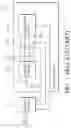
FIG. 2 shows an embodiment of an embedded system 200. A micro controller 210 is provided, dedicated to controlling programmable device 130 over a plurality of pins 105. In this way, no additional pins such as 107 and 109 are required to program the programmable device 130. Furthermore, the command sequence #CMD executed by the micro controller 210 is replaceable, thus, when the programmable device 130 is upgraded to a different type, the micro controller 210 can still perform the programming by executing a corresponding command sequence #CMD of the type. In the embedded system 200, the programmable device 130 performs program defined functions. For example, the programmable device 130 may be a one time programmable device for storage of copyright information or confidential information that modifications thereof are permanently disallowed. The programmable device 130 is directly connected to the micro controller 210 by a set of pins 105. The pins 105 may be type dependent, thus detailed signal description of each pin is not described herein. The micro controller 210 may comprise a lookup table flexibly defining protocols of each pin 105 according to the type of programmable device 130, thus when the programmable device 130 is upgraded, the micro controller 210 can still adapt to it without being outdated. In the embedded system 200, an I/O interface 206 is coupled to the micro controller 210, receiving a program code #DATA provided externally. The program code #DATA may be a sequence of instructions executable for the programmable device 130, or a data block to be stored in the programmable device 130. In a programming procedure, the micro controller 210 executes the command sequence #CMD to program the program code #DATA into the programmable device 130 via the pins 105, such that the specific function can be served by the programmable device 130 with the program code #DATA.
In FIG. 2, the command sequence #CMD is stored in a second memory device 204 as a firmware. The second memory device 204, for example, may be a nonvolatile memory device such as a FLASH or an EEPROM. A first memory device 202 coupled to the I/O interface 206 and micro controller 210, may be a volatile memory device such as a DRAM. When the I/O interface 206 receives the program code #DATA, it is temporally stored in the first memory device 202. When the programming procedure begins, the micro controller 210 executes the command sequence #CMD stored in the second memory device 204, and in response, the program code #DATA in the first memory device 202 is read and written to the programmable device 130 by the micro controller 210.
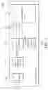
FIG. 3 shows an embodiment of an embedded system 300. The embedded system 300 does not comprise the second memory device 204. Thus, the command sequence #CMD is also provided externally via the I/O interface 206 and stored in the first memory device 202. When the programming procedure begins, the micro controller 210 reads the command sequence #CMD from the first memory device 202 and executes it to perform the programming.
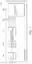
FIG. 4 shows an embodiment of an embedded system 400. The embedded system 400 further excludes the first memory device 202 as shown in FIG. 3. The micro controller 210 is directly triggered to perform a programming procedure upon receipt of the command sequence #CMD and program code #DATA. If the embedded system 200 is a DVD-ROM, the programmable device 130 may be an e-fuse or a one time programmable chip that can only be programmed once, and the program code #DATA is the confidential information to be protected. When the programmable device 130 is programmed with the confidential information, modification thereof is unallowable and the copyright is protected. As an example, the I/O interface 206 may be an IDE interface, a SATA interface or a network interface. In this way, the program code #DATA can be flexibly provided from various sources such as the Internet or portable devices.
The disclosure provides a simplified architecture with more compatibility and flexibility for programmable devices. While the invention has been described by way of example and in terms of preferred embodiment, it is to be understood that the invention is not limited thereto. To the contrary, it is intended to cover various modifications and similar arrangements (as would be apparent to those skilled in the art). Therefore, the scope of the appended claims should be accorded the broadest interpretation so as to encompass all such modifications and similar arrangements.
Claims
What is claimed is:1. An embedded system, comprising:
a programmable device, storing program codes, consisting of a pin set for signal delivery,
a micro controller, connected to the programmable device, controlling the programmable device via the pin set;
an I/O interface, coupled to the micro controller, receiving a program code provided externally, in which a specific function is defined; wherein:
the micro controller executes a command sequence to program the program code into the programmable device via the pin set; and
the programmable device executes the programmed program code to provide the specific function.
2. The embedded system as claimed in claim 1, wherein the command sequence is provided externally and sent to the micro controller via the I/O interface.
3. The embedded system as claimed in claim 1, further comprising a first memory device coupled to the I/O interface and micro controller; wherein:
the program code is received from the I/O interface and stored in the first memory device; and
when programming the programmable device, the micro controller reads the program code from the first memory device and writes to the programmable device.
4. The embedded system as claimed in claim 3, wherein:
the command sequence is provided externally via the I/O interface and stored in the first memory device; and
when programming the programmable device, the micro controller reads the command sequence from the first memory device and executes it to perform the programming.
5. The embedded system as claimed in claim 3, wherein the first memory device is a volatile memory device or a DRAM.
6. The embedded system as claimed in claim 3, further comprising a second memory device coupled to the micro controller, storing the command sequence; wherein when programming the programmable device, the micro controller reads the command sequence from the second memory device and executes it to perform the programming.
7. The embedded system as claimed in claim 6, wherein the second memory device is a nonvolatile memory device, a FLASH or an EEPROM.
8. The embedded system as claimed in claim 1, wherein the embedded system is an optical storage device.
9. The embedded system as claimed in claim 8, wherein:
the programmable device is an e-fuse or a one time programmable chip that can only be programmed once;
the program code comprises confidential information to be protected; and
the specific function is storage of the confidential information of which modification is unallowable.
10. The embedded system as claimed in claim 1, wherein the I/O interface is an IDE interface, a SATA interface or a network interface.
Images & Drawings included:
Sources:
- United States Patent and Trademark Office - verify current appl. status at the USPTO↗
Similar patent applications:
- » 20120303946
Device for reprogramming an embedded system to allow the system to return to an initial embedded system information or a reprogrammed embedded system information - » 20190227858
Embedded system, embedded system control method and data consistency judgment method - » 20210350003
Securing boot controller for an embedded system, associated embedded system and securing boot method - » 20200089482
Method for installing a program on an embedded system, an embedded system for such a method, and a method for generating additional information - » 20250278311
EMBEDDED SYSTEM RUNNING METHOD AND APPARATUS, AND EMBEDDED SYSTEM AND CHIP - » 20240370553
EMBEDDED SYSTEM STARTUP METHOD, STARTUP PROGRAM, AND EMBEDDED SYSTEM - » 20250278312
EMBEDDED SYSTEM RUNNING METHOD AND APPARATUS, AND EMBEDDED SYSTEM AND CHIP - » 20240362083
Embedded system running method and apparatus, and embedded system and chip - » 20220012046
OS-INDEPENDENT PERIPHERAL PLUG-AND-PLAY AND DRIVER UPDATE METHOD FOR EMBEDDED SYSTEMS AND FIRMWARE DATA TRANSMISSION METHOD FOR EMBEDDED SYSTEM PLATFORM - » 20130013756
NETWORK UNIT REPLACING METHOD FOR EMBEDDED SYSTEM DEVICE HAVING INTERNAL NETWORK UNIT AND EMBEDDED SYSTEM DEVICE
Recent applications in this class:
- » 20250285694 2025-09-11
MEMORY DEVICE AND OPERATING METHOD OF THE SAME - » 20250285693 2025-09-11
EMBEDDED ELECTRONIC FUSES - » 20250266114 2025-08-21
METHODS AND APPARATUS TO DELETE AND PREVENT RECOVERY OF DATA STORED IN A MEMORY ARRAY - » 20250201321 2025-06-19
VERTICAL FUSE MEMORY IN ONE-TIME PROGRAM MEMORY CELLS - » 20250191667 2025-06-12
MEMORY CIRCUIT AND METHOD OF OPERATING SAME - » 20250149101 2025-05-08
VOLTAGE REGULATION FOR MEMORY ARRAY TEST PROCEDURES - » 20250131967 2025-04-24
MEMORY DEVICE AND METHOD FOR OPERATING THE SAME - » 20250124993 2025-04-17
NON-VOLATILE MEMORY DEVICE INCLUDING SENSE AMPLIFIER AND METHOD FOR OPERATING THE SAME - » 20250104785 2025-03-27
NON-VOLATILE MEMORY CIRCUIT AND METHOD - » 20250095761 2025-03-20
HIGH VOLTAGE TRANSFER DEVICE AND A MEMORY DEVICE INCLUDING THE SAME
Recent applications for this Assignee:
- » 20250274873 2025-08-28
METHOD AND APPARATUS OF PERFORMING POWER CONTROL ON WIRELESS COMMUNICATION DEVICE WITH POWER ESTIMATION CALIBRATION AND RELATED WIRELESS COMMUNICATION DEVICE - » 20250274501 2025-08-28
VIDEO TRANSMISSION METHOD THROUGH DYNAMIC DISPATCHING MPDUS AMONG MULTI-LINKS - » 20250266617 2025-08-21
ANTENNA INCLUDING CONDUCTIVE PLATES AND CONDUCTIVE LOOPS AND CAPABLE OF REDUCING SPURIOUS EMISSIONS - » 20250247505 2025-07-31
IMAGE PROCESSING SYSTEM AND IMAGE PROCESSING METHOD - » 20250233905 2025-07-17
Multimedia System with Dynamic Adaptation - » 20250233593 2025-07-17
Counter System and Method of Driving the Counter System with Zero Accumulated Error - » 20250227077 2025-07-10
Router-Bridge Capable of Fast Exchanging Network Packets - » 20250225301 2025-07-10
METHOD FOR PERFORMING BLOCK LEVEL EXPLORATION OF INTEGRATED CIRCUIT DESIGN, ASSOCIATED ELECTRONIC DEVICE AND ASSOCIATED COMPUTER-READABLE MEDIUM - » 20250224888 2025-07-10
APPARATUS AND METHOD FOR HANDLING SUDDEN POWER LOSS OF STORAGE DEVICE - » 20250224442 2025-07-10
Dynamic Voltage Stress Condition Optimization Method and Dynamic Voltage Stress Condition Optimization System Capable of Performing Block-based Dynamic Voltage Stress Wafer Testing Process