Dicing method using an encased dicing blade submerged in cooling water
US20070175466A1
2007-08-02
11/699,794
2007-01-30
✅ Patent granted
US 7,557,016 B2
2009-07-07
-
-
Hsien-ming Lee | Walter H Swanson
2027-01-30
Abstract:
A dicing blade (2) which rotates at high speed is surrounded by a case (3). A semiconductor wafer (1) is cut by a dicing device in which the case is filled with a cooling water (4). The case (3) is provided with a cooling water nozzle (8) for continuously supplying the cooling water and a gap (10) for discharging the cooling water out of the case. By adjusting a supply rate and a discharge rate of the cooling water, a proper water pressure can be applied to an inside of the case, thereby making it possible to cool the dicing blade and the cutting point with efficiency. As a result, it is possible to suppress chipping and cracking of the semiconductor device due to lack of cooling.
Assignee:
- Seiko Instruments Inc. 772 🇯🇵 , Japan
Interested in similar patents?
Get notified when new applications in this technology area are published.
Classification:
H01L21/78 IPC
Processes or apparatus adapted for the manufacture or treatment of semiconductor or solid state devices or of parts thereof; Manufacture or treatment of devices consisting of a plurality of solid state components formed in or on a common substrate or of parts thereof; Manufacture of integrated circuit devices or of parts thereof; Manufacture or treatment of devices consisting of a plurality of solid state components or integrated circuits formed in, or on, a common substrate with subsequent division of the substrate into plural individual devices
B28D5/0076 » CPC main
Fine working of gems, jewels, crystals, e.g. of semiconductor material; apparatus or devices therefor; Accessories specially adapted for use with machines for fine working of gems, jewels, crystals, e.g. of semiconductor material for removing dust, e.g. by spraying liquids; for lubricating, cooling or cleaning tool or work
B28D1/04 IPC
Working stone or stone-like materials, e.g. brick, concrete or glass , not provided for elsewhere; Machines, devices, tools therefor by sawing with circular or cylindrical saw-blades or saw-discs
Description
BACKGROUND OF THE INVENTION
1. Field of the Invention
The present invention relates to a dicing machine and method enabling reduction of chipping and cracking both of which are caused during dicing a semiconductor wafer.
2. Description of the Related Art
Conventionally, a semiconductor device having a circuit formed on a semiconductor wafer is generally subjected to dicing using a dicing blade which rotates at high speed. However, in this method, heat generates when cutting the wafer by using the dicing blade, so during the dicing, the cutting is performed while supplying cooling water to a cutting portion to suppress the heat generation.
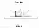
In the following, an example of a conventional dicing method will be described with reference to the drawings. FIG. 5 shows a conventional dicing method, and is a side view of a main portion of a dicing device. There are provided a semiconductor wafer 1, a dicing blade 2, a cooling water 4, a dicing tape 5, and a cooling water nozzle 8. The dicing blade 2 rotates at several tens of thousands rpm to cut the semiconductor wafer 1 which is an object to be machined. At this time, in order to eliminate the heat generated during the cutting, the wafer is cut while supplying the cooling water 4 to the blade. However, the cooling water is flung away from the rotating dicing blade due to a centrifugal force. Therefore, it is difficult to supply a sufficient amount of water to a cutting point. Thus, there is a problem in that chipping is caused in an end surface of the semiconductor device (semiconductor chip) after the dicing.
In order to solve the problem, there has been developed various dicing methods.
For example, JP 06-85054A discloses a technique of suppressing ruptures, chipping, and cracking caused at the time of dicing the wafer by providing a mechanism including a porous blade used as a dicing blade, for emitting pure water or air from an inside of the blade, to thereby prevent clogging of the blade.
JP 06-5700 A discloses a dicing method in which the dicing blade is sandwiched from both sides thereof by flanges, and pure water is ejected from gaps between the dicing blade and the flanges. However, in this method, the cooling water is directly supplied to the cutting point, so an excessive force is exerted on the semiconductor chip, with the result that flapping is caused, and chipping occurs.
JP 2000-349046 A discloses a method of supplying the cooling water in which a force to be applied to the semiconductor chip is devised to reduce the chipping.
JP 06-13460 A discloses a dicing method in which the cooling water nozzle is provided not only in the vicinity of the cutting portion but also on a blade outer peripheral surface, thereby elongating a life of the blade and keeping the chipping to a minimum.
SUMMARY OF THE INVENTION
As described above, for dicing the semiconductor device, there has been developed various methods of supplying the cooling water to the dicing blade in order to suppress heat generation of the dicing blade. However, those developments are not sufficient, so there are still caused chipping and cracking in the semiconductor device. It is therefore an object of the present invention to solve the above-mentioned problem.
In order to achieve the above-mentioned object, there is provided the following means. That is, (1) a dicing method characterized in that, in order to reliably supply a cooling water required for dicing a semiconductor wafer to a cutting portion, a dicing blade is surrounded by a case and an inside of the case is filled with the cooling water, thereby being capable of positively supplying water to the cutting portion at a time of dicing and of reducing chipping of the semiconductor device generated at the time of dicing; (2) a dicing method characterized in that a cooling water nozzle capable of continuously supplying the cooling water is attached to the case surrounding the dicing blade, and by enabling adjustment of a flow rate, a proper water pressure in the case can be ensured, thereby making it possible to sufficiently supply the cooling water to a cutting point; (3) a dicing method characterized in that a gap is formed between the case and the semiconductor wafer, and based on a gap size, a discharge rate of the cooling water to the outside of the case can be adjusted; (4) a dicing method characterized in that a brush is provided in the gap between the case and the semiconductor wafer, thereby reducing the discharge rate of the cooling water to ensure the proper water pressure in the case; (5) a dicing device, for cutting a semiconductor wafer with a dicing blade which rotates at high speed, characterized by including: the dicing blade; and a case surrounding the dicing blade and maintaining a gap between the semiconductor wafer and the case; and (6) a dicing device, for cutting a semiconductor wafer with a dicing blade which rotates at high speed, characterized by including: the dicing blade; a case surrounding the dicing blade and maintaining a gap between the semiconductor wafer and the case; and a brush provided in the gap.
According to the present invention, the cooling water can be sufficiently supplied over an entire dicing blade during cutting of the wafer, so the blade can be sufficiently cooled. Therefore, it is possible to achieve dicing which causes few numbers of chipping and cracking in the semiconductor device on the semiconductor chip. That is, a high-quality semiconductor device can be supplied in a stable manner.
BRIEF DESCRIPTION OF THE DRAWINGS
In the accompanying drawings:
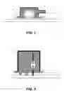
FIG. 1 is a blade side view showing a dicing method according to a first embodiment of the present invention;
FIG. 2 is a blade front view showing the dicing method according to the first embodiment of the present invention;
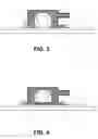
FIG. 3 is a blade side view showing a dicing method according to a second embodiment of the present invention;
FIG. 4 is a blade side view showing a dicing method according to a third embodiment of the present invention; and
FIG. 5 is a blade side view showing a conventional dicing method.
DETAILED DESCRIPTION OF THE PREFERRED EMBODIMENTS
Hereinafter, preferred embodiments of the present invention will be described with reference to the drawings.
Embodiment 1
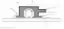
A dicing method according to a first embodiment of the present invention will be described with reference to FIGS. 1 and 2. FIG. 1 is a side view of a dicing device main portion including a dicing blade. FIG. 2 is a front view of the main portion. A semiconductor wafer 1 is bonded to a dicing tape 5 and is held on a wafer stage portion (not shown) of the dicing device. The semiconductor wafer 1 which is held is cut due to a rotation 9 of a dicing blade 2, to thereby provide individual semiconductor chips 6. The dicing blade is surrounded by a case 3 filled with a cooling water 4 and is submerged in the cooling water 4. In FIGS. 1 and 2, the case 3 surrounds the dicing blade 2 with five flat surfaces of the case 3, including an upper surface, two front surfaces, and two side surfaces. As long as only a surface facing the semiconductor wafer is opened, the case may have a spherical surface. The cooling water 4 in the case 3 is supplied from a cooling water nozzle 8 and passes through the case 3 to be used for cooling the dicing blade 2 and a cutting point 7. After that, the cooling water 4 is discharged from a gap 10 between the semiconductor wafer 1 and the case 3 to an outside of the case 3 together with cutting powder. By adjusting an amount of water continuously supplied from the cooling water nozzle 8 into the case 3, a proper pressure is applied to an inside of the case 3, thereby sufficiently supplying the cooling water to the cutting point and the vicinity thereof. As a result, lack of cooling at the cutting point which has conventionally been the problem is solved. Further, a wide region including the cutting point is in the water, so the excessive force is not applied only to the cutting point. Therefore, there does not occur flapping of the semiconductor chip due to increase in the amount of water, which has been a problem with the conventional technique. Further, with this construction, the dicing blade as a whole is always cooled, so a cooling effect is extremely high.
Embodiment 2
FIG. 3 shows a second embodiment of the present invention. Staying of the cutting powder around the cutting point accelerates heat generation, leading to the decrease of cutting performance, which causes chipping and cracking in the semiconductor chip. Prompt dispersion of the cutting powder generated by cutting the wafer into the cooling water to be discharged out of the case is thus desirable. In order to achieve this, a size of the gap 10 between the surface of the semiconductor wafer 1 and the case 3 is adjusted, thereby making it possible to rapidly discharge the cooling water 4 including the cutting powder to the outside of the case. A large opening in the gap 10 increases discharge rate of the cooling water and the cutting powder, enabling the cutting in the cooling water of a high degree of purity. On the other hand, a small opening in the gap 10 assures the proper water pressure in the case 3, thereby making it possible to promote the cooling of the dicing plate and the cutting point. The water pressure in the case is determined according to states of supply and discharge of the cooling water. Therefore, when the opening degree is so high that the water pressure in the case is reduced and the cooling ability is insufficient, the insufficiency of the cooling ability may be compensated with increasing the supply rate of the cooling water from the cooling water nozzle 8.
Embodiment 3
FIG. 4 shows a third embodiment of the present invention. A brush 11 is provided in a gap between the surface of the semiconductor wafer 1 and the case 3, thereby reducing the discharge rate of the cooling water discharged from the gap and ensuring a water pressure in the case to allow the cooling water to be sufficiently supplied to the cutting point. Note that, it is preferable that a tip of the brush does not come into contact with the surface of the wafer and a slight space is maintained therebetween.
Claims
What is claimed is:1. A dicing method of cutting a semiconductor wafer by a dicing blade which rotates at high speed comprising:
surrounding the dicing blade by a case;
filling an inside of the case with a cooling water; and
cutting the wafer while cooling the dicing blade and a cutting point.
2. A dicing method according to claim 1, wherein, in the step of cutting the wafer, the wafer is cut while cooling the dicing blade and the cutting point by adjusting a supply rate of the cooling water by the cooling water nozzle attached to the case and capable of continuously supplying the cooling water, to thereby ensure a proper water pressure in the case.
3. A dicing method according to claim 1, wherein, in the step of cutting the wafer, the wafer is cut while cooling the dicing blade and the cutting point by adjusting a discharge rate of the cooling water to an outside of the case according to a size of a gap formed between the case and the semiconductor wafer, to thereby ensure the proper water pressure in the case.
4. A dicing method according to claim 3, wherein, in the step of cutting the wafer, the wafer is cut while cooling the dicing blade and the cutting point by reducing the discharge rate of the cooling water by a brush provided in the gap, to thereby ensure the water pressure in the case.
5. A dicing device for cutting a semiconductor wafer with a dicing blade which rotates at high speed comprising:
the dicing blade;
a case surrounding the dicing blade and maintaining a gap between the semiconductor wafer and the case; and
a cooling water filled in the case.
6. A dicing device for cutting a semiconductor wafer with a dicing blade which rotates at high speed comprising:
the dicing blade;
a case surrounding the dicing blade and maintaining a gap between the semiconductor wafer and the case;
a cooling water filled in the case; and
a brush provided in the gap.
Images & Drawings included:
Sources:
- United States Patent and Trademark Office - verify current appl. status at the USPTO↗
Recent applications in this class:
- » 20250083357 2025-03-13
SPRAYER FOR SQUARING CRYSTAL ROD AND CRYSTAL ROD SQUARING DEVICE - » 20250073955 2025-03-06
UNDER-WIRE SPRAY CLEANING DEVICE FOR WIRE CUTTING MACHINE - » 20240416556 2024-12-19
INGOT WAFERING SYSTEMS AND METHODS FOR SLICING A SILICON INGOT - » 20240217139 2024-07-04
Method for solving bright line scratched during lifting of large-size silicon wafer - » 20230271348 2023-08-31
Ingot wafering systems and methods for slicing a silicon ingot - » 20200307022 2020-10-01
Cutting apparatus with auto chuck cleaning mechanism - » 20200171707 2020-06-04
Wafer dividing apparatus - » 20200171706 2020-06-04
Slurry sprayers, adjustable supports for same, and methods for slicing a silicon ingot - » 20200086527 2020-03-19
Cutting apparatus with auto chuck cleaning mechanism - » 20190070751 2019-03-07
SLICING METHOD AND A SLICING APPARATUS FOR AN INGOT
Recent applications for this Assignee:
- » 20190264742 2019-08-29
Method of manufacturing an enveloping layer-coated slide bearing - » 20190025766 2019-01-24
Timepiece, timepiece system, and method of controlling timepiece - » 20180306243 2018-10-25
Rolling bearing - » 20180306242 2018-10-25
Structure with thermoplastic elastomer enveloping layer, bearing, and drive module - » 20180306240 2018-10-25
Enveloping layer-coated slide bearing and drive module - » 20180241280 2018-08-23
Vibration generation device and electronic device - » 20180203417 2018-07-19
Timepiece - » 20180097302 2018-04-05
Portable printer - » 20170331349 2017-11-16
Vibration generation device and electronic apparatus - » 20170315509 2017-11-02
Mechanical component, mechanical component manufacturing method, movement, and timepiece