Method for nullifying temperature dependence and circuit therefor
US20070194849A1
2007-08-23
11/357,878
2006-02-17
✅ Patent granted
US 7,307,476 B2
2007-12-11
-
-
Henry Choe
2026-06-04
Abstract:
A circuit and a method for nullifying temperature dependence of a circuit characteristic. The circuit includes a plurality of transistors configured such that they generate a gate voltage that includes a threshold voltage as a component. The gate voltage is applied to a transistor to generate a current that is proportional to a process transconductance parameter. The current is applied to a comparator having a differential pair of transistors, wherein each transistor has a process transconductance parameter. The circuit takes the ratios of the process transconductance parameter associated with the current to that of each transistor of the differential pair. By ratioing the process transconductance parameters, temperature dependence is nullified or negated. The ratios can be used to set the hysteresis voltage of the comparator.
Inventors:
- John D. Stone 3 🇺🇸 Mesa, AZ, United States
- Senpeng Sheng 5 🇺🇸 Chandler, AZ, United States
Assignee:
- SEMICONDUCTOR COMPONENTS INDUSTRIES, LLC 3,597 🇺🇸 Phoenix, AZ, United States
Interested in similar patents?
Get notified when new applications in this technology area are published.
Classification:
H03F3/45188 » CPC main
Amplifiers with only discharge tubes or only semiconductor devices as amplifying elements; Differential amplifiers with semiconductor devices only characterised by the way of implementation of the active amplifying circuit in the differential amplifier using MOSFET transistors as the active amplifying circuit; Long tailed pairs Non-folded cascode stages
H03F1/301 » CPC further
Details of amplifiers with only discharge tubes, only semiconductor devices or only unspecified devices as amplifying elements; Modifications of amplifiers to reduce influence of variations of temperature or supply voltage or other physical parameters in MOSFET amplifiers
H03F3/45636 » CPC further
Amplifiers with only discharge tubes or only semiconductor devices as amplifying elements; Differential amplifiers with semiconductor devices only characterised by the way of common mode signal rejection in differential amplifiers with FET transistors as the active amplifying circuit by using feedback means
H03F2200/78 » CPC further
Indexing scheme relating to amplifiers A comparator being used in a controlling circuit of an amplifier
H03F2203/45054 » CPC further
Indexing scheme relating to amplifiers with only discharge tubes or only semiconductor devices as amplifying elements covered by; Indexing scheme relating to differential amplifiers the cascode stage of the cascode dif amp being a current mirror
H03F2203/45244 » CPC further
Indexing scheme relating to amplifiers with only discharge tubes or only semiconductor devices as amplifying elements covered by; Indexing scheme relating to differential amplifiers the differential amplifier contains one or more explicit bias circuits, e.g. to bias the tail current sources, to bias the load transistors
H03F2203/45286 » CPC further
Indexing scheme relating to amplifiers with only discharge tubes or only semiconductor devices as amplifying elements covered by; Indexing scheme relating to differential amplifiers the temperature dependence of a differential amplifier being controlled
H03F2203/45308 » CPC further
Indexing scheme relating to amplifiers with only discharge tubes or only semiconductor devices as amplifying elements covered by; Indexing scheme relating to differential amplifiers the common gate stage of a cascode dif amp being implemented as one mirror circuit
H03F2203/45318 » CPC further
Indexing scheme relating to amplifiers with only discharge tubes or only semiconductor devices as amplifying elements covered by; Indexing scheme relating to differential amplifiers the AAC comprising a cross coupling circuit, e.g. two extra transistors cross coupled
H03F2203/45342 » CPC further
Indexing scheme relating to amplifiers with only discharge tubes or only semiconductor devices as amplifying elements covered by; Indexing scheme relating to differential amplifiers the AAC comprising control means on a back gate of the AAC
H03F2203/45456 » CPC further
Indexing scheme relating to amplifiers with only discharge tubes or only semiconductor devices as amplifying elements covered by; Indexing scheme relating to differential amplifiers the CSC comprising bias stabilisation means, e.g. DC-level stability, positive or negative temperature coefficient dependent control
H03F3/45 IPC
Amplifiers with only discharge tubes or only semiconductor devices as amplifying elements Differential amplifiers
Description
FIELD OF THE INVENTIONThis invention relates, in general, to circuits and, more particularly, to circuits capable of nullifying temperature dependence of characteristics associated with the circuits.
BACKGROUND OF THE INVENTIONElectronic circuits are used in a variety of applications including automotive, aviation, communications, space, military, computing, video games, etc. Because of the variety and diversity of applications in which they are used, electronic circuits encounter many different environmental conditions such as large variations in temperature and humidity. They may also encounter many different physical stresses. A drawback with large temperature variations is that circuit parameters vary with temperature. For example, the thermal voltage of an insulated gate field effect transistor decreases as temperature increases, whereas its drain current may increase or decrease as temperature increases. In many circuits, it is desirable for circuit parameters to have fixed values over temperature. Techniques for making circuits temperature independent typically include using a large number of semiconductor devices, which consumes a large area of the semiconductor substrate, a large amount of power, or a combination thereof. These techniques increase the cost and complexity of manufacturing the circuits.
Hence, there exists a need for improved electronic circuits with operating parameters that are independent of temperature. It is desirable for the electronic circuits to be cost and time efficient to manufacture.
BRIEF DESCRIPTION OF THE DRAWINGSThe present invention will be better understood from a reading of the following detailed description, taken in conjunction with the accompanying drawing figures, in which like reference characters designate like elements, and in which:
FIG. 1 is schematic diagram of an electronic circuit in accordance with an embodiment of the present invention;
FIG. 2 is a schematic diagram of an electronic circuit in accordance with another embodiment of the present invention; and
FIG. 3 is a schematic diagram of an electronic circuit in accordance with yet another embodiment of the present invention.
DETAILED DESCRIPTIONGenerally the present invention provides a method and a circuit for generating an electrical parameter or characteristic that is independent of temperature. In accordance with one embodiment, the method nullifies or negates a temperature component by generating a current that is proportional to a process transconductance parameter and then applying the current to a circuit that also has a process transconductance parameter. The circuit ratios the process transconductance parameters to nullify the temperature components. As those skilled in the art are aware, the process transconductance parameter is the product of the average mobility of electrons in a channel of an insulated gate field effect transistor (IGFET) and the gate oxide capacitance per unit area of the IGFET. A related parameter is the device transconductance parameter which is the product of the process transconductance parameter and ratio of the channel width to the channel length. The circuit may be, for example, a comparator and the electrical parameter may be hysteresis voltage. It should be noted that the circuit is not limited to being a comparator and the electrical parameter is not limited to being hysteresis voltage. The electrical parameter may be referred to as a characteristic of the circuit. The characteristic of the circuit may be a measurable characteristic.
In accordance with another embodiment, the current is generated by applying a voltage to the gate of an insulated gate field effect transistor, wherein the voltage is substantially equal to the sum of a reference voltage and the threshold voltage or the difference of the reference voltage and the threshold voltage. One means for generating the voltage includes configuring a plurality of IGFETs such that the sum of their gate-to-source voltages leaves a threshold voltage.
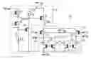
FIG. 1 is a schematic diagram of an electronic circuit 10 comprising a reference generator 12 connected to a comparator 14 in accordance with an embodiment of the present invention. Reference generator 12 comprises two diode connected P-channel insulated gate field effect transistors (IGFETs) 16 and 18, a P-channel IGFET 20, a P-channel IGFET 26, and two current sources 22 and 24. More particularly, the source of IGFET 16 is coupled for receiving a reference voltage VREF and the gate of P-channel IGFET 16 is connected to its drain. The body of P-channel IGFET 16 is connected to its source. The drain of P-channel IGFET 16 is connected to the source of P-channel IGFET 18. The gate of P-channel IGFET 18 is connected to its drain, and the body of P-channel IGFET 18 is connected to its source. The gate of P-channel IGFET 20 is connected to the gate and to the drain of P-channel IGFET 18, the source of P-channel IGFET 20 is coupled for receiving a source of operating potential VDD through current source 22, and the drain of P-channel IGFET 20 is coupled for receiving a source of operating potential VSS. The body of P-channel IGFET 20 is connected to its source. The gates of P-channel IGFETs 18 and 20 are coupled for receiving the source of operating potential VSS through a current source 24. P-channel IGFET 26 has a gate connected to the source of P-channel IGFET 20 and to current source 22, a source connected for receiving source of operating potential VDD, and a body connected to its source. It should be understood that for an IGFET, the drain and source may be referred to as current carrying electrodes and the gate may be referred to as a control electrode. The body may also be referred to as a body region.
Comparator 14 comprises a pair of differentially configured P-channel IGFETs 28 and 30 and a pair of current mirrors 32 and 34. The sources of P-channel IGFETs 28 and 30 are commonly connected to each other and to the drain of P-channel IGFET 26. The gates of P-channel IGFETs 28 and 30 are coupled for receiving input signals VI1 and VI2, respectively. The bodies of IGFETs 28 and 30 are coupled for receiving source of operating potential VDD.
Current mirror 32 comprises a pair of N-channel IGFETs 36 and 38 having commonly connected gates and commonly connected sources, which commonly connected sources are coupled for receiving source of operating potential VSS. The gates of N-channel IGFETs 36 and 38 are connected to each other and to the drains of P-channel IGFET 28 and N-channel IGFET 36. The commonly connected gate and drain of N-channel IGFET 36 may be referred to as an input terminal of current mirror 32 and the drain of IGFET 38 may be referred to as a mirror or output terminal of current mirror 32. The drain of P-channel IGFET 28 is connected to the drain of N-channel IGFET 36. The commonly connected drains of IGFETs 28 and 36 serve as an output 44 of comparator 14 for outputting an output signal VO1. The drain of N-channel transistor 38 is connected to the drains of P-channel IGFET 30 and N-channel IGFET 42.
Current mirror 34 comprises a pair of N-channel IGFETs 40 and 42 having commonly connected gates and commonly connected sources, which sources are coupled for receiving source of operating potential VSS. The commonly connected gates of N-channel IGFETs 40 and 42 are connected to each other and to the drains of P-channel IGFET 30 and N-channel IGFET 42. The commonly connected gate and drain of N-channel IGFET 42 may be referred to as an input terminal of current mirror 34 and the drain of IGFET 40 may be referred to as a mirror or output terminal of current mirror 34. The drain of P-channel IGFET 30 is connected to the drain of N-channel IGFET 42 and serves as an output 46 of comparator 14 for outputting an output signal VO2. The drain of N-channel transistor 40 is also connected to the drains of P-channel IGFET 28 and N-channel IGFET 36.
In operation, a reference voltage VREF is applied to the drain of P-channel IGFET 16 which turns on P-channel IGFETs 16 and 18. Turning on P-channel IGFETs 16 and 18 raises the voltage at the gate of P-channel IFGET 20, thereby turning it on. Turning on P-channel IGFETs 16, 18, and 20 enables current sources 22 and 24 to conduct currents Ia and Ib, respectively. In response to P-channel IGFETs 16, 18, and 20 and current sources 22 and 24 being on, a gate voltage VGATE26 appears at the gate of P-channel IGFET 26 which is given by Equation 1 (Eqt. 1) as:
VGATE26=VREF−VT Eqt. 1
where:
-
- VREF is the reference voltage applied at the source of P-channel IGFET 16; and
- VT is the threshold voltage of P-channel IFGETs 16, 18, or 20.
Gate voltage VGATE26 turns on P-channel IGFET 26 such that it operates in saturation mode having a gate-to-source voltage Vgs26. Gate-to-source voltage Vgs26 is given by Equation 2 (Eqt. 2) as:
Vgs26=VREF−VT−VDD Eqt. 2
where:
-
- VREF is the reference voltage applied at the source of P-channel IGFET 16;
- VT is the threshold voltage of P-channel IFGETs 16, 18, and 20; and
- VDD is a source of operating potential.
Equation 2 is derived using Kirchoffs Voltage Law and the equations for the gate-to-source voltages of P-channel IGFETs 16, 18, and 20. The gate-to-source voltages of P-channel IGFETs 16, 18, and 20 are given by Equations 3, 4, and 5, respectively.
Vgs16=−(((Ib*2*L16)/(k′*W16))(1/2)+VT) Eqt. 3
Vgs18=−(((Ib*2*L18)/(k′*W18))(1/2)+VT) Eqt. 4
Vgs20=−(((Ia*2*L20)/(k′*W20))(1/2)+VT) Eqt. 5
where:
-
- Vgs16 is the gate-to-source voltage of IGFET 16 operating in saturation mode;
- Vgs18 is the gate-to-source voltage of IGFET 18 operating in saturation mode;
- Vgs20 is the gate-to-source voltage of IGFET 20 operating in saturation mode;
- Ia is the current sourced by current source 22;
- Ib is the current sourced by current source 24;
- L16, L18, and L20 are the lengths of P-channel IGFETs 16, 18, and 20, respectively;
- W16, W18, and W20 are the widths of P-channel IGFETs 16, 18, and 20, respectively;
- VT is the threshold voltage of P-channel IGFETs 16, 18, and 20, respectively; and
- k′ is the process transconductance parameter.
From Kirchoffs Voltage Law:
Vgs26=VREfVgs20+Vgs18+Vgs16−VDD Eqt. 6
Substituting Equations 3-5 into Equation 6 and rearranging the terms yields Equation 7:
Vgs26=VREF−VT−VDD−VX Eqt. 7
where:
VX=((Ia*2*L20)/(k′*W20))(1/2)+((Ib*2*L18)/(k′*W18))(1/2)+((Ib*2*L16)/(k′*W16))(1/2)
Equation 2 is derived by setting VX equal to zero. In accordance with one embodiment, VX is set to zero by setting:
Ia=4*Ib;
W16=W18=W20; and
L16=L18=L20.
In accordance with another embodiment, VX is set to zero by setting:
L20=4*L16=4*L18;
W16=W18=W20; and
Ia=Ib.
P-channel IGFET 26 having a gate-to-source voltage Vgs26 generates a drain current ID26 given by Equation 8:
ID26=k′*(W26/L26)*(0.5)*(Vgs26−VT)2(1+λ*Vds26) Eqt. 8
where:
-
- k′ is the process transconductance parameter;
- W26 is the width of P-channel IGFET 26;
- L26 is the length of P-channel IGFET 26;
- Vgs26 is the gate-to-source voltage of P-channel IGFET 26;
- Vds26 is the drain-to-source voltage of P-channel IGFET 26; and
- λ is the channel-length modulation parameter.
The channel length modulation parameter λ is typically very small and therefore the parameter (1+λ*Vds26) can be ignored. Under this condition, the drain current ID26 becomes:
ID26=k′*(W26/L26)*(0.5)*(Vgs26−VT)2 Eqt. 9
Substituting Eqt. 2 into Eqt. 9 gives a drain current that is proportional to the process transconductance parameter k′ as given be Equation 10:
ID26=k′*(W26/L26)*(0.5)*(VREF−VDD)2 Eqt. 10
Thus, P-channel IGFET 26 serves as a current source for comparator 14 that generates a drain current ID26 that is proportional to the process transconductance parameter k′.
Comparator 14 includes a differential input stage comprising P-channel IGFETs 28 and 30 and uses two feedback paths to provide hysteresis. Preferably, the feedback paths are positive feedback paths. The hysteresis, Vhyst, is determined using Equation 10 and the assumption that comparator 14 has already switched:
Vhyst=Vgs30−Vgs28 Eqt. 11
where:
-
- Vgs28 is the gate-to-source voltage of P-channel IGFET 28; and
- Vgs30 is the gate-to-source voltage of P-channel IGFET 30.
- Gate-to-source voltages VGS28 and VGS30 for transistors 28 and 30, respectively, are given by Equations 12 and 13, respectively:
Vgs28=−(((ID28*2*L28)/(k′*W28))(1/2)+VT) Eqt. 12
Vgs30=−(((ID30*2*L30)/(k′*W30))(1/2)+VT) Eqt. 13
where: - ID28 and ID30 are the drain currents flowing through P-channel IGFETs 28 and 30, respectively;
- L28 and L30 are the channel lengths of P-channel IGFETs 28 and 30, respectively;
- W28 and W30 are the channel widths of P-channel IGFETs 28 and 30, respectively;
- VT is the threshold voltage for P-channel IGFETs 28 and 30, respectively; and
- k′ is the process transconductance parameter.
Currents ID28 and ID30 can be expressed in terms of drain current ID26 using Equations 14 and 15, respectively:
ID28=ID26/(1+N) Eqt. 14
ID30=N*ID26/(1+N) Eqt. 15
where:
N=(W38/L38)/(W36/L36)=(W40/L40)/(W42/L42) Eqt. 16
Substituting Equation 16 into Equations 14 and 15 yields substituted Equations 14 and 15 which are then substituted into Equations 11 and 12, respectively, to yield Equation 17, i.e., an equation for hysteresis voltage Vhyst:
V
hyst
=
V
gs
30
-
V
gs
28
=
(
(
I
D
26
*
2
*
L
30
)
/
(
k
′
*
W
30
*
(
1
+
N
)
)
)
(
1
/
2
-
(
(
I
D
26
*
2
*
L
28
*
N
)
/
(
k
′
*
W
28
*
(
1
+
N
)
)
)
(
1
/
2
Eqt
.
17
Setting A=(W26/L26)/(W28/L28), setting (W28/L28)=(W30/L30), substituting these values into Equation 17, and rearranging the equation yields the hysteresis voltage Vhyst as given by Equation 18:
Vhyst=((N/(1+N))1/2−(1/(1+N))1/2)*(VREF−VDD)*(A)1/2 Eqt. 18
Thus, a comparator has been provided having hysteresis that is independent of the process transconductance parameters of the transistors making up the comparator and, therefore, independent of temperature. In accordance with this embodiment, the hysteresis voltage is dependent upon the ratios of the lengths and widths of the IGFETs and reference voltage VREF. An advantage of the present invention is that transistor parameters such as lengths and widths can be well controlled and therefore parameters or characteristics such as hysteresis can also be well controlled.
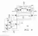
FIG. 2 is a schematic diagram of an electronic circuit 100 comprising a reference generator 102 connected to comparator 14 in accordance with another embodiment of the present invention. Reference generator 102 comprises two diode connected P-channel IGFETs 104 and 106, a P-channel (IGFET) 108, P-channel IGFET 26, and a current mirror 110. More particularly, the source of P-channel IGFET 104 is coupled for receiving source of operating potential VDD, the gate of P-channel IGFET 104 is connected to its drain, and the body of P-channel IGFET 104 is connected to its source. The drain of P-channel IGFET 104 is connected to the source of P-channel IGFET 106 and the gate of P-channel IGFET 106 is connected to its drain. The body of P-channel IGFET 106 is connected to its source and the drain of P-channel IGFET 106 is connected to current mirror 110. The source of P-channel IGFET 108 is connected to its body and for receiving source of operating potential VDD. The gate of P-channel IGFET 108 is coupled for receiving a reference voltage VREF and the drain of P-channel IGFET 108 is connected to current mirror 110. The drain of P-channel IGFET 106 is connected to the gate of P-channel IGFET 26.
Current mirror 110 comprises a pair of N-channel IGFETs 112 and 114. The drain of N-channel IGFET 112 is connected to the drain of P-channel IGFET 108, the source of N-channel IGFET 112 is coupled to the source of N-channel IGFET 114 and for receiving source of operating potential VSS. The gates of N-channel IGFETs 112 and 114 are commonly connected to each other and to the drains of P-channel IGFET 108 and N-channel IGFET 112. The drain of N-channel IGFET 114 is connected to the drain of P-channel IGFET 106 and to the gate of P-channel IGFET 26. The commonly connected gate and drain of N-channel IGFET 112 may be referred to as an input terminal of current mirror 110 and the drain of N-channel IGFET 114 may be referred to as a mirror or output terminal of current mirror 110.
In operation, a reference voltage VREF is applied to the drain of P-channel IGFET 108, causing a current ID108 to flow. Current mirror 110 mirrors current ID108 such that P-channel IGFETs 104 and 106 operate in saturation mode and a current IM110 flows through IGFETs 104, 106, and 114. In response to current IM110, a voltage VGATE26 appears at the gate of P-channel IGFET 26 such that it operates in saturation mode. Gate voltage VGATE26 is given by Equation 19 (Eqt. 19) as:
VGATE26=VREF−VT Eqt. 19
where:
-
- VREF is the reference voltage applied at the gate of P-channel IGFET 108; and
- VT is the threshold voltage of P-channel IFGETs 104, 106, and 108.
Thus, P-channel IGFET 26 has a gate-to-source voltage Vgs26 given by Equation 20 (Eqt. 20) as:
Vgs26=VREF−VT−VDD Eqt. 20
where:
-
- VREF is the reference voltage applied at the gate of P-channel IGFET 108;
- VT is the threshold voltage of P-channel IGFETs 104, 106, 108, and 26; and
- VDD is a source of operating potential.
Equation 20 is derived using Kirchoff's Voltage Law and the equations for the gate-to-source voltages of P-channel IGFETs 104, 106, 108, and 26. The gate-to-source voltages of P-channel IGFETs 104, 106, 108, and 26 are given by Equations 21, 22, 23, and 24, respectively, as:
Vgs104=−(((IM110*2*L104)/(k′*W104))(1/2)+VT) Eqt. 21
Vgs106=−(((IM110*2*L106)/(k′*W106))(1/2)+VT) Eqt. 22
Vgs108=−(((ID108*2*L108)/(k′*W108))(1/2)+VT) Eqt. 23
Vgs26=−(((ID26*2*L26)/(k′*W26))(1/2)+VT) Eqt. 24
where:
-
- Vgs104 is the gate-to-source voltage of IGFET 104 operating in saturation mode;
- Vgs106 is the gate-to-source voltage of IGFET 106 operating in saturation mode;
- Vgs108 is the gate-to-source voltage of IGFET 108 operating in saturation mode;
- Vgs26 is the gate-to-source voltage of IGFET 26 operating in saturation mode;
- ID108 is the drain current of IGFET 108 operating in saturation mode;
- IM110 is the drain current of IGFETs 104, 106, and 114, i.e., it is a mirrored current;
- L104, L106, L108, and L26 are the lengths of P-channel IGFETs 104, 106, 108, and 26, respectively;
- W104, W106, W108, and W26 are the widths of P-channel IGFETs 104, 106, 108, and 26, respectively;
- VT is the threshold voltage of P-channel IGFETs 104, 106, 108, and 26; and
- k′ is the process transconductance parameter.
From Kirchoff's Voltage Law:
Vgs26=VREF−Vgs108+Vgs104+Vgs106−VDD Eqt. 25
Substituting Equations 21-24 into Equation 25 and rearranging the terms yields Equation 26:
Vgs26=VREF−VT−VDD−Vz Eqt. 26
where:
VZ=((ID108*2*L108)/(k′*W108))(1/2)−((IM110*2*L104)/(k′*W104))(1/2)−((IM110*2*L106)/(k′*W106))(1/2)
Equation 20 is derived by setting voltage VZ equal to zero. In accordance with one embodiment, VZ is set to zero by setting:
IM110=4*ID108;
W104=W106=W108; and
L104=L106=L108.
In accordance with another embodiment, VZ is set to zero by setting:
L104=L106=4*L108;
W104=W106=W108; and
ID108=IM110.
Like the embodiment shown in FIG. 1, P-channel IGFET 26 generates a drain current ID26 given by Equation 8 and comparator 14 has a hysteresis voltage, Vhyst, given by Equation 18.
FIG. 3 is a schematic diagram of an electronic circuit 200 comprising a reference generator 202 connected to a comparator 204 in accordance with another embodiment of the present invention. Reference generator 202 comprises two diode connected N-channel IGFETs 206 and 208, an N-channel IGFET 210, an N-channel IGFET 216, and two current sources 212 and 214. More particularly, the source of N-channel IGFET 206 is coupled for receiving reference voltage VREF and the gate of N-channel IGFET 206 is connected to its drain. The body of N-channel IGFET 206 is connected to its source. The drain of N-channel IGFET 206 is connected to the source of N-channel IGFET 208. The body of N-channel IGFET 208 is connected to its source and the gate of N-channel IGFET 208 is connected to its drain. The gate of N-channel IGFET 210 is connected to the gate and drain of N-channel IGFET 208, the source on N-channel IGFET 210 is coupled for receiving a source of operating potential VSS through current source 212, and the drain of N-channel IGFET 210 is coupled for receiving a source of operating potential VDD. The body of N-channel IGFET 210 is connected to its source. In addition, the gate of N-channel IGFET 210 and the drain of N-channel IGFET 208 are coupled for receiving the source of operating potential VDD through a current source 214.
N-channel IGFET 216 has a gate connected to the source of N-channel IGFET 210 and to current source 212, a source connected for receiving source of operating potential VDD, and a body connected to its source.
Comparator 204 comprises a pair of differentially configured N-channel IGFETs 218 and 220 and a pair of current mirrors 222 and 224. The sources of P-channel IGFETs 218 and 220 are commonly connected to each other and to the drain of IGFET 216. The gates of IGFETs 218 and 220 are coupled for receiving input signals VI1 and VI2, respectively. The bodies of IGFETs 218 and 220 are coupled for receiving source of operating potential VSS. Current mirror 222 comprises a pair of P-channel IGFETs 226 and 228 having commonly connected gates and commonly connected sources, which commonly connected sources are coupled for receiving source of operating potential VDD. The commonly connected gates of P-channel IGFETs 226 and 228 are connected to the drains of N-channel IGFET 218 and P-channel IGFET 226. Thus, the drain of N-channel IGFET 218 is connected to the drain of P-channel IGFET 226. The commonly connected drains of IGFETs 218 and 226 serve as an output 230 of comparator 214 for outputting an output signal VO1. The drain of P-channel transistor 228 is connected to the drains of N-channel IGFET 220 and P-channel IGFET 234.
Current mirror 224 comprises a pair of P-channel IGFETs 232 and 234 having commonly connected gates and commonly connected sources, which sources are coupled for receiving source of operating potential VDD. The commonly connected gates of N-channel IGFETs 232 and 234 are connected to the drains of N-channel IGFET 220 and P-channel IGFET 234. The drain of N-channel IGFET 220 is connected to the drain of P-channel IGFET 234 and serves as an output 240 of comparator 14 for outputting an output signal VO2. The drains of N-channel IGFET 220 and P-channel IGFET 234 are also connected to the drain of P-channel transistor 228.
The operation of electronic circuit 200 is similar to that of electronic circuits 10 and 100 except the equations are modified to account for the P-channel IGFETs of electronic circuit 10 that have been switched to N-channel IGFETs and for the N-channel IGFETs that have been switched to P-channel IGFETs.
By now it should be appreciated that a circuit and method for generating a voltage dependent on the threshold voltage of an IGFET and for generating a drain current proportional to a process transconductance parameter have been provided. Because of the dependence on threshold voltage, the circuit can be used in combination with other circuits to generate electrical signals that are independent of temperature. Although, the generation and use of a current proportional to the process transconductance parameter in conjunction with a comparator has been shown, this is not a limitation of the present invention. Temperature effects associated with other circuits can also be negated or nullified.
Although certain preferred embodiments and methods have been disclosed herein, it will be apparent from the foregoing disclosure to those skilled in the art that variations and modifications of such embodiments and methods may be made without departing from the spirit and scope of the invention. It is intended that the invention shall be limited only to the extent required by the appended claims and the rules and principles of applicable law.
Claims
What is claimed is:1. A method for nullifying temperature dependence associated with a transconductance, comprising:
generating a first current that is proportional to a first transconductance; and
using the first current to generate an output that is substantially independent of the first transconductance.
2. The method of claim 1, wherein generating the first current includes generating the first current to be substantially independent of the threshold voltage of a first insulated gate field effect transistor.
3. The method of claim 2, wherein generating the first current includes applying a voltage to a gate of the first insulated gate field effect transistor, the voltage having a threshold voltage component from a second insulated gate field effect transistor.
4. The method of claim 3, wherein generating the first current includes using means for generating the voltage, wherein the voltage is a difference between a reference voltage and the threshold voltage component from the second insulated gate field effect transistor.
5. The method of claim 1, wherein using the first current to generate an output that is substantially independent of the first transconductance includes:
providing a second insulated gate field effect transistor having a second transconductance; and
using the second insulated gate field effect transistor and a portion of the first current to nullify the temperature effect of the first transconductance parameter.
6. The method of claim 5, wherein using the second insulated gate field effect transistor and the portion of the first current to nullify the temperature effect of the first transconductance parameter includes ratioing the first and second transconductance parameters to generate a first constant.
7. The method of claim 5, further including:
providing a third insulated gate field effect transistor having a third device transconductance parameter; and
using the third insulated gate field effect transistor and another portion of the first current to nullify the temperature effect of the first transconductance parameter.
8. A method for negating a temperature component of an electrical signal, comprising:
generating a current that is proportional to a first process transconductance parameter; and
using a portion of the current to generate a first voltage, wherein the first voltage includes a component having a second process transconductance parameter, and wherein a ratio of the first process transconductance parameter to the second process transconductance parameter is substantially constant and substantially independent of temperature.
9. The method of claim 8, wherein generating the current includes applying a second voltage to a gate of first insulated gate field effect transistor, the second voltage having a component substantially equal to a threshold voltage of the first insulated gate field effect transistor.
10. The method of claim 9, further including generating the second voltage to include a term that is one of a sum of a reference voltage and threshold voltage of a second insulated gate field effect transistor or a difference between the reference voltage and the threshold voltage of the second insulated gate field effect transistor and using another portion of the current to generate a third voltage, wherein the third voltage has as third process transconductance parameter, and wherein a ratio of the first process transconductance parameter to the third transconductance component is substantially constant and substantially independent of temperature.
11. A method for nullifying a temperature dependence of a characteristic associated with a circuit, comprising:
generating a first current having a first transconductance value;
supplying the first current to the circuit, the circuit having a characteristic and a second transconductance, wherein the characteristic of the circuit is substantially independent of temperature.
12. The method of claim 11, wherein the characteristic is a measurable characteristic.
13. The method of claim 12, wherein the measurable characteristic is hysteresis.
14. The method of claim 11, wherein the circuit comprises a comparator.
15. The method of claim 11, further including taking a ratio of the first transconductance to the second transconductance to nullify the temperature dependence of the characteristic.
16. A circuit, comprising:
a conductor for transmitting a current proportional to a first process transconductance parameter; and
a circuit coupled to the conductor, wherein the circuit cooperates with the conductor to negate a temperature component of an output signal.
17. The circuit of claim 16, further including:
a first semiconductor device having first and second current carrying electrodes;
a second semiconductor device having first and second current carrying electrodes, the first current carrying electrode of the second semiconductor device coupled to the second current carrying electrode of the first semiconductor device;
a third semiconductor device having a control electrode and first and second current carrying electrodes, the control electrode coupled to the second current carrying electrode of the second semiconductor device;
a first current source coupled between the second current carrying electrode of the second semiconductor device and a first source of operating potential; and
a second current source coupled between the first current carrying electrode of the third semiconductor device and a second source of operating potential.
18. The circuit of claim 17, wherein the first, second, and third semiconductor devices are P-channel insulated gate field effect transistors.
19. The circuit of claim 17, further including a fourth semiconductor device having a control electrode and first and second current carrying electrodes, the control electrode coupled to the first current carrying electrode of the third semiconductor device, the first current carrying electrode coupled for receiving a source of operating potential, and the second current carrying electrode serving as the conductor for transmitting a current proportional to a first process transconductance parameter.
20. The circuit of claim 19, wherein the circuit comprises a comparator.
21. The circuit of claim 20, wherein the comparator comprises:
a fifth semiconductor device having a control electrode, first and second current carrying electrodes, and a body region, the first current carrying electrode of the fifth semiconductor device coupled to the conductor for transmitting a current proportional to a first process transconductance parameter;
a sixth semiconductor device having a control electrode, first and second current carrying electrodes, and a body region, the first current carrying electrode of the sixth semiconductor device coupled to the conductor for transmitting a current proportional to a first process transconductance parameter;
a first current mirror having an input terminal and a mirror terminal, the input terminal coupled to the second current carrying electrode of the fifth semiconductor device and the mirror terminal coupled to the second current carrying electrode of the sixth semiconductor device; and
a second current mirror having an input terminal and a mirror terminal, the input terminal coupled to the second current carrying electrode of the sixth semiconductor device and the mirror terminal coupled to the second current carrying electrode of the fifth semiconductor device.
Images & Drawings included:

Sources:
- United States Patent and Trademark Office - verify current appl. status at the USPTO↗
Recent applications in this class:
- » 20250233564 2025-07-17
SYSTEM AND METHOD FOR CROSS-COUPLED RC NETWORKS FOR USE IN DIFFERENTIAL AMPLIFIERS AND OTHER CIRCUITS - » 20250112602 2025-04-03
MULTI-GATE DIFFERENTIAL POWER AMPLIFIER - » 20240313721 2024-09-19
POWER EFFICIENT COMPLEMENTARY AMPLIFIER AND METHOD THEREOF - » 20240258979 2024-08-01
INTRINSIC MOS CASCODE DIFFERENTIAL INPUT PAIR - » 20220286100 2022-09-08
Comparator, photoelectric conversion device, and apparatus - » 20220278661 2022-09-01
Operational amplifier - » 20220200553 2022-06-23
SEMICONDUCTOR INTEGRATED CIRCUIT - » 20210359655 2021-11-18
Linear amplifier - » 20210313941 2021-10-07
Apparatus and method for an analog to digital converter - » 20210203291 2021-07-01
Current integrator for OLED panel
Recent applications for this Assignee:
- » 20240348142 2024-10-17
LOW POWER GREEN MODE FOR MULTI-PHASE POWER CONVERTERS - » 20240290757 2024-08-29
SANDWICH PACKAGE FOR MICROELECTRONICS - » 20240290736 2024-08-29
MOLDED THIN SEMICONDUCTOR DIE PACKAGES AND RELATED METHODS - » 20240282668 2024-08-22
PROTECTION DAM FOR A POWER MODULE WITH SPACERS - » 20240275272 2024-08-15
Methods and systems of power-factor-correction converters - » 20240274506 2024-08-15
JET IMPINGEMENT HEATSINK FOR HIGH POWER SEMICONDUCTOR DEVICES - » 20240266264 2024-08-08
SEMICONDUCTOR PACKAGES WITH WETTABLE FLANKS AND RELATED METHODS - » 20240266252 2024-08-08
SINGLE SWITCH DIRECT COOLING ASSEMBLIES AND RELATED METHODS - » 20240259701 2024-08-01
Methods for mitigating lag in image sensor devices - » 20240258181 2024-08-01
Substrates and related methods