Photosensing soluble organic semiconductor material
US20070262298A1
2007-11-15
11/552,990
2006-10-26
✅ Patent granted
US 7,820,653 B2
2010-10-26
-
-
James O Wilson | Brian McDowell
2029-03-23
Abstract:
A photosensing soluble organic semiconductor material is disclosed, which includes a Diels-Alder adduct which is a polycyclic aromatic compound with a dienophile. The polycyclic aromatic compound is selected from the group consisting of oligothiophene, perylene, benzo[ghi]perylene, coronene and polyacene. And the dienophile is represented by the formula of O═S═N—R1, wherein R1 is SO2R2, SO3R2, SO2−, or SO3−; and wherein R2 is selected from the group consisting of alkyl, alkoxy, acyl, aryl, aralkyl, chloroalkyl, fluoroalkyl, and substituted aryl with 1-12 carbon atoms.
Inventors:
- Jia-Chong Ho 18 🇹🇼 Hsinchu County, Taiwan
- Tarng-Shiang Hu 23 🇹🇼 Hsinchu City, Taiwan
- Hsiang-Yuan Cheng 8 🇹🇼 Taipei City, Taiwan
- Tarng-Shiang Hu 24 🇹🇼 Hsinchu, Taiwan
- Tzu-Wei Lee 1 🇹🇼 Chiayi City, Taiwan
- Ming-Chou Chen 1 🇹🇼 Hsinchu City, Taiwan
- Jen-Shyang Ni 1 🇹🇼 Changhua County, Taiwan
- Hsiang-Yuan Cheng 5 🇹🇼 Taipei, Taiwan
- Tzu-Wei Lee 1 🇹🇼 Chiayi, Taiwan
- Ming-Chou Chen 1 🇹🇼 Hsinchu, Taiwan
Assignee:
- INDUSTRIAL TECHNOLOGY RESEARCH INSTITUTE 7,890 🇹🇼 HSINCHU, Taiwan
Interested in similar patents?
Get notified when new applications in this technology area are published.
Classification:
C07D513/08 » CPC main
Heterocyclic compounds containing in the condensed system at least one hetero ring having nitrogen and sulfur atoms as the only ring hetero atoms, not provided for in groups , or - in which the condensed system contains two hetero rings Bridged systems
H01L51/0015 » CPC further
Solid state devices using organic materials as the active part, or using a combination of organic materials with other materials as the active part; Processes or apparatus specially adapted for the manufacture or treatment of such devices, or of parts thereof; Processes specially adapted for the manufacture or treatment of devices or of parts thereof for changing the shape of the device layer, e.g. patterning by selective transformation of an existing layer
H01L51/0018 » CPC further
Solid state devices using organic materials as the active part, or using a combination of organic materials with other materials as the active part; Processes or apparatus specially adapted for the manufacture or treatment of such devices, or of parts thereof; Processes specially adapted for the manufacture or treatment of devices or of parts thereof for changing the shape of the device layer, e.g. patterning etching of an existing layer using photolithographic techniques
H01L51/0053 » CPC further
Solid state devices using organic materials as the active part, or using a combination of organic materials with other materials as the active part; Processes or apparatus specially adapted for the manufacture or treatment of such devices, or of parts thereof; Selection of organic semiconducting materials, e.g. organic light sensitive or organic light emitting materials; Macromolecular systems with low molecular weight, e.g. cyanine dyes, coumarine dyes, tetrathiafulvalene; Polycyclic condensed aromatic hydrocarbons, e.g. anthracene Aromatic anhydride or imide compounds, e.g. perylene tetra-carboxylic dianhydride, perylene tetracarboxylic diimide
H01L51/0055 » CPC further
Solid state devices using organic materials as the active part, or using a combination of organic materials with other materials as the active part; Processes or apparatus specially adapted for the manufacture or treatment of such devices, or of parts thereof; Selection of organic semiconducting materials, e.g. organic light sensitive or organic light emitting materials; Macromolecular systems with low molecular weight, e.g. cyanine dyes, coumarine dyes, tetrathiafulvalene; Polycyclic condensed aromatic hydrocarbons, e.g. anthracene containing five rings, e.g. pentacene
H01L51/0056 » CPC further
Solid state devices using organic materials as the active part, or using a combination of organic materials with other materials as the active part; Processes or apparatus specially adapted for the manufacture or treatment of such devices, or of parts thereof; Selection of organic semiconducting materials, e.g. organic light sensitive or organic light emitting materials; Macromolecular systems with low molecular weight, e.g. cyanine dyes, coumarine dyes, tetrathiafulvalene; Polycyclic condensed aromatic hydrocarbons, e.g. anthracene containing six or more rings
H01L51/0508 » CPC further
Solid state devices using organic materials as the active part, or using a combination of organic materials with other materials as the active part; Processes or apparatus specially adapted for the manufacture or treatment of such devices, or of parts thereof specially adapted for rectifying, amplifying, oscillating or switching, or capacitors or resistors with at least one potential- jump barrier or surface barrier multistep processes for their manufacture the devices being controllable only by the electric current supplied or the electric potential applied, to an electrode which does not carry the current to be rectified, amplified or swiched, e.g. three-terminal devices Field-effect devices, e.g. TFTs
H01L51/00 IPC
Solid state devices using organic materials as the active part, or using a combination of organic materials with other materials as the active part; Processes or apparatus specially adapted for the manufacture or treatment of such devices, or of parts thereof
C07D513/00 IPC
Heterocyclic compounds containing in the condensed system at least one hetero ring having nitrogen and sulfur atoms as the only ring hetero atoms, not provided for in groups , or -
A61K31/5415 IPC
Medicinal preparations containing organic active ingredients; Heterocyclic compounds having nitrogen as a ring hetero atom, e.g. guanethidine or rifamycins having six-membered rings with at least one nitrogen and one sulfur as the ring hetero atoms, e.g. sulthiame ortho- or peri-condensed with carbocyclic ring systems, e.g. phenothiazine, chlorpromazine, piroxicam
Description
CROSS-REFERENCE TO RELATED APPLICATION
This application claims the priority benefit of Taiwan application serial no. 95116329, filed on May 9, 2006. All disclosure of the Taiwan application is incorporated herein by reference.
BACKGROUND OF THE INVENTION
1. Field of Invention
The present invention relates to a semiconductor material applied in an organic thin film transistor (OTFT). More particularly, the present invention relates to a photosensing soluble organic semiconductor material.
2. Description of Related Art
The greatest difference between an organic thin film transistor and a Metal Oxide Semiconductor (MOS) transistor is that an organic semiconductor material is utilized in the organic thin film transistor to replace an inorganic semiconductor material used in the MOS transistor. Generally, the organic thin film transistor is a transistor made from an organic conjugated polymer or oligomer material. Compared with the traditional inorganic transistor, the organic thin film transistor can be prepared at low temperature, thus a lighter, thinner, and cheaper plastics can be employed to substitute the glass as a substrate.
Moreover, the process of an organic thin film transistor is simple, including directly patterning an organic thin film with a printing technique, which can reduce the number of the masks and decrease the usage cost of the vacuum vapor deposition apparatus, and is highly compatible with subsequent roll to roll continuous process because of being suitable for plastics substrates, thus greatly reducing the manufacturing cost.
SUMMARY OF THE INVENTION
Accordingly, the present invention is directed to provide a photosensing soluble organic semiconductor material, so that the organic thin film transistor (OTFT) may have more opportunities to be applied in electronic products with low cost and large areas.
Another object of the present invention is to provide a photosensing soluble organic semiconductor material, which can reduce the number of the masks and decrease the usage cost of the vacuum vapor deposition apparatus, i.e., which can be applied in the manufacture of electronic products with low cost and large areas.
The present invention proposes a photosensing soluble organic semiconductor material including an adduct obtained from the Diels-Alder reaction, which adduct is a polycyclic aromatic compound with a dienophile. The polycyclic aromatic compound is selected from the group consisting of oligothiophene, perylene, benzo[ghi]perylene, coronene, and polyacene. And the dienophile is represented by the formula of O═S═N—R1, wherein R1 is SO2R2 or SO3R2, and wherein R2 is selected from the group consisting of alkyl, alkoxy, acyl, aryl, aralkyl, chloroalkyl, fluoroalkyl, and substituted aryl of 1-12 carbon atoms. The substituted aryl has a substituent selected from the group consisting of —F, —Cl, —Br, —NO2, —CO2R, —PO3H, —SO3H, —SO2R, —SO3R, trialkylsilyl, and acyl.
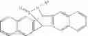
According to the photosensing soluble organic semiconductor material described in one embodiment of the present invention, the structural formula of the adduct is as follows:
According to the photosensing soluble organic semiconductor material described in one embodiment of the present invention, the structural formula of the adduct is as follows:
According to the photosensing soluble organic semiconductor material described in one embodiment of the present invention, the structural formula of the adduct is as follows:
According to the photosensing soluble organic semiconductor material described in one embodiment of the present invention, the polycyclic aromatic compound includes a polyacene, and the structural formula of the polyacene is as follows:
wherein n is at least 2.
According to the photosensing soluble organic semiconductor material described in one embodiment of the present invention, the polyacene may be penracene.
The present invention further proposes a photosensing soluble organic semiconductor material including an adduct obtained from the Diels-Alder reaction, which adduct is a polycyclic aromatic compound with a dienophile, wherein the polycyclic aromatic compound is selected from the group consisting of oligothiophene, perylene, benzo[ghi]perylene, coronene, and polyacene. And the dienophile is represented by the formula of O═S═N—R1, wherein R1 is SO2− or SO3−.
According to the photosensing soluble organic semiconductor material described in another embodiment of the present invention, the structural formula of the adduct is as follows:
According to the photosensing soluble organic semiconductor material described in another embodiment of the present invention, the structural formula of the adduct is as follows:
According to the photosensing soluble organic semiconductor material described in another embodiment of the present invention, the structural formula of the adduct is as follows:
According to the photosensing soluble organic semiconductor material described in another embodiment of the present invention, the polycyclic aromatic compound includes a polyacene, and the structural formula of the polyacene is as follows:
wherein n is at least 2.
According to the photosensing soluble organic semiconductor material described in another embodiment of the present invention, the polyacene is, for example, penracene.
The present invention enables the organic thin film transistor (OTFT) to be applied in electronic products with low cost and large areas because a micromolecular organic semiconductor material is combined with different functional groups to form a photosensing soluble organic semiconductor material. Moreover, the photosensing soluble organic semiconductor material of the present invention may be formed to a patterned thin film directly by a printing technique, so the number of the masks can be reduced and the usage cost of the vacuum vapor deposition apparatus can be decreased. Additionally, the present invention is highly compatible with subsequent continuous process and is greatly favorable for decreasing the manufacturing cost because it is suitable for plastic substrates, therefore, it can be used in the manufacture of electronic products with low cost and large areas.
In order to make the aforementioned and other objects, features and advantages of the present invention comprehensible, preferred embodiments are exemplified in detail below.
DESCRIPTION OF EMBODIMENTS
The present invention relates to a photosensing soluble organic semiconductor material, mainly by combining a micromolecular organic semiconductor material with different functional groups to form the photosensing soluble organic semiconductor material.
First Embodiment
The photosensing soluble organic semiconductor material in this embodiment includes an adduct obtained from the Diels-Alder reaction, which is also known as the diene addition reaction. And the adduct is a polycyclic aromatic compound with a dienophile.
In the embodiment, the polycyclic aromatic compound is selected from the group consisting of oligothiophene, perylene, benzo[ghi]perylene, coronene, and polyacene.
In the embodiment, the dienophile is represented by the formula of O═S═N—R1, wherein R1 is SO2R2 or SO3R2, and wherein R2 is selected from the group consisting of alkyl, alkoxy, acyl, aryl, aralkyl, chloroalkyl, fluoroalkyl, and substituted aryl of 1-12 carbon atoms. The substituted aryl has a substituent selected from the group consisting of —F, —Cl, —Br, —NO2, —CO2R, —PO3H, —SO3H, —SO2R, —SO3R, trialkylsilyl, and acyl.
An example is proposed to illustrate the first embodiment in detail, but the present invention is not limited to the semiconductor material described in this example.
EXAMPLE 1
When the polycyclic aromatic compound of the photosensing soluble organic semiconductor material in the first embodiment is the polyacene of the following structural formula (1):
wherein n is at least 2,
and the polyacene is penracene (i.e., n is 3), the adduct of the first embodiment is of the following structural formula (2):
As R1 is SO2R2 or SO3R2, the adduct in example 1 may be of either the following structural formula (3) or structural formula (4):
The photosensing soluble organic semiconductor material of the structural formula (3) or structural formula (4) is prepared mainly by combining a micromolecularorganic semiconductor material like polycyclic aromatic compound with the dienophile described in the first embodiment in a Diels-Alder reaction.
For example, the dienophile such as N-sulfinyl-R-sulfonamide or N-sulfinyl-R-amidosulfate can be reacted with a penracene in a Diels-Alder reaction, the reaction equation of which is as follows:
The photosensing soluble organic semiconductor material which acts as the precursor of the organic semiconductor material can be coated onto a substrate directly with the methods of inkjet printing, micro contact printing, nanoimprinting, spin-coating-yellow photolithography, etc. Thereafter, the precursor may be reduced to a micromolecular organic semiconductor by the control of the process, for example, the steps of heating, baking or lighting, etc., so as to achieve the preparation of an organic semiconductor with a solution process. The following is the reaction equation of the reduction of the structural formula (3) of example 1 to a penracene through the steps of heating, baking or lighting, etc.:
Second Embodiment
The greatest difference between the photosensing soluble organic semiconductor material in the second embodiment and that in the first embodiment is that R1 in the formula of dienophile: O═S═N—R1, and R1 is SO2− or SO3−. The polycyclic aromatic compound of the photosensing soluble organic semiconductor material is selected from the group consisting of oligothiophene, perylene, benzo [ghi]perylene, coronene, and polyacene.
An example is proposed to illustrate the second embodiment in detail, but the present invention is not limited to the semiconductor material described in this example.
EXAMPLE 2
When the polycyclic aromatic compound of the photosensing soluble organic semiconductor material in the second embodiment is the polyacene of the following structural formula (1):
wherein n is at least 2,
and the polyacene used in this example 2 is penracene, the adduct of the second embodiment is of either the following structural formula (5) or structural formula (6):
Furthermore, the preparation of the photosensing soluble organic semiconductor material of the structural formula (5) or structural formula (6) is also performed by combining a polycyclic aromatic compound with the dienophile described in the second embodiment in a Diels-Alder reaction, the reaction equation of which is as follows:
Furthermore, the photosensing soluble organic semiconductor material can be coated onto a substrate directly with the methods of inkjet printing, micro contact printing, nanoimprinting, spin-coating-yellow photolithography, etc. Thereafter, it may be reduced to a micromolecular organic semiconductor by the control of the process, for example, the steps of heating, baking or lighting, etc., so as to achieve the preparation of an organic semiconductor with a solution process.
In conclusion, the present invention is characterized by combining a micromolecular organic semiconductor material with different functional groups to form a photosensing soluble organic semiconductor material, thus enabling the organic thin film transistor (OTFT) to be applied in electronic products with low cost and large areas. Moreover, the material of the present invention may be formed to a patterned thin film directly by employing a print technique, so the number of the masks can be reduced while the usage cost of the vacuum vapor deposition apparatus can be decreased. Moreover, the present invention is highly compatible with subsequent continuous process and is greatly favorable for decreasing the manufacturing cost because it is suitable for flexible plastic substrates with low cost, therefore, it can be used in the manufacture of the electronic products with low cost and large areas.
Although the present invention has been disclosed in the preferred embodiments as above, it is not intended to limit the present invention. Various variations and modifications can be made by any of those skilled in the art without deviating from the spirit and scope of the present invention. Therefore, the scope of the present invention depends on that defined in the appended claims.
Claims
What is claimed is:1. A photosensing soluble organic semiconductor material, comprising an adduct obtained from the Diels-Alder reaction, wherein the adduct is a polycyclic aromatic compound with a dienophile, wherein:
the polycyclic aromatic compound is selected from the group consisting of oligothiophene, perylene, benzo[ghi]perylene, coronene, and polyacene; and
the dienophile is represented by the formula of O═S═N—R1,
wherein R1 is SO2R2 or SO3R2, and wherein R2 is selected from the group consisting of alkyl, alkoxy, acyl, aryl, aralkyl, chloroalkyl, fluoroalkyl, and a substituted aryl with 1-12 carbon atoms, and the substituted aryl has a substituent selected from the group consisting of —F, —Cl, —Br, —NO2, —CO2R, —PO3H, —SO3H, —SO2R, —SO3R, trialkylsilyl, and acyl.
2. The photosensing soluble organic semiconductor material as claimed in claim 1, wherein the structural formula of the adduct is as follows:
3. The photosensing soluble organic semiconductor material as claimed in claim 2, wherein the structural formula of the adduct is as follows:
4. The photosensing soluble organic semiconductor material as claimed in claim 2, wherein the structural formula of the adduct is as follows:
5. The photosensing soluble organic semiconductor material as claimed in claim 1, wherein the polycyclic aromatic compound includes a polyacene, and the structural formula of the polyacene is as follows:
wherein n is at least 2.
6. The photosensing soluble organic semiconductor material as claimed in claim 5, wherein the polyacene includes a penracene.
7. A photosensing soluble organic semiconductor material, comprising an adduct obtained from the Diels-Alder reaction, which adduct is a polycyclic aromatic compound with a dienophile, wherein:
the polycyclic aromatic compound is selected from the group consisting of oligothiophene, perylene, benzo[ghi]perylene, coronene, and polyacene; and
the dienophile is represented by the formula of O═S═N—R1,
wherein R1 is SO2− or SO3−.
8. The photosensing soluble organic semiconductor material as claimed in claim 7, wherein the structural formula of the adduct is as follows:
9. The photosensing soluble organic semiconductor material as claimed in claim 8, wherein the structural formula of the adduct is as follows:
10. The photosensing soluble organic semiconductor material as claimed in claim 8, wherein the structural formula of the adduct is as follows:
11. The photosensing soluble organic semiconductor material as claimed in claim 7, wherein the polycyclic aromatic compound includes a polyacene, and the structural formula of the polyacene is as follows:
wherein n is at least 2.
12. The photosensing soluble organic semiconductor material as claimed in claim 11, wherein the polyacene includes a penracene.
Images & Drawings included:


Sources:
- United States Patent and Trademark Office - verify current appl. status at the USPTO↗
Recent applications in this class:
- » 20240199646 2024-06-20
REDOX ACTIVE MATERIALS, PROCESSES AND USES THEREOF - » 20230312602 2023-10-05
SALT FORMS AND SOLVATES OF MCI-1 ANTAGONISTS - » 20230099739 2023-03-30
JAK KINASE INHIBITOR AND PREPARATION AND APPLICATION THEREOF - » 20220411441 2022-12-29
Redox active materials, processes and uses thereof - » 20220017538 2022-01-20
THIOESTER PRODRUGS OF MACROCYCLES AS INHIBITORS OF HISTONE DEACETYLASES - » 20200317693 2020-10-08
Thioester prodrugs of macrocycles as inhibitors of histone deacetylases - » 20200231601 2020-07-23
1,4-thiazine dioxide and 1,2,4-thiadiazine dioxide derivatives as beta-secretase inhibitors and methods of use - » 20190382417 2019-12-19
Alpha-amino pateamine A derivatives and methods for treating chronic lymphocytic leukemia - » 20190177339 2019-06-13
Beta-amino pateamine a derivatives and methods for treating chronic lymphocytic leukemia - » 20180305377 2018-10-25
Epidithiodioxopiperazine compound or its derivatives, and the use thereof
Recent applications for this Assignee:
- » 20250289330 2025-09-18
MOBILE VEHICLE CHARGING PROTECTION DEVICE FOR ELECTRICAL SAFETY IN LIVESTOCK HOUSES - » 20250287224 2025-09-11
COMMUNICATION DEVICE AND COMMUNICATION METHOD - » 20250286593 2025-09-11
COMMUNICATION DEVICE AND METHOD OF BEAM MANAGEMENT - » 20250284336 2025-09-11
SYSTEM AND METHOD FOR ADJUSTING IMAGE BASED ON PHYSIOLOGICAL INFORMATION AND POSTURE - » 20250281908 2025-09-11
ELECTROCATALYST COMPOSITION AND PREPARATION METHOD THEREOF - » 20250273403 2025-08-28
CAPACITOR AND ELECTRONIC DEVICE - » 20250271759 2025-08-28
POLYMER, POSITIVE PHOTORESIST COMPOSITION, AND METHOD FOR FORMING PATTERNED PHOTORESIST LAYER - » 20250265803 2025-08-21
MULTI-SENSOR COORDINATION METHOD, PROCESSING DEVICE, AND INFORMATION DISPLAY SYSTEM - » 20250263659 2025-08-21
METHOD AND KIT FOR PREPARING AN IMMUNE CELL DIFFERENTIATED FROM A STEM CELL - » 20250252547 2025-08-07
CORROSION POSITIONING SYSTEM, CORROSION INSPECTION VEHICLE AND CORROSION POSITIONING METHOD USING THE SAME