METHOD FOR MANUFACTURING MULTILAYER FLEXIBLE PRINTED CIRCUIT BOARD
US20080141527A1
2008-06-19
11/861,650
2007-09-26
Abstract:
The present inventions relates to a method for manufacturing a multilayer FPCB. The method includes the steps of providing three copper clad laminates and two binder layers, each of the copper clad laminates includes a dielectric layer and at least one patterned conductive layer formed on the dielectric layer; stacking the copper clad laminates and the binder layers alternately one on another; aligning the copper clad laminates and the binder layers; and compressing the copper clad laminates and the binder layers together thereby obtaining a multilayer flexible printed circuit board.
Assignee:
- FOXCONN ADVANCED TECHNOLOGY INC. 111 🇹🇼 Tayuan, Taiwan
Interested in similar patents?
Get notified when new applications in this technology area are published.
Classification:
H05K3/4611 » CPC main
Apparatus or processes for manufacturing printed circuits; Manufacturing multilayer circuits by laminating two or more circuit boards
H05K3/4611 » CPC main
Apparatus or processes for manufacturing printed circuits; Manufacturing multilayer circuits by laminating two or more circuit boards
H05K3/4635 » CPC further
Apparatus or processes for manufacturing printed circuits; Manufacturing multilayer circuits by laminating two or more circuit boards characterised by the insulating layers or materials laminating flexible circuit boards using additional insulating adhesive materials between the boards
H05K3/4638 » CPC further
Apparatus or processes for manufacturing printed circuits; Manufacturing multilayer circuits by laminating two or more circuit boards Aligning and fixing the circuit boards before lamination; Detecting or measuring the misalignment after lamination; Aligning external circuit patterns or via connections relative to internal circuits
H05K3/4652 » CPC further
Apparatus or processes for manufacturing printed circuits; Manufacturing multilayer circuits by building the multilayer layer by layer, i.e. build-up multilayer circuits Adding a circuit layer by laminating a metal foil or a preformed metal foil pattern
H05K3/4652 » CPC further
Apparatus or processes for manufacturing printed circuits; Manufacturing multilayer circuits by building the multilayer layer by layer, i.e. build-up multilayer circuits Adding a circuit layer by laminating a metal foil or a preformed metal foil pattern
H05K3/4679 » CPC further
Apparatus or processes for manufacturing printed circuits; Manufacturing multilayer circuits by building the multilayer layer by layer, i.e. build-up multilayer circuits Aligning added circuit layers or via connections relative to previous circuit layers
H05K3/4679 » CPC further
Apparatus or processes for manufacturing printed circuits; Manufacturing multilayer circuits by building the multilayer layer by layer, i.e. build-up multilayer circuits Aligning added circuit layers or via connections relative to previous circuit layers
H05K1/0393 » CPC further
Printed circuits; Details; Use of materials for the substrate Flexible materials
H05K1/0393 » CPC further
Printed circuits; Details; Use of materials for the substrate Flexible materials
H05K3/281 » CPC further
Apparatus or processes for manufacturing printed circuits; Secondary treatment of printed circuits; Applying non-metallic protective coatings by means of a preformed insulating foil
H05K3/281 » CPC further
Apparatus or processes for manufacturing printed circuits; Secondary treatment of printed circuits; Applying non-metallic protective coatings by means of a preformed insulating foil
H05K3/386 » CPC further
Apparatus or processes for manufacturing printed circuits; Improvement of the adhesion between the insulating substrate and the metal by the use of an organic polymeric bonding layer, e.g. adhesive
H05K3/386 » CPC further
Apparatus or processes for manufacturing printed circuits; Improvement of the adhesion between the insulating substrate and the metal by the use of an organic polymeric bonding layer, e.g. adhesive
H05K2201/09063 » CPC further
Indexing scheme relating to printed circuits covered by; Shape and layout; Substrate related Holes or slots in insulating substrate not used for electrical connections
H05K2201/09063 » CPC further
Indexing scheme relating to printed circuits covered by; Shape and layout; Substrate related Holes or slots in insulating substrate not used for electrical connections
H05K2203/068 » CPC further
Indexing scheme relating to apparatus or processes for manufacturing printed circuits covered by; Lamination Features of the lamination press or of the lamination process, e.g. using special separator sheets
H05K2203/068 » CPC further
Indexing scheme relating to apparatus or processes for manufacturing printed circuits covered by; Lamination Features of the lamination press or of the lamination process, e.g. using special separator sheets
H05K2203/1476 » CPC further
Indexing scheme relating to apparatus or processes for manufacturing printed circuits covered by; Related to the order of processing steps Same or similar kind of process performed in phases, e.g. coarse patterning followed by fine patterning
H05K2203/1476 » CPC further
Indexing scheme relating to apparatus or processes for manufacturing printed circuits covered by; Related to the order of processing steps Same or similar kind of process performed in phases, e.g. coarse patterning followed by fine patterning
H05K2203/166 » CPC further
Indexing scheme relating to apparatus or processes for manufacturing printed circuits covered by; Inspection; Monitoring; Aligning Alignment or registration; Control of registration
H05K2203/166 » CPC further
Indexing scheme relating to apparatus or processes for manufacturing printed circuits covered by; Inspection; Monitoring; Aligning Alignment or registration; Control of registration
Y10T29/49124 » CPC further
Metal working; Method of mechanical manufacture; Electrical device making; Conductor or circuit manufacturing On flat or curved insulated base, e.g., printed circuit, etc.
Y10T29/49126 » CPC further
Metal working; Method of mechanical manufacture; Electrical device making; Conductor or circuit manufacturing; On flat or curved insulated base, e.g., printed circuit, etc. Assembling bases
Y10T29/49155 » CPC further
Metal working; Method of mechanical manufacture; Electrical device making; Conductor or circuit manufacturing; On flat or curved insulated base, e.g., printed circuit, etc. Manufacturing circuit on or in base
H05K3/46 IPC
Apparatus or processes for manufacturing printed circuits Manufacturing multilayer circuits
H05K3/46 IPC
Apparatus or processes for manufacturing printed circuits Manufacturing multilayer circuits
Description
BACKGROUND
1. Technical Field
The present invention relates to a method for manufacturing a flexible printed circuit board, and especially relates to a method for manufacturing a multilayer flexible printed circuit board having different numbers of layers in different areas.
2. Discussion of Related Art
Flexible printed circuit boards (FPCB) have been widely used in electronic products such as mobile phones, printing heads and hard disks. In these electronic products, some parts may move relative to a main body. FPCB can assure power supply and signal transmission in such environment due to their excellent flexibility.
FIG. 8 shows a typical process for manufacturing a multilayer FPCB. Two copper clad laminates 82 and a binder layer 84 are provided. Conductive patterns are formed on the two copper clad laminates 82. The two copper clad laminates 82 are stacked and laminated thereby forming a dual layered FPCB structure. Additional copper clad laminates 86 are provided, stacked and laminated on the dual layered FPCB structure thereby forming a quadrilayered FPCB structure. Similar processes can be repeated until a predetermined number of layers are obtained.
In this kind of process, multiple laminating steps are required thus lengthening processing time, and positioning errors may occur between different copper clad laminates. These positioning errors may cause short circuits when conductive through holes are formed on the FPCB.
Therefore it is desired to develop a method for manufacturing a multilayer FPCB in which multiple laminating steps can be avoided.
SUMMARY
In one embodiment, a method for manufacturing a multilayer flexible printed circuit board, the method includes steps of: providing three copper clad laminates and two binder layers, each of the copper clad laminates comprising a dielectric layer and at least one patterned conductive layer formed on the dielectric layer; stacking the copper clad laminates and the binder layers in alternating fashion one on another; aligning the copper clad laminates and the binder layers; and compressing the copper clad laminates and the binder layers together thereby obtaining a multilayer flexible printed circuit board.
BRIEF DESCRIPTION OF THE DRAWINGS
Many aspects of the present invention can be better understood with reference to the following drawings. The components in the drawings are not necessarily drawn to scale, the emphasis instead being placed upon clearly illustrating the principles of the present invention.
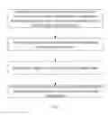
FIG. 1 is a flow chart of a method for manufacturing a multilayer FPCB;
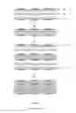
FIGS. 2 to 4 are schematic views showing a method for manufacturing a multilayer FPCB in accordance with the first embodiment;
FIG. 5 is a schematic view showing a method for manufacturing a multilayer FPCB in accordance with the second embodiment;
FIGS. 6 and 7 are schematic views showing a method for manufacturing a multilayer FPCB in accordance with the third embodiment; and
FIG. 8 is a schematic view showing a method for manufacturing a multilayer FPCB according to related art.
DETAILED DESCRIPTION OF THE PREFERRED EMBODIMENTS
FIG. 1 shows a method for manufacturing a multilayer FPCB. The method includes steps in no particular order of: providing three copper clad laminates and two binder layers, each of the copper clad laminates comprising a dielectric layer and at least one patterned conductive layer formed on the dielectric layer; stacking the copper clad laminates and the binder layers alternately one on another; laminating the at least three copper clad laminates and the at least two binder layers in one laminating step; aligning the copper clad laminates and the binder layers; and compressing the copper clad laminates and the binder layers together thereby obtaining a multilayer flexible printed circuit board.
Each steps of the method will be described in detail with the following embodiments.
As an example, the present embodiment exemplarily discloses a method for making a quadrilayer flexible printed circuit board. Referring to FIG. 2, four copper clad laminates 10, 12, 14, 16 and three binder layers 11, 13, 15 are provided. Each copper clad laminate 10 includes a dielectric layer 102, a bonding layer 104 and a conductive pattern 106. Typically, the conductive pattern 106 is made of copper, but other metals such as silver, aluminum may also be used. The bonding layer 104 bonds the conductive layer 106 and the dielectric layer 102. A positioning hole 108 can be formed in the copper clad laminate 10. The dielectric layer 102 and the binder layers 11, 13, 15 can be made of a material selected from the group consisting of polyimide, polyimide, teflon, polythiamine, polymethacrylic acid, polycarbonate, polycarbonate ester, polyester, and copolymer of imide, ethylene and dimethyl terephthate.
Referring to FIG. 3, the four copper clad laminates 10, 12, 14, 16 and the three binder layers 11, 13, 15 are stacked on a base 14 one on another in an alternating fashion. A protective layer 142 can be placed on the base 14 for preventing the lowest copper clad laminates 16 from directly contacting with the base 14. The base 14 can be a part of a laminating machine. Preferably, positioning holes 108 can be pre-formed on the copper clad laminates 10, 12, 14 and 16. The position holes can be used to align the copper clad laminates 10, 12, 14 and 16.
Referring to FIG. 4, a top plate 15 is attached to a top copper clad laminate 10 such that the four copper clad laminates 10, 12, 14, 16 are sandwiched between the top plate 150 and the base 140. Preferably, a protective layer 152 can be placed on the copper clad laminate 10 for preventing the highest copper clad laminate 10 from directly contacting with the top plate 15. A pressure P is applied between the base 140 and the top plate 150, the stacked four copper clad laminates 10, 12, 14, 16 and the three binder layers 11, 13, 15 are laminated together, thus obtaining a multilayer FPCB. During the lamination, the four copper clad laminates 10, 12, 14, 16 and the three binder layers 11, 13, 15 are heated to a temperature of about 180 to 200 degrees centigrade, and preferably to about 190 degrees centigrade. Preferably, this step includes substeps of pre-compressing the copper clad laminates and binder layers for a first period of time so as to soften the binder layers, and compressing the copper clad laminates and the binder layers for a second period of time. The binder layers 11, 13, 15 are softened due to the pressure and the elevated temperature in the pre-compressing step, and then the softened binder layers 11, 13, 15 fill all gaps in the stacked four copper clad laminates 10, 12, 14, 16 and the three binder layers 11, 13, 15 in the compressing step. Preferably, the duration of the first period of time is in the range form 5 to 15 seconds, the duration of the second period of time is in the range from 80 to 120 seconds.
According to this method, four copper clad laminates and three binder layers are stacked and laminated in one laminating step thus obtaining a multilayer FPCB with only one laminating step. Additional time consumption can be reduced and aligning precision can be increased. A possibility of short circuit on the conductive pattern can be avoided.
Referring to FIG. 5, a method for manufacturing a multilayer FPCB in accordance with the second embodiment is similar to that of the first embodiment except that two single-sided copper clad laminates 20, 22, a double-sided copper clad laminate 24 and two binder layers 21, 23 are provided, stacked and laminated. The single-sided copper clad laminate 20 includes a dielectric layer 202 and a conductive layer 204 formed on the dielectric layer 202. The single-sided copper clad laminate 22 has a similar structure with the single-sided copper clad laminate 20. The double-sided copper clad laminate 24 is similar to the single-sided copper clad laminate 20 except that includes two conductive layers.
In this embodiment, three copper clad laminates and two binder layers are stacked and laminated in one laminating step, thus obtaining a quadrilayered FPCB.
Referring to FIG. 6, a method for manufacturing a multilayer FPCB in accordance with the third embodiment is similar to that of the first embodiment except that two coverlays 36 are provided. The two coverlays 36 are disposed on two outer surfaces of the stacked copper clad laminates structure 30. As described in the second embodiment, the copper clad laminates structure 30 includes two single-side copper clad laminates, a double-sided copper clad laminate and two binder layers.
Referring to FIG. 7, the two coverlays 36 are laminated with the stacked copper clad laminates structure 30, therefore a multilayer FPCB having coverlays formed thereon is obtained by only one laminating step.
t is to be understood that the above-described embodiments are intended to illustrate rather than limit the invention. Variations may be made to the embodiments without departing from the spirit of the invention as claimed. The above-described embodiments illustrate the scope of the invention but do not restrict the scope of the invention.
Claims
What is claimed is:1. A method for manufacturing a multilayer flexible printed circuit board, the method comprising steps of:
providing three copper clad laminates and two binder layers, each of the copper clad laminates comprising a dielectric layer and at least one patterned conductive layer formed on the dielectric layer;
stacking the copper clad laminates and the binder layers one on another in alternating fashion;
aligning the copper clad laminates and the binder layers; and
compressing the copper clad laminates and the binder layers together thereby obtaining a multilayer flexible printed circuit board.
2. The method as claimed in claim 1, wherein the at least one patterned conductive layer includes two patterned conductive layers formed on opposite surfaces of the dielectric layer.
3. The method as claimed in claim 1, wherein the copper clad laminates includes at least one of a single-sided copper clad laminate, and a double-sided copper clad laminate.
4. The method as claimed in claim 1, wherein the laminating step comprises substeps of pre-compressing the copper clad laminates and binder layers for a first period of time so as to soften the binder layers, and compressing the copper clad laminates and the binder layers for a second period of time.
5. The method as claimed in claim 5, wherein the first period of time is in the range from 5 to 15 seconds.
6. The method as claimed in claim 5, wherein the second period of time is in the range from 80 to 120 seconds.
7. The method as claimed in claim 1, wherein the copper clad laminates and the binder layers are heated up to a temperature of 180 to 200 degrees centigrade during the laminating step.
8. The method as claimed in claim 1, wherein a positioning hole is defined in each of the copper clad laminates and the binder layers for facilitating alignment of the copper clad laminates.
Images & Drawings included:


Sources:
- United States Patent and Trademark Office - verify current appl. status at the USPTO↗
Similar patent applications:
- » 20080148562
Method for manufacturing multilayer flexible printed circuit board - » 20110247207
Method for manufacturing multilayer flexible printed circuit board - » 20080250637
Method for manufacturing multilayer flexible printed circuit board - » 20080116166
Method for manufacturing multilayer flexible printed circuit board - » 20140054079
MULTILAYER FLEXIBLE PRINTED CIRCUIT BOARD AND METHOD FOR MANUFACTURING SAME - » 20170280554
Method of manufacturing a multilayer flexible printed circuit board - » 20200187362
Multilayer rigid flexible printed circuit board and method for manufacturing the same - » 20110094776
Multilayer rigid flexible printed circuit board and method for manufacturing the same - » 20140008107
Multilayer rigid flexible printed circuit board and method for manufacturing the same - » 20140021164
METHOD FOR MANUFACTURING A MULTILAYER RIGID FLEXIBLE PRINTED CIRCUIT BOARD
Recent applications in this class:
- » 20240341043 2024-10-10
HIGHLY INTEGRATED POWER ELECTRONICS AND METHODS OF MANUFACTURING THE SAME - » 20240244764 2024-07-18
Method for manufacturing multi-layer flexible circuit board and article thereof - » 20230164927 2023-05-25
Method for fabricating asymmetric board - » 20230095254 2023-03-30
MULTILAYER CIRCUIT BOARD MANUFACTURING APPARATUS AND MULTILAYER CIRCUIT BOARD MANUFACTURING METHOD - » 20230092278 2023-03-23
Method of improving wire structure of circuit board and improving wire structure of circuit board - » 20220330437 2022-10-13
Method for manufacturing multi-layer flexible circuit board and article thereof - » 20210161019 2021-05-27
Method for manufacturing multilayer printed wiring board and multilayer printed wiring board - » 20190364673 2019-11-28
Printed wiring board - » 20190200463 2019-06-27
Heating of printed circuit board core during laminate cure - » 20190141841 2019-05-09
Fabricating an asymmetric printed circuit board with minimized warpage
Recent applications for this Assignee:
- » 20130092420 2013-04-18
EMBEDDED MULTILAYER PRINTED CIRCUIT BOARD AND METHOD - » 20120146277 2012-06-14
Clamping apparatus - » 20120067848 2012-03-22
Apparatus and method for wet processing substrate - » 20120055356 2012-03-08
Method for screen printing printed circuit board substrate - » 20120048603 2012-03-01
Printed circuit board - » 20120031873 2012-02-09
Etching device and method for manufacturing printed circuit board using same - » 20120018299 2012-01-26
ELECTROPLATING APPARATUS - » 20120011713 2012-01-19
Method for manufacturing multilayer printed circuit board - » 20110308082 2011-12-22
Method for manufacturing multilayer printed circuit board with plated through holes - » 20110302775 2011-12-15
Method for manufacturing printed circuit board