Method for Fabricating MRAM
US20080153178A1
2008-06-26
11/860,133
2007-09-24
Abstract:
A method of fabricating a magnetic random access memory (MRAM) is provided. A metal interconnection, a magnetic tunnel junction layer, and an interlayer dielectric layer are formed on a semiconductor substrate. A portion of the interlayer dielectric layer is selectively removed, leaving protruded regions. A metal layer is then formed on the interlayer dielectric layer and planarized using the protruded portions of the interlayer dielectric layer as a target.
Interested in similar patents?
Get notified when new applications in this technology area are published.
Classification:
H01L27/222 » CPC main
Devices consisting of a plurality of semiconductor or other solid-state components formed in or on a common substrate including components using galvano-magnetic effects, e.g. Hall effects; using similar magnetic field effects Magnetic non-volatile memory structures, e.g. MRAM
H01L43/12 » CPC further
Devices using galvano-magnetic or similar magnetic effects; Processes or apparatus specially adapted for the manufacture or treatment thereof or of parts thereof Processes or apparatus specially adapted for the manufacture or treatment of these devices or of parts thereof
H01L21/00 IPC
Processes or apparatus adapted for the manufacture or treatment of semiconductor or solid state devices or of parts thereof
Description
CROSS-REFERENCE TO RELATED APPLICATION
The present application claims the benefit under 35 U.S.C. §119 of Korean Patent Application No. 10-2006-0134064, filed Dec. 26, 2006, which is hereby incorporated by reference in its entirety.
BACKGROUND
A Magnetic Random Access Memory (MRAM) is a nonvolatile memory device, such as a flash memory device, which uses the characteristics of a magnetic member to store data.
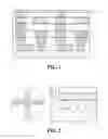
FIG. 1 is a cross-sectional view of a typical related art MRAM cell, and FIG. 2 is a top view of a wafer and a portion of a wafer including related art MRAM cells.
In general, when manufacturing MRAM cells, as shown in FIG. 1, transistors 20 are formed on a semiconductor substrate 10 and multi-layered metal interconnections 30 are connected to the transistors 20. Multi-layered interlayer dielectric layers 40 are interposed between the metal interconnections 30, digit lines 50 are formed on the final interlayer dielectric layer 40, and magnetic tunnel layers 60 are formed on the digit lines 50. Lastly, a titanium nitride (TiN) layer 70 is formed on the entire surface of the semiconductor substrate 10 including the magnetic tunnel layers 60.
The TiN layer 70 typically has a thickness of from about 400 Å to about 500 Å and a roughness equal to or less than about 5 Å.
The TiN layer 70 is often initially formed much thicker and with a roughness of about 50 Å. Then, a chemical mechanical polishing (CMP) process is performed on the TiN layer 70 to give a roughness of about 5 Å or less.
However, due to the limitations of precision in CMP equipment, a thin metal layer having a thickness of about 400 Å cannot be uniformly formed on the entire surface of the wafer. Referring to FIG. 2, the TiN layer 70 typically remains at the center portion (dotted circle) of the wafer, but is not present at the wafer edge region. This leads to the wafer having poor uniformity, partly due to over-polish. Thus, the yield rate is reduced at the wafer edge region. Also, the non-uniformity of the TiN layer 70 may cause some chips to have different characteristics depending on their positions on the wafer.
Table 1 shows the thickness of the TiN layer (Å) of four wafers according to the measurement positions X and Y shown in FIG. 2.
| TABLE 1 |
| TiN layer thickness as a function of wafer position |
| position | wafer 1 | wafer 2 | wafer 3 | wafer 4 | X | Y |
| 1 | 525 | 404 | 458 | 452 | 5.082 | 65.536 |
| 2 | 520 | 449 | 478 | 456 | 5.065 | 45.237 |
| 3 | 442 | 447 | 472 | 445 | 5.048 | 24.939 |
| 4 | 507 | 455 | 494 | 481 | 5.031 | 4.641 |
| 5 | 503 | 479 | 484 | 460 | 5.013 | −15.658 |
| 6 | 519 | 435 | 477 | 470 | 4.996 | −35.956 |
| 7 | 505 | 427 | 475 | 454 | 4.979 | −56.255 |
| 8 | Not measured | 4.962 | −76.553 |
| 9 | Not measured | −76.569 | 4.71 |
| 10 | 515 | 430 | 468 | 472 | −56.169 | 4.692 |
| 11 | 507 | 446 | 457 | 448 | −35.769 | 4.675 |
| 12 | 506 | 444 | 480 | 440 | −15.369 | 4.658 |
| 13 | 480 | 422 | 484 | 452 | 25.431 | 4.623 |
| 14 | 495 | 441 | 497 | 481 | 45.831 | 4.606 |
| 15 | 500 | 386 | 457 | 465 | 66.231 | 4.589 |
| 16 | Not measured | 86.631 | 4.572 |
| Average | 502 | 436 | 475 | 460 |
Table 1 shows that the TiN layer is not present at the edge region of the wafer since the thickness of the TiN layer cannot be measured at that region.
The method for fabricating the MRAM according to the related art represents problems as follows.
In existing MRAM devices, the TiN layer is not present at the edge region of a wafer having a plurality of the MRAM devices since over-polish occurs at the wafer edge region during the CMP process on the TiN layer. This leads to reduced yield rate and uniformity at the wafer edge region. Additionally, some chips may have different characteristics depending on the positions on the wafer.
Thus, there exists a need in the art for an improved method of forming a metal layer on an MRAM device.
BRIEF SUMMARY
Embodiments of the present invention provide a method of fabricating an MRAM cell, in which a metal layer is substantially uniformly polished during a chemical mechanical polishing (CMP) process.
A method of fabricating magnetic random access memory (MRAM) includes: forming a metal interconnection on a semiconductor substrate; forming a magnetic tunnel junction layer on the metal interconnection; forming an interlayer dielectric layer on the semiconductor substrate; planarizing the interlayer dielectric layer such that the magnetic tunnel junction layer is exposed; selectively removing a portion of the interlayer dielectric layer; forming a metal layer on the interlayer dielectric layer; and performing a planarization process on the metal layer using protruded portions of the interlayer dielectric layer as a target.
BRIEF DESCRIPTION OF THE DRAWINGS
FIG. 1 is a cross-sectional view showing a related art MRAM device.
FIG. 2 is a top view of a wafer and a portion of a wafer for a related art MRAM.
FIGS. 3 to 6 are cross-sectional views showing a method of fabricating an MRAM device according to an embodiment of the present invention.
DETAILED DESCRIPTION
When the terms “on” or “over” are used herein, when referring to layers, regions, patterns, or structures, it is understood that the layer, region, pattern or structure can be directly on another layer or structure, or intervening layers, regions, patterns, or structures may also be present. When the terms “under” or “below” are used herein, when referring to layers, regions, patterns, or structures, it is understood that the layer, region, pattern or structure can be directly under the other layer or structure, or intervening layers, regions, patterns, or structures may also be present.
FIGS. 3 to 6 are cross-sectional views showing a method of fabricating an MRAM device according to an embodiment of the present invention.
Referring to FIG. 3, a first metal layer can be deposited on a semiconductor substrate 201 having transistors (not shown). Then, the first metal layer can be selectively removed, thereby forming metal interconnections 202. In an embodiment, the first metal layer can be selectively removed through a photo process and etching process.
A magnetic tunnel junction layer 203 can be selectively formed on the metal interconnections 202. Then, an interlayer dielectric layer 204 can be formed on the semiconductor substrate 201 including the magnetic tunnel junction layer 203.
Next, a chemical mechanical polishing (CMP) process can be performed on the entire surface of the interlayer dielectric layer 204 until the upper surface of the magnetic tunnel junction layer 203 is exposed.
Then, a photoresist can be coated on the interlayer dielectric layer 204 and selectively patterned to form a photoresist pattern 205. In an embodiment, the photoresist can be patterned through an exposure and developing process.
Referring to FIG. 4, a portion of the exposed upper surface of the interlayer dielectric layer 204 can be removed. In an embodiment, the exposed interlayer dielectric layer 204 is reduced by a thickness of about 500 Å. In many embodiments, the portion of the interlayer dielectric layer is removed through a dry etching process using the photoresist pattern 205 as an etching mask.
In many embodiments, since the portions of the interlayer dielectric layer 204 under the photoresist pattern 205 are only thicker than the rest of the interlayer dielectric layer 204 by about 500 Å, the extra thickness has little effect on the insulation of the metal interconnections.
Then, the photoresist pattern 205 can be removed.
Referring to FIG. 5, a second metal layer 206 can be deposited on the entire surface of the interlayer dielectric layer 204. For example, the second metal layer can be a titanium nitride (TiN) layer. In an embodiment, the deposition thickness of the second metal layer 206 is from about 1000 Å to about 2000 Å. In one embodiment, the deposition thickness of the second metal layer 206 is about 1500 Å.
Since the portions of the interlayer dielectric layer 204 that were below the photoresist pattern 205 were not etched, those portions may be thicker than and protrude above the rest of the interlayer dielectric layer 204. Accordingly, the second metal layer 206 protrudes on the substrate 201 where the interlayer dielectric layer 204 protrudes.
Referring to FIG. 6, a CMP process can be performed on the entire surface of the second metal layer 206 using the protruded portions of the upper surface of the interlayer dielectric layer 204 as a target. In an embodiment, the second metal layer 206 can have about 1000 Å polished away through the CMP process, such that a second metal layer 206 that was deposited with a thickness of about 1500 Å would have a thickness of about 500 Å after the CMP process.
As stated above, in an embodiment, the second metal layer can be a TiN layer. Due to the characteristics of metal slurry that can be used in the CMP process, the selectivity between TiN and the interlayer dielectric layer 204 can be about 50:1. Thus, a TiN layer can be uniformly over the whole area of the wafer, even if the wafer is over-polished.
Embodiments of the present invention provide portions of the interlayer dielectric layer 204 that protrude from the top surface of the interlayer dielectric layer, thereby allowing the second metal layer to be uniformly formed over the whole area of a wafer. The second metal layer, such as a TiN layer, can be uniformly formed even if a CMP process is performed after the second metal layer has been deposited.
Any reference in this specification to “one embodiment,” “an embodiment,” “example embodiment,” etc., means that a particular feature, structure, or characteristic described in connection with the embodiment is included in at least one embodiment of the invention. The appearances of such phrases in various places in the specification are not necessarily all referring to the same embodiment. Further, when a particular feature, structure, or characteristic is described in connection with any embodiment, it is submitted that it is within the purview of one skilled in the art to effect such feature, structure, or characteristic in connection with other ones of the embodiments.
Although embodiments have been described with reference to a number of illustrative embodiments thereof, it should be understood that numerous other modifications and embodiments can be devised by those skilled in the art that will fall within the spirit and scope of the principles of this disclosure. More particularly, various variations and modifications are possible in the component parts and/or arrangements of the subject combination arrangement within the scope of the disclosure, the drawings and the appended claims. In addition to variations and modifications in the component parts and/or arrangements, alternative uses will also be apparent to those skilled in the art.
Claims
What is claimed is:1. A method of fabricating a magnetic random access memory (MRAM), comprising:
forming a metal interconnection on a semiconductor substrate;
forming a magnetic tunnel junction layer on the metal interconnection;
forming an interlayer dielectric layer on the semiconductor substrate including the metal interconnection and magnetic tunnel junction layer;
planarizing the interlayer dielectric layer such that a top surface of the magnetic tunnel junction layer is exposed;
removing a portion of the interlayer dielectric layer, resulting in at least one protruded portion of the interlayer dielectric layer;
forming a metal layer on the interlayer dielectric layer having the at least one protruded portion; and
planarizing the metal layer using the at least one protruded portion of the interlayer dielectric layer as a target.
2. The method according to claim 1, wherein removing a portion of the interlayer dielectric layer comprises:
depositing a photoresist on the interlayer dielectric layer;
patterning the photoresist through an exposure and developing process to form a photoresist pattern;
performing a dry etching process on the interlayer dielectric layer using the photoresist pattern as an etching mask; and
removing the photoresist pattern.
3. The method according to claim 1, wherein planarizing the interlayer dielectric layer comprises performing a chemical mechanical polishing (CMP) process.
4. The method according to claim 1, wherein planarizing the metal layer comprises performing a CMP process.
5. The method according to claim 1, wherein the metal layer comprises titanium nitride (TiN).
6. The method according to claim 1, wherein the forming a metal layer comprises depositing the metal layer to a thickness of from about 1000 Å to about 2000 Å.
7. The method according to claim 6, wherein the forming a metal layer comprises depositing the metal layer to a thickness of about 1500 Å.
8. The method according to claim 1, wherein the at least one protruded portion of the interlayer dielectric layer protrudes to about 500 Å above a non-protruded portion of the interlayer dielectric layer.
9. The method according to claim 1, wherein after the metal layer is planarized, the metal layer has a thickness of about 500 Å.
Images & Drawings included:


Sources:
- United States Patent and Trademark Office - verify current appl. status at the USPTO↗
Similar patent applications:
- » 20130267042
MRAM fabrication method with sidewall cleaning - » 20110089507
Bit line preparation method in MRAM fabrication - » 20060172439
Method of fabricating MRAM cells - » 20240423093
METHODS FOR FABRICATING MRAM WITH VOID FREE INTERLAYER DIELECTRIC - » 20170018707
Method for fabricating MRAM bits on a tight pitch - » 20090173977
Method of MRAM fabrication with zero electrical shorting - » 20190157548
Via structure, MRAM device using the via structure and method for fabricating the MRAM device - » 20150008546
MRAM device and fabrication method thereof - » 20130049144
Magnetoresistive random access memory (MRAM) device and fabrication methods thereof - » 20050214953
Method of fabricating a MRAM device
Recent applications in this class:
- » 20230371275 2023-11-16
METHOD OF FORMING DIFFERENT TYPES OF MEMORY DEVICES - » 20230262992 2023-08-17
MRAM INTERCONNECT INTEGRATION WITH SUBTRACTIVE METAL PATTERNING - » 20230240080 2023-07-27
Multiferroic memory with piezoelectric layers and related methods - » 20230232637 2023-07-20
Magnetic memory device and method for forming the same - » 20230200087 2023-06-22
SEMICONDUCTOR DEVICE - » 20230200086 2023-06-22
Magneto-resistive random access memory with substitutional bottom electrode - » 20230189535 2023-06-15
Magneto-resistive random access memory with segmented bottom electrode - » 20230189534 2023-06-15
LAYERED BOTTOM ELECTRODE DIELECTRIC FOR EMBEDDED MRAM - » 20230157032 2023-05-18
BIT-LINE RESISTANCE REDUCTION - » 20230139618 2023-05-04
SEMICONDUCTOR DEVICES