SEMICONDUCTOR DEVICE AND FABRICATING METHOD THEREOF
US20080157366A1
2008-07-03
11/954,197
2007-12-11
Abstract:
A semiconductor device and fabricating method thereof are disclosed. Embodiments relate to forming metal lines having a prescribed pattern over a lower insulating interlayer, forming a silicon oxide layer over surfaces of the metal lines and a surface of the lower insulating interlayer exposed between the metal lines, and forming an upper insulating interlayer over the silicon oxide layer.
Interested in similar patents?
Get notified when new applications in this technology area are published.
Classification:
H01L23/5329 » CPC main
Details of semiconductor or other solid state devices; Arrangements for conducting electric current within the device in operation from one component to another, i.e. interconnections, e.g. wires, lead frames including external interconnections consisting of a multilayer structure of conductive and insulating layers inseparably formed on the semiconductor body characterised by the materials Insulating materials
H01L21/76834 » CPC further
Processes or apparatus adapted for the manufacture or treatment of semiconductor or solid state devices or of parts thereof; Manufacture or treatment of devices consisting of a plurality of solid state components formed in or on a common substrate or of parts thereof; Manufacture of integrated circuit devices or of parts thereof; Manufacture of specific parts of devices defined in group; Applying interconnections to be used for carrying current between separate components within a device comprising conductors and dielectrics characterised by the formation and the after-treatment of the dielectrics, e.g. smoothing characterised by the formation of thin functional dielectric layers, e.g. dielectric etch-stop, barrier, capping or liner layers formation of thin insulating films on the sidewalls or on top of conductors
H01L21/76837 » CPC further
Processes or apparatus adapted for the manufacture or treatment of semiconductor or solid state devices or of parts thereof; Manufacture or treatment of devices consisting of a plurality of solid state components formed in or on a common substrate or of parts thereof; Manufacture of integrated circuit devices or of parts thereof; Manufacture of specific parts of devices defined in group; Applying interconnections to be used for carrying current between separate components within a device comprising conductors and dielectrics characterised by the formation and the after-treatment of the dielectrics, e.g. smoothing Filling up the space between adjacent conductive structures; Gap-filling properties of dielectrics
H01L23/53295 » CPC further
Details of semiconductor or other solid state devices; Arrangements for conducting electric current within the device in operation from one component to another, i.e. interconnections, e.g. wires, lead frames including external interconnections consisting of a multilayer structure of conductive and insulating layers inseparably formed on the semiconductor body characterised by the materials; Insulating materials Stacked insulating layers
H01L2924/0002 » CPC further
Indexing scheme for arrangements or methods for connecting or disconnecting semiconductor or solid-state bodies as covered by; Technical content checked by a classifier Not covered by any one of groups , and
H01L2924/00 » CPC further
Indexing scheme for arrangements or methods for connecting or disconnecting semiconductor or solid-state bodies as covered by
H01L23/48 IPC
Details of semiconductor or other solid state devices Arrangements for conducting electric current to or from the solid state body in operation, e.g. leads, terminal arrangements ; Selection of materials therefor
H01L21/44 IPC
Processes or apparatus adapted for the manufacture or treatment of semiconductor or solid state devices or of parts thereof; Manufacture or treatment of semiconductor devices or of parts thereof the devices having at least one potential-jump barrier or surface barrier, e.g. PN junction, depletion layer or carrier concentration layer the devices having semiconductor bodies not provided for in groups, , , and with or without impurities, e.g. doping materials Manufacture of electrodes on semiconductor bodies using processes or apparatus not provided for in groups -
Description
The present application claims priority under 35 U.S.C. 119 to Korean Patent Application No. 10-2006-0137279, filed on Dec. 29, 2006, which is hereby incorporated by reference in its entirety.
BACKGROUND
In a semiconductor fabricating process, a metal line may be formed by depositing a metal layer. The layer may be coated with photoresist, which is developed to form a photoresist pattern. A metal pattern is formed by etching the metal layer. An oxide layer of SiO2 may then be deposited by HDP (high density plasma). In the metal layer depositing step, there may be particles on the metal, and it may be difficult to etch a specific pattern. An abnormal metal line may be formed with a protrusion defect.
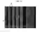
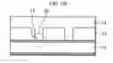
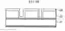
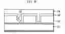
FIG. 1A and FIG. 1B show problems in a semiconductor device fabricating method according to the related art. FIG. 1A is a SEM picture of a metal line layout and FIG. 1B is a cross-sectional diagram. Referring to FIG. 1A and FIG. 1B, when metal lines 12 are formed on a lower insulating interlayer 11, if a stray particle lies in a gap between the metal lines 12, the subsequent etch may not be successfully performed, and a protrusion defect 13 may occur. Subsequently, in depositing an upper insulating interlayer 14 which fills the gap between the metal lines 12, the area with the protrusion defect 13 may not be correctly filled up with the oxide insulator. This may result in the formation of a void 15. As semiconductor devices become more highly integrated, the metal lines 12 become more ultra-microscopic. If a protrusion defect 13 is generated, the gap between the metal lines 12 gets narrower. Thus, it is difficult to achieve a complete filling of the gap between metal lines. When thermal stresses are applied to the defect region by an EM (electro-migration) test and/or an EFR (early failure rate) test, the void causes the metal lines to fail. An inter-metal bridge may be generated, which degrades reliability of device.
SUMMARY
Embodiments relate to semiconductor device fabrication, and more particularly, to a semiconductor device and fabricating method thereof. Embodiments relate to preventing a bridge effect between metal lines by having a gap between ultra-microscopic metal lines filled up with an insulating interlayer.
Embodiments relate to a semiconductor device and fabricating method thereof, by which a gap between metal lines of the semiconductor device can be completely filled up with an insulating interlayer. Embodiments relate to semiconductor devices and fabricating methods in which inter-metal-line bridges can be prevented when thermal stresses are applied to the semiconductor devices. Embodiments relate to semiconductor devices and fabrication methods by which fault resistance to any applied thermal stresses, including EM and/or EFR tests, are improved to enhance reliability.
Embodiments relate to a method of fabricating a semiconductor device by forming metal lines having a prescribed pattern over a lower insulating interlayer. A silicon oxide layer may be formed over surfaces of the metal lines and a surface of the lower insulating interlayer exposed between the metal lines. An upper insulating interlayer may be formed over the silicon oxide layer. The relatively thin silicon oxide layer may be formed on the surface of the insulating interlayer using ozone-tetraethoxysilane (O3-TEOS). The silicon oxide layer may be formed by atomic layer deposition.
The silicon oxide layer forming step may include the steps of introducing TEOS using inert gas as a carrier, performing pumping until a base pressure is reached, and introducing O3.
The TEOS introducing step may be performed while a pressure below 10 Torr is maintained at 300˜400° C. And, the silicon oxide layer forming step may be repeated until a thickness of an O3-TEOS insulating layer as the silicon oxide layer reaches 300˜500 Å.
The upper insulating interlayer may include a USG layer and a d-TEOS layer.
The upper insulating interlayer may be formed by high density plasma deposition.
Embodiments relate to a semiconductor device includes metal lines having a prescribed pattern over a lower insulating interlayer, a silicon oxide layer over surfaces of the metal lines and a surface of the lower insulating interlayer exposed between the metal lines, and an upper insulating interlayer over the silicon oxide layer.
The silicon oxide layer may include an O3-TEOS insulating layer.
DRAWINGS
FIG. 1A and FIG. 1B are diagrams to explain a problem of a semiconductor device fabricating method according to a related art.
Example FIGS. 2A to 2C are cross-sectional diagrams of a semiconductor device and fabricating method thereof according to embodiments.
Example FIGS. 3A to 3C are cross-sectional diagrams of a semiconductor device and fabricating method thereof according to embodiments.
DESCRIPTION
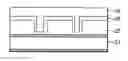
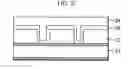
Example FIGS. 2A to 2C are cross-sectional diagrams of a semiconductor device and fabricating method thereof according to embodiments. Referring to example FIG. 2A, metal lines 22 having a prescribed pattern are formed over a lower insulating interlayer 21. The metal lines 22 may be formed by a metal line forming process technique such as reactive ion etch (RIE).
Referring to example FIG. 2B, a relatively thin O3-TEOS insulating layer 26 is formed over surfaces of the metal lines 22 and surfaces of the lower insulating interlayer 21 exposed between the metal lines 22. The O3-TEOS insulating layer 26 may be formed by ALD (atomic layer deposition). Details of an example of the formation of the O3-TEOS insulating layer 26 are explained below.
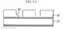
TEOS (tetra ethyl orthosilicate) may be introduced into a chamber using inert gas such as He as a carrier. The pressure may be maintained below approximately 10 Torr and the temperature may be maintained at approximately 300˜400° C. After the TEOS introduction, pumping is carried out until a base pressure is reached. O3 is then introduced into the chamber. Oxygen (O) dissociated from O3 causes decomposition of the adsorbed TEOS to reconfigure Si—O—Si or Si—O—H. Thus, the O3-TEOS insulating layer 26 of silicon oxide grows. The growth thickness of the O3-TEOS insulating layer 26 corresponds to several angstroms (Å). After the introduction of O3 has been stopped, pumping is carried out to reach the base pressure again. The above steps may be repeated from the TEOS introducing step until the thickness of the O3-TEOS insulating layer 26 reaches approximately 300˜500 Å.
The method of forming the O3-TEOS insulating layer 26 explained above grows a silicon oxide layer by the repetition of TEOS surface adsorption and dissolution. Hence, the microscopic gap between the metal lines 22 may be completely filled up with the silicon oxide layer. Since probability of adsorption is equal across the whole surface, complete filling of gaps between the metal lines can be expected.
Referring to example FIG. 2C, an upper insulating interlayer 24 is deposited over the O3-TEOS insulating layer 26. The upper insulating interlayer 24 includes a USG (undoped silicate glass) layer of about 3000 Å and a d-TEOS layer of about 6,000 Å. The deposition of the upper insulating interlayer 24 may be carried out using a high-density plasma process.
Thus, if the upper insulating interlayer 24 is deposited after completion of the O3-TEOS insulating layer 26, the gap between the ultra-microscopic metal lines 22 having a protrusion defect therein can be completely filled up with the upper insulating interlayer 24. This is explained in the following description.
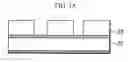
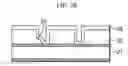
Example FIGS. 3A to 3C are cross-sectional diagrams of a semiconductor device and fabricating method thereof according to embodiments. If a protrusion defect 23, as shown in example FIG. 3A, occurs in a gap between metal lines 22, a relatively thin O3-TEOS insulating layer 26, as shown in example FIG. 3B, may be formed by atomic layer deposition. Subsequently, an upper insulating interlayer 24, as shown in example FIG. 3C, may be deposited over the O3-TEOS insulating layer 24. Therefore, the gap between the ultra-microscopic metal lines 22 having a protrusion defect 23 can be completely filled up with the insulating interlayer 24.
After metal lines have been formed, a relatively thin O3-TEOS insulating layer may be formed by atomic layer deposition before forming an insulating interlayer. Hence, a gap between the ultra-microscopic metal lines can be completely filled up with the insulating interlayer.
Even if a thermal stress is applied to a semiconductor device, the embodiments prevent an inter-metal-line bridge effect. Hence, the embodiments improve EM and EFR characteristics, thereby enhancing device reliability.
It will be obvious and apparent to those skilled in the art that various modifications and variations can be made in the embodiments disclosed. Thus, it is intended that the disclosed embodiments cover the obvious and apparent modifications and variations, provided that they are within the scope of the appended claims and their equivalents.
Claims
What is claimed is:1. A method comprising:
forming metal lines having a prescribed pattern over a lower insulating interlayer;
forming a silicon oxide layer over surfaces of the metal lines and surfaces of the lower insulating interlayer exposed between the metal lines; and
forming an upper insulating interlayer over the silicon oxide layer.
2. The method of claim 1, wherein the silicon oxide is a relatively thin layer formed over the surface of the insulating interlayer.
3. The method of claim 1, wherein the silicon oxide layer is formed using O3-TEOS.
4. The method of claim 1, wherein the silicon oxide layer is formed by atomic layer deposition.
5. The method of claim 1, wherein forming the silicon oxide layer comprises:
introducing TEOS using inert gas as a carrier;
pumping until a base pressure is reached; and
introducing O3.
6. The method of claim 5, wherein the TEOS is introduced at a pressure maintained below approximately 10 Torr.
7. The method of claim 6, wherein the TEOS is at a temperature of approximately 300° C. to 400° C.
8. The method of claim 5, wherein forming the silicon oxide layer is repeated until a thickness of an O3-TEOS insulating layer reaches approximately 300 Å to 500 Å.
9. The method of claim 1, wherein the upper insulating interlayer comprises a undoped silicate glass layer.
10. The method of claim 1, wherein the upper insulating interlayer comprises a d-TEOS layer.
11. The method of claim 1, wherein the upper insulating interlayer is formed by high density plasma deposition.
12. A semiconductor device, comprising:
metal lines having a prescribed pattern over a lower insulating interlayer;
a silicon oxide layer formed over surfaces of the metal lines and a surface of the lower insulating interlayer exposed between the metal lines; and
an upper insulating interlayer formed over the silicon oxide layer.
13. The semiconductor device of claim 9, wherein the silicon oxide layer comprises an O3-TEOS insulating layer.
14. An apparatus comprising:
metal lines formed having a prescribed pattern over a lower insulating interlayer;
a silicon oxide layer formed over surfaces of the metal lines and surfaces of the lower insulating interlayer exposed between the metal lines; and
an upper insulating interlayer formed over the silicon oxide layer.
15. The apparatus of claim 14, wherein the silicon oxide is a relatively thin layer of O3-TEOS formed over the surface of the insulating interlayer.
16. The apparatus of claim 14, wherein the silicon oxide layer is formed by atomic layer deposition.
17. The apparatus of claim 14, wherein the silicon oxide layer is formed by:
introducing TEOS using inert gas as a carrier;
pumping until a base pressure is reached; and
introducing O3.
18. The apparatus of claim 17, wherein TEOS is introduced at a pressure maintained below approximately 10 Torr and at a temperature of approximately 300° C. to 400° C.
19. The apparatus of claim 17, wherein the silicon oxide layer is formed from O3-TEOS to have a thickness of approximately 300 Å to 500 Å.
20. The apparatus of claim 14, wherein the upper insulating interlayer comprises an undoped silicate glass layer.
Images & Drawings included:
Sources:
- United States Patent and Trademark Office - verify current appl. status at the USPTO↗
Similar patent applications:
- » 20050032339
Substrate of semiconductor device and fabrication method thereof as well as semiconductor device and fabrication method thereof - » 20160233155
Semiconductor device, fabricating method thereof and semiconductor package including the semiconductor device - » 20120133048
Semiconductor device, fabricating method thereof and semiconductor package including the semiconductor device - » 20140057430
Semiconductor device, fabricating method thereof and semiconductor package including the semiconductor device - » 20160155937
Vertical type semiconductor device, fabrication method thereof and operation method thereof - » 20160155498
Vertical type semiconductor device, fabrication method thereof and operation method thereof - » 20060246359
Semiconductor device, fabricating method thereof, and photomask - » 20100019241
SEMICONDUCTOR DEVICE, FABRICATION METHOD THEREOF, AND PHOTOMASK - » 20140254256
Vertical type semiconductor device, fabrication method thereof and operation method thereof - » 20210280563
SEMICONDUCTOR DEVICE, FABRICATION METHOD THEREOF, PACKAGE AND FABRICATION METHOD THEREOF
Recent applications in this class:
- » 20250174563 2025-05-29
Transistor Device - » 20250157933 2025-05-15
SEMICONDUCTOR DEVICE AND METHOD FOR MANUFACTURING THE SEMICONDUCTOR DEVICE - » 20250125267 2025-04-17
SEMICONDUCTOR HAVING A FUNCTIONAL PROTECTION STRUCTURE AND METHOD OF MANUFACTURE - » 20250079315 2025-03-06
SEMICONDUCTOR STRUCTURE AND METHOD FOR FORMING THE SAME - » 20250070028 2025-02-27
INTERCONNECTION STRUCTURE WITH COMPOSITE ISOLATION FEATURE AND METHOD FOR MANUFACTURING THE SAME - » 20250070027 2025-02-27
METHOD OF FORMING AN INTERCONNECT STRUCTURE HAVING AN AIR GAP AND STRUCTURE THEREOF - » 20250062234 2025-02-20
SEMICONDUCTOR STRUCTURE AND METHOD FOR MANUFACTURING SAME - » 20250054866 2025-02-13
INTERCONNECT STRUCTURE AND ELECTRONIC DEVICE INCLUDING THE SAME - » 20250046717 2025-02-06
Microelectronic Devices with Good Reliability and Related Compositions and Methods - » 20240429170 2024-12-26
SEMICONDUCTOR DEVICE AND METHOD FOR MANUFACTURING SEMICONDUCTOR DEVICE