Transparent thin film transistor, and method of manufacturing the same
US20080166475A1
2008-07-10
11/763,373
2007-06-14
✅ Patent granted
US 8,698,215 B2
2014-04-15
-
-
Kimberly Rizkallah | Duy T Nguyen
Christie, Parker & Hale, LLP
2031-07-28
Abstract:
A thin film transistor (TFT) and a method of manufacturing the same such that an ohmic contact can be formed between a semiconductor layer and a source electrode or between the semiconductor layer and a drain electrode, wherein the TFT can be applied to a plastic substrate. The TFT includes: a substrate; an active layer formed of ZnO, InZnO, ZnSnO, and/or ZnInGaO on the substrate and including a channel region, a source region, and a drain region; a gate electrode insulated from the active layer; and source and drain electrodes insulated from the gate electrode and electrically connected to the source region and the drain region, respectively, wherein the source region and the drain region of the active layer include hydrogen.
Inventors:
- Hyun-Soo SHIN 22 🇰🇷 Suwon-si, South Korea
- Yeon-Gon MO 44 🇰🇷 Suwon-si, South Korea
- Jae-Kyeong JEONG 31 🇰🇷 Suwon-si, South Korea
Assignee:
- SAMSUNG DISPLAY CO., LTD. 15,004 🇰🇷 Yongin-si, South Korea
Applicant:
Interested in similar patents?
Get notified when new applications in this technology area are published.
Classification:
H01L27/127 » CPC main
Devices consisting of a plurality of semiconductor or other solid-state components formed in or on a common substrate including semiconductor components specially adapted for rectifying, oscillating, amplifying or switching and having at least one potential-jump barrier or surface barrier; including integrated passive circuit elements with at least one potential-jump barrier or surface barrier the substrate being other than a semiconductor body, e.g. an insulating body comprising a plurality of TFTs formed on a non-semiconducting substrate, e.g. driving circuits for AMLCDs; Multistep manufacturing methods with a particular formation, treatment or patterning of the active layer specially adapted to the circuit arrangement
H01L27/1218 » CPC further
Devices consisting of a plurality of semiconductor or other solid-state components formed in or on a common substrate including semiconductor components specially adapted for rectifying, oscillating, amplifying or switching and having at least one potential-jump barrier or surface barrier; including integrated passive circuit elements with at least one potential-jump barrier or surface barrier the substrate being other than a semiconductor body, e.g. an insulating body comprising a plurality of TFTs formed on a non-semiconducting substrate, e.g. driving circuits for AMLCDs with a particular composition or structure of the substrate
H01L27/1225 » CPC further
Devices consisting of a plurality of semiconductor or other solid-state components formed in or on a common substrate including semiconductor components specially adapted for rectifying, oscillating, amplifying or switching and having at least one potential-jump barrier or surface barrier; including integrated passive circuit elements with at least one potential-jump barrier or surface barrier the substrate being other than a semiconductor body, e.g. an insulating body comprising a plurality of TFTs formed on a non-semiconducting substrate, e.g. driving circuits for AMLCDs with a particular composition, shape or crystalline structure of the active layer with semiconductor materials not belonging to the group IV of the periodic table, e.g. InGaZnO
B05D5/12 IPC
Processes for applying liquids or other fluent materials to surfaces to obtain special surface effects, finishes or structures to obtain a coating with specific electrical properties
H01L29/76 IPC
Semiconductor devices adapted for rectifying, amplifying, oscillating or switching, or capacitors or resistors with at least one potential-jump barrier or surface barrier, e.g. PN junction depletion layer or carrier concentration layer; Details of semiconductor bodies or of electrodes thereof; Multistep manufacturing processes therefor; Types of semiconductor device ; Multistep manufacturing processes therefor controllable by only the electric current supplied, or only the electric potential applied, to an electrode which does not carry the current to be rectified, amplified or switched Unipolar devices, e.g. field effect transistors
Description
CROSS-REFERENCE TO RELATED PATENT APPLICATION
This application claims priority to and the benefit of Korean Patent Application No. 10-2007-0002172, filed on Jan. 8, 2007, in the Korean Intellectual Property Office, the entire content of which is incorporated herein by reference.
BACKGROUND OF THE INVENTION
1. Field of the Invention
The present invention relates to a thin film transistor (TFT) and a method of manufacturing the same.
2. Description of the Related Art
A thin film transistor (TFT) is a transistor that uses a semiconductor material as an active layer. Recently, research is being conducted on TFTs that are included in a pixel area of a flat display device, such as an organic light emitting display device, so that light can pass through a TFT and be output to the outside.
Conventionally, the electrical contact between a source electrode and a semiconductor layer of a TFT, or between a drain electrode and the semiconductor layer of the TFT is an important factor for defining the characteristics of the TFT. Accordingly, in a conventional silicon TFT using a silicon semiconductor layer as an active layer, the silicon semiconductor layer is doped to increase the electrical contact (e.g., to decrease a resistance ohmic contact) between the source electrode and the silicon semiconductor layer, or between the drain electrode and the silicon semiconductor layer, thereby improving the characteristics of the conventional silicon TFT.
However, as discussed above, research is being conducted on a TFT using a semiconductor material as an active layer that can be applied to a structure in which light can pass through the TFT that is included in a display unit so that the light is output to the outside. In such TFT, the electrical contact between the source electrode and the active layer or between the drain electrode and an active layer should be further increased.
In a TFT, an oxide semiconductor can provide a relatively low resistance ohmic contact (of 10−5 Ωcm2 or less) that is formed between the oxide semiconductor and the source and drain electrodes. To this end, a dopant such as Ga or Al may be applied through an ion injection process such as silicon doping; however, the temperature of the activation process in this case is 500° C. or higher. Thus, due to this high temperature, the oxide semiconductor cannot be applied to a plastic substrate in order to realize a flexible flat display device.
SUMMARY OF THE INVENTION
An aspect of an embodiment of the present invention is directed to a thin film transistor (TFT) and a method of manufacturing the same such that an ohmic contact can be formed between source and drain electrodes and a semiconductor layer, and the TFT can be applied to a plastic substrate.
An aspect of an embodiment of the present invention is directed to a TFT and a method of manufacturing the same such that an ohmic contact can be formed between source and drain electrodes and an active layer
According to an embodiment of the present invention, there is provided a thin film transistor (TFT) including: a substrate; an active layer disposed on the substrate and having a channel region, a source region, and a drain region, the active layer including a material selected from the group consisting of ZnO, InZnO, ZnSnO, and ZnInGaO; a gate electrode insulated from the active layer; a source electrode insulated from the gate electrode and electrically connected to the source region of the active layer; and a drain electrode insulated from the gate electrode and electrically connected to the drain region of the active layer, wherein the source region and the drain region of the active layer include hydrogen.
In one embodiment, a concentration of hydrogen of the source region and the drain region of the active layer ranges from about 1018/cm3 to about 1021/cm3.
In one embodiment, the substrate is a plastic substrate.
In one embodiment, the active layer is transparent to light.
In one embodiment, the TFT further includes a gate insulating layer disposed on the active layer to be between the gate electrode and the active layer, wherein the gate electrode is disposed on the gate insulating layer.
According to another embodiment of the present invention, there is provided a TFT including: a substrate; a gate electrode disposed on the substrate; an active layer including a material selected from the group consisting of ZnO, InZnO, ZnSnO, and ZnInGaO and insulated from the gate electrode, the active layer having a channel region, a source region, and a drain region; a source electrode insulated from the gate electrode and electrically connected to the source region of the active layer; and a drain electrode insulated from the gate electrode and electrically connected to the drain region of the active layer, wherein the source region and the drain region of the active layer include hydrogen.
In one embodiment, a concentration of hydrogen of the source region and the drain region of the active layer ranges from about 1018/cm3 to about 1021/cm3.
In one embodiment, the substrate is a plastic substrate.
In one embodiment, the active layer is transparent to light.
In one embodiment, the TFT further includes a gate insulating layer disposed on the active layer to be between the gate electrode and the active layer, wherein the gate electrode is disposed on the gate insulating layer.
According to another embodiment of the present invention, there is provided a method of manufacturing a thin film transistor (TFT). The method includes: forming an active layer on a substrate using a material selected from the group consisting of ZnO, InZnO, ZnSnO, and ZnInGaO, the active layer having a channel region, a source region, and a drain region; forming a gate insulating layer to cover the active layer; forming a gate electrode on the gate insulating layer; implanting hydrogen ions on the gate insulating layer in order to inject hydrogen into the source region and the drain region of the active layer; and forming a source electrode and a drain electrode to be electrically connected to the source region and the drain region of the active layer, respectively.
In one embodiment, during the implanting of the hydrogen ions, a hydrogen ion dose ranges from about 1 e16/cm2 to about 1 e18/cm2.
In one embodiment, during the implanting of the hydrogen ions, an injection energy of the hydrogen ions ranges from about 50 keV to about 150 keV.
In one embodiment, the method further comprises heat treating the active layer after the implanting of the hydrogen ions.
In one embodiment, the heat treating of the active layer after the implanting of the hydrogen ions includes heat treating the active layer at a temperature of about 200° C.
According to another embodiment of the present invention, there is provided a method of manufacturing a thin film transistor (TFT). The method includes: forming a gate electrode on a substrate; forming a gate insulating layer to cover the gate electrode; forming an active layer comprising a channel region, a source region, and a drain region on the gate insulating layer using a material selected from the group consisting of ZnO, InZnO, ZnSnO, and ZnInGaO; forming an interlayer insulating layer to cover the active layer; implanting hydrogen ions into the interlayer insulating layer to inject hydrogen ions into the source region and the drain region of the active layer; and forming a source electrode and a drain electrode to be electrically connected to the source region and the drain region of the active layer, respectively.
In one embodiment, during the implanting of the hydrogen ions, a hydrogen ion dose ranges from about 1 e16/cm2 to about 1 e18/cm2.
In one embodiment, during the implanting of the hydrogen ions, an injection energy of the hydrogen ions ranges from about 50 keV to about 150 keV.
In one embodiment, the method further comprises heat treating the active layer after the implanting of the hydrogen ions.
In one embodiment, the heat treating of the active layer after the implanting of the hydrogen ions includes heat treating the active layer at a temperature of about 200° C.
BRIEF DESCRIPTION OF THE DRAWINGS
The accompanying drawings, together with the specification, illustrate exemplary embodiments of the present invention, and, together with the description, serve to explain the principles of the present invention.
FIGS. 1A, 1B, 1C, 1D, 1E, 1F, and 1G are cross-sectional views illustrating a method of manufacturing a thin film transistor (TFT) according to an embodiment of the present invention; and
FIGS. 2A, 2B, 2C, 2D, 2E, 2F, 2G, and 2H are cross-sectional views illustrating a method of manufacturing a TFT according to another embodiment of the present invention.
DETAILED DESCRIPTION
In the following detailed description, only certain exemplary embodiments of the present invention have been shown and described, simply by way of illustration. As those skilled in the art would realize, the described embodiments may be modified in various different ways, all without departing from the spirit or scope of the present invention. Accordingly, the drawings and description are to be regarded as illustrative in nature and not restrictive. In addition, when an element is referred to as being “on” another element, it can be directly on the another element or be indirectly on the another element with one or more intervening elements interposed therebetween. Hereinafter, like reference numerals refer to like elements,
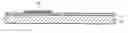
FIGS. 1A through 1G are cross-sectional views illustrating a method of manufacturing a thin film transistor (TFT) according to an embodiment of the present invention.
First, as illustrated in FIG. 1A, an active layer 12 is formed on a buffer layer 11 that is formed on a substrate 10. The substrate 10 may be glass or other various plastic substrates such as acryl. When a TFT is formed on the substrate 10 and a display device is formed on the TFT such that light passes through the TFT and is output to the outside, a transparent substrate may be used. Alternatively, a reflective substrate such as metal may be used as the substrate 10 after forming a TFT on the substrate 10 and a display device on the TFT. In this case, various suitable modifications depending on various purposes can be made, for example, a modification can be made such that light passes through the TFT between the display device and the substrate to enable optical resonance.
A patterned active layer 12 is formed on the buffer layer 11. The patterned active layer 12 may be formed of a semiconductor oxide, specifically, of a material including ZnO such as ZnO, InZnO, ZnSnO or ZnInGaO. However, the present invention is not limited thereto, and other materials having characteristics of a semiconductor can be used to form the patterned active layer 12. The patterned active layer 12 can be formed in a pattern as illustrated in FIG. 1A by using a deposition method using a mask or by forming a semiconductor material corresponding to the entire upper surface of the substrate 10 and then patterning the semiconductor material.
After forming the patterned active layer 12, a gate insulating layer 13 is formed on the active layer 12 and the buffer layer 11 as illustrated in FIG. 1B.
The gate insulating layer 13 can be formed using various suitable materials such as an organic material like parylene or epoxy having insulation characteristics. Also the gate insulating layer 13 may be formed of an inorganic material, and if the gate insulating layer 13 needs to be relatively dense, the gate insulating layer 13 may be formed using silicon oxide or silicon nitride.
Then, a gate electrode 14 and a bottom electrode 15a of a capacitor 15 are formed on the gate insulating layer 13 as illustrated in FIG. 1C. The gate electrode 14 and the bottom electrode 15a of the capacitor may be formed of a conductive material such as Al, Mo, W, Cr, Ni or compounds thereof. In one embodiment, if light needs to pass through other elements besides the active layer 12 of the TFT, the gate electrode 14 and the bottom electrode 15a of the capacitor 15 may be formed using various transparent conductive materials such as indium tin oxide (ITO) and/or indium zinc oxide (IZO). The gate electrode 14 and the bottom electrode 15a of the capacitor 15 can be formed as a single layer structure or a multi-layer structure.
After forming the gate electrode 14, hydrogen ions can be implanted into the active layer 12 using the gate electrode 14 as a self-aligned mask as illustrated in FIG. 1D. Then, as the gate electrode 14 covers a channel region of the active layer 12, a source region 12b and a drain region 12c of the active layer 12 can be doped with ions while hydrogen ions are implanted as illustrated in FIG. 1E.
In one embodiment of the present embodiment, the hydrogen ion dose is in the range from 1 e16/cm2 to 1 e18/cm2, and the hydrogen ion injection energy is between 50 keV to 150 keV. In one embodiment, when the hydrogen ion dose is lower than 1 e16/cm2, the improvement of contact resistance is low. In another embodiment, when the hydrogen ion dose is higher than 1 e18/cm2, the solubility limit is exceeded, thereby reducing doping efficiency. In one embodiment, when the hydrogen ion injection energy is lower than 50 keV, the injection depth of the dose from the surface is decreased. In another embodiment, when the hydrogen ion injection energy is higher than 150 keV, the cost of a suitable ion injection equipment increases.
Accordingly, as illustrate in FIG. 1E, the source region 12b and the drain region 12c of the active layer 12 can be made of n+ layer for forming an ohmic contact.
Accordingly, the hydrogen concentration of the source region 12b and the drain region 12c of the active layer 12 may be set to be in the range from 1018/cm3 to 1021/cm3. In one embodiment, when the hydrogen concentration of the source region 12b and the drain region 12c of the active layer 12 is lower than 1018/cm3, the improvement of contact resistance is low. In another embodiment, when the hydrogen concentration is higher than 1021/cm3, the solubility limit is exceeded, thereby reducing doping efficiency.
According to the embodiment of FIG. 1E, no additional activation process is needed after the process for hydrogen ion implanting of the active layer 12 as described above.
Accordingly, the present invention can be applied to a plastic substrate to which a high temperature heat treatment process cannot be applied.
In one embodiment of the present invention, during an activation process after implanting hydrogen ions into the active layer 12, a low temperature heat treatment at a temperature of 200° C. or lower on the active layer 12 is sufficient for obtaining an activation effect. Accordingly, despite the heat treatment, this embodiment of the present invention can be applied to a plastic substrate.
After the hydrogen ion injection process as described above, an interlayer insulating layer 16 is formed to cover the gate electrode 14 and the bottom electrode 15a of the capacitor 15 as illustrated in FIG. 1E, and then contact holes 16a of the interlayer insulating layer 16 are formed as illustrated in FIG. 1F. Hence, a source electrode 17a and a drain electrode 17b are formed on the interlayer insulating layer 16 as illustrated in FIG. 1G. While the source electrode 17a is formed, a top electrode 15b of the capacitor 15 is formed as one unit with the source electrode 17a.
The source electrode 17a, the drain electrode 17b, and the top electrode 15b of the capacitor 15 can be formed of various suitable conductive materials, such as Al, Mo, W, Cr, Ni or compounds thereof and/or various suitable transparent conductive materials, such as ITO and/or IZO, as a single layer structure or a multi-layer structure.
After manufacturing the TFT, an organic light emitting device (or organic light emitting diode) is further stacked to contact the drain electrode 17b to form an organic light emitting display device.
In this case, since the active layer 12 of the TFT is transparent, the TFT can be applied to a bottom emitting device in which light is emitted toward (or in a direction of) the substrate 10.
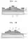
FIGS. 2A through 2H are cross-sectional views illustrating a method of manufacturing a TFT according to another embodiment of the present invention.
First, as illustrated in FIG. 2A, a gate electrode 14′ and a buffer layer 11′ are both formed on the substrate 10′ in a manner that is substantially the same as described above with reference to FIGS. 1A, 1B, and/or 1C.
After forming the gate electrode 14′, a gate insulating layer 13′ is formed on the gate electrode 14′ and the buffer layer 11′ as illustrated in FIG. 2B. In FIG. 2B, the gate insulating layer 13′ is illustrated to cover the gate electrode 14′; however, the method of manufacturing the TFT according to the current embodiment is not limited thereto.
After forming the gate insulating layer 13′, a patterned active layer 12′ is formed on the gate insulating layer 13′ as illustrated in FIG. 2C. The patterned active layer 12′ can be formed of an oxide semiconductor material that is substantially the same as described above with reference to the active layer 12.
After forming the patterned active layer 12′, a photoresist layer 30′ is formed on the patterned active layer 12′ to expose a source region 12b′ and a drain region 12c′ of the patterned active layer 12′. In more detail, as illustrated in FIG. 2D, the photoresist layer 30′ is formed on an entire surface of the substrate 10 (e.g., on the patterned active layer 12′ and the gate insulating layer 13′), and then the photoresist layer 30′ is patterned to expose the source region 12b′ and the drain region 12c′ of the patterned active layer 12′ as illustrated in FIG. 2E. The photoresist layer 30 can be patterned using a suitable photolithography method.
Then, as illustrated in FIG. 2F, by covering a channel region 12a′ of the patterned active layer 12′ with the patterned photoresist layer 30′ that acts as a mask, hydrogen ions are implanted into the exposed source region 12b′ and the drain region 12c′ of the patterned active layer 12′. In the present embodiment, an interlayer insulating layer is further formed before forming the photoresist layer 30′, and then the photoresist layer 30′ may be formed and patterned as described above. The hydrogen ions implanting is the same (or substantially the same) as described above and thus will not be described again.
Then, a conductive layer 17′ corresponding to an entire surface of the substrate 10′ is formed as illustrated in FIG. 2G. Due to the presence of the patterned photoresist layer 30′, the conductive layer 17′ is not formed as one unit so as to correspond to the entire surface of the substrate 10′; however, the conductive layer 17′ is formed on the patterned photoresist layer 30′ and on the exposed source region 12b′, the drain region 12c′ and the channel region 12a′ of the patterned active layer 12′. The conductive layer 17′ that is formed on the exposed source region 12b′ and the drain region 12c′ of the patterned active layer 12′, and the conductive layer 17′ formed on the patterned photoresist layer 30′ is separated as illustrated in FIG. 2G due to a step difference of the patterned photoresist layer 30′. The conductive layer 17′ may be formed of various suitable conductive materials, such as Al, Mo, W, Cr, Ni or compounds thereof and/or various suitable transparent conductive materials, such as ITO or IZO, as a single layer structure or a multi-layer structure.
Then, the patterned photoresist layer 30′ is removed using a lift-off method in order to pattern the conductive layer 17′ as illustrated in FIG. 2H. In other words, a source electrode 17a′ contacting the source region 12b′ of the patterned active layer 12′ and a drain electrode 17b′ contacting the drain region 12c′ of the patterned active layer 12′ are formed.
In view of foregoing and according to an embodiment of the present invention, a photoresist layer is used for implanting a source region and a drain region of an active layer (e.g., the active layer 12, 12′) with hydrogen ions as described above, and the photoresist layer is also consequently used for forming a source electrode and a drain electrode of a conductive layer. Thus, unlike a conventional TFT manufacturing method, which requires a doping process on semiconductor layers and a patterning process or mask process for forming a source electrode and a drain electrode, only one patterning process or one mask process, that is, a patterning of the photoresist layer, is needed according to the embodiment of the present invention. Thus, manufacturing costs are reduced and yield is increased.
In addition, according to a method of manufacturing a TFT according to an embodiment of the present invention as described above, the TFT is provided to have a source electrode, a drain electrode, and an active layer; and in which an ohmic contact can be formed between the source electrode and the active layer, or between the drain electrode and the active layer.
While the present invention has been described in connection with certain exemplary embodiments, it is to be understood that the invention is not limited to the disclosed embodiments, but, on the contrary, is intended to cover various modifications and equivalent arrangements included within the spirit and scope of the appended claims, and equivalents thereof.
Claims
What is claimed is:1. A thin film transistor (TFT) comprising:
a substrate;
an active layer disposed on the substrate and comprising a channel region, a source region, and a drain region, the active layer including a material selected from the group consisting of ZnO, InZnO, ZnSnO, and ZnInGaO;
a gate electrode insulated from the active layer;
a source electrode insulated from the gate electrode and electrically connected to the source region of the active layer; and
a drain electrode insulated from the gate electrode and electrically connected to the drain region of the active layer,
wherein the source region and the drain region of the active layer comprise hydrogen.
2. The TFT of claim 1, wherein a concentration of hydrogen of the source region and the drain region of the active layer ranges from about 1018/cm3 to about 1021/cm3.
3. The TFT of claim 1, wherein the substrate is a plastic substrate.
4. The TFT of claim 1, wherein the active layer is transparent to light.
5. The TFT of claim 1, further comprising a gate insulating layer disposed on the active layer to be between the gate electrode and the active layer, wherein the gate electrode is disposed on the gate insulating layer.
6. A thin film transistor (TFT) comprising:
a substrate;
a gate electrode disposed on the substrate;
an active layer including a material selected from the group consisting of ZnO, InZnO, ZnSnO, and ZnInGaO and insulated from the gate electrode, the active layer comprising a channel region, a source region, and a drain region;
a source electrode insulated from the gate electrode and electrically connected to the source region of the active layer; and
a drain electrode insulated from the gate electrode and electrically connected to the drain region of the active layer,
wherein the source region and the drain region of the active layer comprise hydrogen.
7. The TFT of claim 6, wherein a concentration of hydrogen of the source region and the drain region of the active layer ranges from about 1018/cm3 to about 1021/cm3.
8. The TFT of claim 6, wherein the substrate is a plastic substrate.
9. The TFT of claim 6, wherein the active layer is transparent to light.
10. The TFT of claim 6, further comprising a gate insulating layer disposed on the gate electrode to be between the gate electrode and the active layer, wherein the active layer is disposed on the gate insulating layer.
11. A method of manufacturing a thin film transistor (TFT), the method comprising:
forming an active layer on a substrate using a material selected from the group consisting of ZnO, InZnO, ZnSnO, and ZnInGaO, the active layer comprising a channel region, a source region, and a drain region;
forming a gate insulating layer to cover the active layer;
forming a gate electrode on the gate insulating layer;
implanting hydrogen ions on the gate insulating layer in order to inject hydrogen into the source region and the drain region of the active layer; and
forming a source electrode and a drain electrode to be electrically connected to the source region and the drain region of the active layer, respectively.
12. The method of claim 11, wherein during the implanting of the hydrogen ions, a hydrogen ion dose ranges from about 1 e16/cm2 to about 1 e18/cm2.
13. The method of claim 11, wherein during the implanting of the hydrogen ions, an injection energy of the hydrogen ions ranges from about 50 keV to about 150 keV.
14. The method of claim 11, further comprising:
heat treating the active layer after the implanting of the hydrogen ions.
15. The method of claim 14, wherein the heat treating of the active layer after the implanting of the hydrogen ions comprises heat treating the active layer at a temperature of about 200° C.
16. A method of manufacturing a thin film transistor (TFT), the method comprising:
forming a gate electrode on a substrate;
forming a gate insulating layer to cover the gate electrode;
forming an active layer comprising a channel region, a source region, and a drain region on the gate insulating layer using a material selected from the group consisting of ZnO, InZnO, ZnSnO, and ZnInGaO;
forming an interlayer insulating layer to cover the active layer;
implanting hydrogen ions into the interlayer insulating layer to inject hydrogen ions into the source region and the drain region of the active layer; and
forming a source electrode and a drain electrode to be electrically connected to the source region and the drain region of the active layer, respectively.
17. The method of claim 16, wherein during the implanting of the hydrogen ions, a hydrogen ion dose ranges from about 1 e16/cm2 to about 1 e18/cm2.
18. The method of claim 16, wherein during the implanting of the hydrogen ions, an injection energy of the hydrogen ions ranges from about 50 keV to about 150 keV.
19. The method of claim 16, further comprising:
heat treating the active layer after the implanting of the hydrogen ions.
20. The method of claim 19, wherein the heat treating of the active layer after the implanting of the hydrogen ions comprises heat treating the active layer at a temperature of about 200° C.
Images & Drawings included:


Sources:
- United States Patent and Trademark Office - verify current appl. status at the USPTO↗
Similar patent applications:
- » 20140145188
TRANSPARENT THIN FILM TRANSISTOR, AND METHOD OF MANUFACTURING THE SAME - » 20240234619
METHOD FOR MANUFACTURING TRANSPARENT THIN FILM TRANSISTOR-BASED PHOTOSENSITIVE DEVICE - » 20090127622
TRANSPARENT THIN-FILM TRANSISTOR AND MANUFACTURING METHOD OF THE TRANSISTOR - » 20230079198
Transparent conductive film, method of manufacturing same, thin film transistor, and device including same - » 20150187916
Method of manufacturing zinc oxide thin film, method of manufacturing thin film transistor, zinc oxide thin film, thin film transistor, and transparent oxide wiring - » 20150318502
TRANSPARENT ORGANIC THIN-FILM TRANSISTOR AND METHOD FOR MANUFACTURING SAME - » 20070057261
Transparent thin film transistor (TFT) and its method of manufacture - » 20070069209
Transparent thin film transistor (TFT) and its method of manufacture - » 20100243994
Transparent nonvolatile memory thin film transistor and method of manufacturing the same - » 20120225500
Transparent nonvolatile memory thin film transistor and method of manufacturing the same
Recent applications in this class:
- » 20240332321 2024-10-03
Display device and method of manufacturing the same - » 20240274625 2024-08-15
METHOD AND APPARATUS FOR MANUFACTURING DISPLAY DEVICE - » 20240038786 2024-02-01
ARRAY SUBSTRATE AND MANUFACTURING METHOD THEREOF - » 20240014227 2024-01-11
MANUFACTURING METHOD OF ARRAY SUBSTRATE, ARRAY SUBSTRATE, AND DISPLAY PANEL - » 20230352496 2023-11-02
Array substrate and display panel - » 20230154939 2023-05-18
Array substrate, preparation method thereof, and display panel - » 20230005966 2023-01-05
Display device and method of manufacturing the same - » 20220359575 2022-11-10
MANUFACTURING METHOD OF SEMICONDUCTOR DEVICE - » 20220310664 2022-09-29
DISPLAY SUBSTRATE AND METHOD FOR MANUFACTURING THE SAME - » 20220278134 2022-09-01
ARRAY SUBSTRATE AND METHOD OF MANUFACTURING THE SAME, AND DISPLAY APPARATUS
Recent applications for this Assignee:
- » 20250295018 2025-09-18
DISPLAY DEVICE AND OPTICAL DEVICE - » 20250295012 2025-09-18
DISPLAY DEVICE AND DISPLAY SYSTEM INCLUDING THE SAME - » 20250295004 2025-09-18
DISPLAY DEVICE - » 20250294994 2025-09-18
DISPLAY DEVICE - » 20250294975 2025-09-18
LIGHT-EMITTING DIODE, DISPLAY DEVICE INCLUDING THE SAME, AND ELECTRONIC DEVICE INCLUDING THE SAME - » 20250294969 2025-09-18
DISPLAY DEVICE, METHOD FOR MANUFACTURING THE DISPLAY DEVICE, AND HEAD MOUNTED DISPLAY INCLUDING THE DISPLAY DEVICE - » 20250294966 2025-09-18
DISPLAY DEVICE AND METHOD OF FABRICATING THE SAME - » 20250294960 2025-09-18
LIGHT-EMITTING ELEMENT AND DISPLAY DEVICE INCLUDING THE SAME - » 20250294941 2025-09-18
DISPLAY DEVICE AND MANUFACTURING METHOD THEREOF - » 20250291443 2025-09-18
ELECTRONIC DEVICE