Thin planar semiconductor device
US20080169550A1
2008-07-17
12/050,995
2008-03-19
✅ Patent granted
US 7,622,801 B2
2009-11-24
-
-
Andy Huynh
2028-03-19
Abstract:
A thin, planar semiconductor device having electrodes on both surfaces is disclosed. This semiconductor device is provided with an IC chip and a wiring layer having one side that is electrically connected to surface electrodes of the IC chip. On this surface of the wiring layer, conductive posts are provided on wiring of the wiring layer, and an insulating resin covers all portions not occupied by the IC chip and conductive posts. The end surfaces of the conductive posts are exposed from the insulating resin and are used as first planar electrodes. In addition, a resist layer is formed on the opposite surface of the wiring layer. Exposed portions are formed in the resist layer to expose desired wiring portions of the wiring layer. These exposed portions are used as second planar electrodes. Stacking semiconductor devices of this construction enables an improvement in the integration of semiconductor integrated circuits.
Assignee:
- NEC Corporation 20,055 🇯🇵 Tokyo, Japan
- NEC Electronics Corporation 1,733 🇯🇵 Kawasaki, Japan
Interested in similar patents?
Get notified when new applications in this technology area are published.
Classification:
H01L25/105 » CPC main
Assemblies consisting of a plurality of individual semiconductor or other solid state devices ; Multistep manufacturing processes thereof all the devices being of a type provided for in the same subgroup of groups - , e.g. assemblies of rectifier diodes the devices having separate containers the devices being of a type provided for in group
H01L25/0657 » CPC further
Assemblies consisting of a plurality of individual semiconductor or other solid state devices ; Multistep manufacturing processes thereof all the devices being of a type provided for in the same subgroup of groups - , e.g. assemblies of rectifier diodes the devices not having separate containers the devices being of a type provided for in group Stacked arrangements of devices
H01L21/568 » CPC further
Processes or apparatus adapted for the manufacture or treatment of semiconductor or solid state devices or of parts thereof; Manufacture or treatment of semiconductor devices or of parts thereof the devices having at least one potential-jump barrier or surface barrier, e.g. PN junction, depletion layer or carrier concentration layer; Assembly of semiconductor devices using processes or apparatus not provided for in a single one of the subgroups - , e.g. sealing of a cap to a base of a container; Encapsulations, e.g. encapsulation layers, coatings Temporary substrate used as encapsulation process aid
H01L2224/16 » CPC further
Indexing scheme for arrangements for connecting or disconnecting semiconductor or solid-state bodies and methods related thereto as covered by; Means for bonding being attached to, or being formed on, the surface to be connected, e.g. chip-to-package, die-attach, "first-level" interconnects; Manufacturing methods related thereto; Bump connectors; Manufacturing methods related thereto; Structure, shape, material or disposition of the bump connectors after the connecting process of an individual bump connector
H01L2224/81005 » CPC further
Indexing scheme for arrangements for connecting or disconnecting semiconductor or solid-state bodies and methods related thereto as covered by; Methods for connecting semiconductor or other solid state bodies using means for bonding being attached to, or being formed on, the surface to be connected using a bump connector involving a temporary auxiliary member not forming part of the bonding apparatus being a temporary or sacrificial substrate
H01L2225/06517 » CPC further
Details relating to assemblies covered by the group but not provided for in its subgroups; All the devices being of a type provided for in the same subgroup of groups - the devices not having separate containers the devices being of a type provided for in group; Stacked arrangements of devices Bump or bump-like direct electrical connections from device to substrate
H01L2225/0652 » CPC further
Details relating to assemblies covered by the group but not provided for in its subgroups; All the devices being of a type provided for in the same subgroup of groups - the devices not having separate containers the devices being of a type provided for in group; Stacked arrangements of devices Bump or bump-like direct electrical connections from substrate to substrate
H01L2225/06541 » CPC further
Details relating to assemblies covered by the group but not provided for in its subgroups; All the devices being of a type provided for in the same subgroup of groups - the devices not having separate containers the devices being of a type provided for in group; Stacked arrangements of devices Conductive via connections through the device, e.g. vertical interconnects, through silicon via [TSV]
H01L2225/06572 » CPC further
Details relating to assemblies covered by the group but not provided for in its subgroups; All the devices being of a type provided for in the same subgroup of groups - the devices not having separate containers the devices being of a type provided for in group; Stacked arrangements of devices Auxiliary carrier between devices, the carrier having an electrical connection structure
H01L2225/06582 » CPC further
Details relating to assemblies covered by the group but not provided for in its subgroups; All the devices being of a type provided for in the same subgroup of groups - the devices not having separate containers the devices being of a type provided for in group; Stacked arrangements of devices Housing for the assembly, e.g. chip scale package [CSP]
H01L2225/06586 » CPC further
Details relating to assemblies covered by the group but not provided for in its subgroups; All the devices being of a type provided for in the same subgroup of groups - the devices not having separate containers the devices being of a type provided for in group; Stacked arrangements of devices; Housing for the assembly, e.g. chip scale package [CSP] Housing with external bump or bump-like connectors
H01L2225/1035 » CPC further
Details relating to assemblies covered by the group but not provided for in its subgroups; All the devices being of a type provided for in the same subgroup of groups - the devices having separate containers the devices being of a type provided for in group the containers being in a stacked arrangement the lowermost container comprising a device support the device being entirely enclosed by the support, e.g. high-density interconnect [HDI]
H01L2225/1058 » CPC further
Details relating to assemblies covered by the group but not provided for in its subgroups; All the devices being of a type provided for in the same subgroup of groups - the devices having separate containers the devices being of a type provided for in group the containers being in a stacked arrangement; Details of electrical connections between containers Bump or bump-like electrical connections, e.g. balls, pillars, posts
H01L2924/15311 » CPC further
Indexing scheme for arrangements or methods for connecting or disconnecting semiconductor or solid-state bodies as covered by; Details of package parts other than the semiconductor or other solid state devices to be connected; Die mounting substrate; Connection portion the connection portion being formed only on the surface of the substrate opposite to the die mounting surface being a ball array, e.g. BGA
H01L2924/15331 » CPC further
Indexing scheme for arrangements or methods for connecting or disconnecting semiconductor or solid-state bodies as covered by; Details of package parts other than the semiconductor or other solid state devices to be connected; Die mounting substrate; Connection portion the connection portion being formed on the die mounting surface of the substrate the connection portion being formed both on the die mounting surface of the substrate and outside the die mounting surface of the substrate being a ball array, e.g. BGA
H01L2924/18161 » CPC further
Indexing scheme for arrangements or methods for connecting or disconnecting semiconductor or solid-state bodies as covered by; Details of package parts other than the semiconductor or other solid state devices to be connected; Encapsulation; Shape; Exposing the passive side of the semiconductor or solid-state body of a flip chip
H01L23/488 IPC
Details of semiconductor or other solid state devices; Arrangements for conducting electric current to or from the solid state body in operation, e.g. leads, terminal arrangements ; Selection of materials therefor consisting of soldered constructions
H01L23/22 IPC
Details of semiconductor or other solid state devices; Fillings or auxiliary members in containers or encapsulations , e.g. centering rings; Fillings characterised by the material, its physical or chemical properties, or its arrangement within the complete device liquid at the normal operating temperature of the device
Description
CROSS REFERENCE TO RELATED APPLICATION
This application is a divisional of U.S. patent application Ser. No. 11/345,780 filed Feb. 2, 2006, which is a divisional of U.S. patent application Ser. No. 10/100,974 filed Mar. 19, 2002, which claims priority from Japanese Patent Application Number 2001-086833 filed Mar. 26, 2001, the contents of which are hereby incorporated by reference.
BACKGROUND OF THE INVENTION
1. Field of the Invention
The present invention relates to a semiconductor device and to a method of fabricating the semiconductor device, and in particular, to the construction of a semiconductor device that can be three-dimensionally stacked and to a method of fabricating the semiconductor device.
2. Description of the Related Art
With the rapid development of Internet technology, prior-art constructions such as mainframes and terminals that are connected to mainframes have been replaced by systems made up by servers that are distributed throughout the world and the high-speed communication lines that connect them.
This information communication network is now rapidly coming into popular use in households and by individuals through inexpensive and highly functional personal computers or mobile telephones that can be connected to the Internet, and as a result, the next-generation Internet protocol (IPv6) will allow connection of all types of electrical household appliances to the Internet. It is desirable that the LSI that is incorporated in these mobile telephones and information electrical appliances be capable, by itself, of various types of processing ranging from information processing and information saving to input/output control. SoC (System on Chip), in which various function blocks are formed on a single LSI chip to realize a high-level multifunctional information processing system, is now receiving increased attention. In actuality, however, the simultaneous formation of various function blocks requiring different forming processes on a silicon wafer is problematic both in terms of design as well as fabrication. There is the additional problem that such LSI lacks flexibility when specifications are to be modified, such as when modifying the design or extending the functionality of each block.
In recent years, SiP (System in Package), in which a plurality of separate LSI are integrated into a package and systemized, has shown great promise as a countermeasure to this problem. In particular, in a package in which each individual LSI is provided as a separate module and then stacked three-dimensionally, each module is first tested to ensure against defects before being integrated. As a result, a higher yield of products that are free of defects and a higher degree of integration through three-dimensional packaging can be obtained than for an SoC in which a large number of functional elements are formed simultaneously or an SiP in which non-modular chips are stacked.
SUMMARY OF THE INVENTION
It is an object of the present invention to provide a novel semiconductor device and a method of fabricating the semiconductor device that can provide a solution to the above-described problems of the prior art, and in particular, that enables an improvement in integration through three-dimensional packaging.
In the semiconductor device of the first aspect of the present invention, surface electrodes of an IC chip are electrically connected to one surface of a planar wiring layer that is constituted by electrical wiring. Further, conductive posts are provided on the wiring of the wiring layer on one surface of the wiring layer, and an insulating resin covers areas in which the IC chip and conductive posts are not provided. The end surfaces of the conductive posts are exposed from the insulating resin.
A resist layer is formed on the opposite surface of the wiring layer. Exposed portions in which desired wiring portions of the wiring layer are exposed are formed in this resist layer.
According to the first aspect of the present invention, the end surfaces of the conductive posts on one surface of the wiring layer can be used as first planar electrodes, and the exposed portions of the wiring on the other surface of the wiring layer can be used as second planar electrodes.
In the first aspect of the semiconductor device, first electrode terminals may be formed on the end surfaces of the conductive posts. Second electrode terminals may also be formed on the wiring in the exposed portions. Ball-shaped solder may be used for the first electrode terminals and for the second electrode terminals.
The method of fabricating the semiconductor device of the above-described first aspect involves the following steps of:
preparing a wiring substrate that is constituted by a base material and a wiring layer that is composed of wiring that is formed on this base material, and an IC chip having electrode terminals formed on its surface;
providing conductive posts on desired wiring of the wiring layer of the wiring substrate;
connecting the surface electrodes of the IC chip to desired wiring of the wiring layer of the wiring substrate;
covering the IC chip and the conductive posts that have been arranged on the surface of the wiring layer of the wiring substrate and conductive bumps with an insulating resin;
removing the base material from the wiring substrate to expose the wiring layer;
forming a resist layer on the exposed wiring layer with the exception of desired wiring portions; and
grinding away the insulating resin to expose the end surfaces of the conductive posts.
The present invention thus can provide a stackable semiconductor device that lacks package material, thereby enabling a thin construction and a greater degree of freedom in design. The present invention therefore enables the realization of a high-capacity memory module or a System-in-Package.
As a second aspect, the present invention provides an assembled unit in which a plurality of semiconductor devices of the above-described first aspect is stacked. This assembled unit can be produced by electrically connecting the exposed portions of the wiring layer of one semiconductor device to the end surfaces of the conductive posts of another semiconductor device among the stacked semiconductor devices.
Finally, as a third aspect, the present invention provides a semiconductor device in which a planar wiring layer that is composed of wiring that is electrically connected to the end surfaces of conductive posts is provided in the semiconductor device of the first aspect. In this aspect, first electrode terminals may be formed on the wiring of the planar wiring layer that is made up by wiring that is electrically connected to the end surfaces of the conductive posts, and second electrode terminals may be formed on wiring of the exposed portions.
The above and other objects, features, and advantages of the present invention will become apparent from the following description with reference to the accompanying drawings, which illustrate examples of the present invention.
BRIEF DESCRIPTION OF THE DRAWINGS
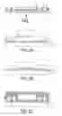
FIG. 1 is a sectional view of the semiconductor device according to the first embodiment of the present invention.
FIGS. 2A-2E show the fabrication steps of a semiconductor device according to the first embodiment example of the present invention.
FIG. 3 shows the semiconductor device according to the second embodiment of the present invention.
FIG. 4 shows the semiconductor device according to the third embodiment of the present invention.
DETAILED DESCRIPTION OF THE PREFERRED EMBODIMENTS
With the first working example of the semiconductor device of the present invention, referring to FIG. 1, IC chip 1 is arranged on one surface 3a of planar wiring layer 3. Wiring layer 3 is a layer composed of wiring such as signal lines, power supply lines, and ground lines. Electrodes 2 on the surface of IC chip 1 are electrically connected to desired wiring of wiring layer 3.
Wiring layer 3 is a structure in which a wiring substrate is formed by forming wiring on the surface of a planar base material, following which the base material is removed. IC chip 1 is a structure that has been made thin by grinding the rear surface.
On one surface 3a of wiring layer 3, protruding conductive posts 6 are electrically connected to the wiring that constitutes wiring layer 3. Although conductive posts 6 are formed as separate structures from the wiring of wiring layer 3 in this case, they may also be formed as a single unit with wiring layer 3. The height of conductive posts 6 is equal to the height of the rear surface of IC chip 1 that is arranged on the same surface 3a of wiring layer 3.
Still further, the vicinity of IC chip 1 and conductive posts 6 on this surface 3a of wiring layer 3 is covered with insulating resin 7. At least end surfaces 8 of conductive posts 6 are exposed from resin 7.
Solder resist layer 9 is formed on the opposite surface 3b of wiring layer 3. Exposed portions 10 for exposing desired wiring of the wiring that constitutes wiring layer 3 are formed in this solder resist layer 9. In other words, desired wiring portions on the opposite surface 3b of wiring layer 3 are not covered by solder resist layer 9.
According to the above-described construction, end surfaces 8 of conductive posts 6 on one surface 3a of wiring layer 3 can be used as first planar electrodes, and exposed portions 10 of wiring on the opposite surface 3b of wiring layer 3 can be used as the second planar electrodes.
In addition, ball-shaped solder may be affixed as electrode terminals to both or either of end surfaces 8 of conductive posts 6 and exposed portions 10 of the wiring of wiring layer 3 that are not covered by solder resist layer 9.
Explanation next regards the method of fabricating the above-described semiconductor device.
First, as shown in FIG. 2A, wiring substrate 4 is prepared that is constituted by base material 5 and wiring layer 3 in which electrical wiring is formed such as sign lines, power supply lines, and ground lines. Conductive posts 6 are then provided on the wiring that constitutes wiring layer 3. IC chip 1 in which bumps are used on surface electrodes 2 is also prepared.
Next, as shown in FIG. 2B, surface electrodes 2 of IC chip 1 are electrically connected (flip-chip attachment (FCA)) to the wiring of wiring layer 3 on wiring substrate 4.
Insulating resin 7 as shown in FIG. 2C next covers IC chip 1 and conductive posts 6 on wiring substrate 4, and resin 7 is hardened.
Base material 5 is next removed (Step a) from wiring substrate 4 to expose the opposite surface 3b that is on the opposite side of surface 3a of wiring layer 3, as shown in FIG. 2D. In addition, solder resist layer 9 is formed (Step b) on the opposite surface 3b of wiring layer 3 while leaving exposed portions 10 for exposing desired wiring of wiring layer 3. The film thickness of solder resist layer 9 is a maximum of 20 μm.
Resin 7, the rear surface of IC chip 1, and conductive posts 6 are next subjected to grinding to expose the end surfaces 8 of conductive posts 6, as shown in FIG. 2E (Step c).
The order of Step a, Step b, Step c is not limited to the order described hereinabove and may be determined as appropriate according to the manufacturing processes. The above-described procedure enables the formation of a thin planar semiconductor device that is shown in FIG. 1.
Explanation next regards the second embodiment example of the semiconductor device of the present invention.
The semiconductor device of the second embodiment that is shown in FIG. 3 is an assembled unit in which three of the semiconductor devices shown in FIG. 1 are stacked and electrically interconnected. Although there are three stacked layers in FIG. 3, the present invention is not limited to this number.
Referring now to FIG. 3, among vertically stacked semiconductor devices 13, exposed portions 10 of wiring layer 3 that are not covered by solder resist layer 9 of one semiconductor device 13 are connected by solder 11 to end surfaces 8 of conductive posts 6 that are provided on wiring layer 3 of another semiconductor device 13. In addition, ball-shaped solder 12 is affixed as electrode terminals to exposed portions 10 of wiring layer 3 that are not covered by solder resist layer 9 of lowermost semiconductor device 13.
Ball-shaped solder may also be affixed as electrode terminals to end surfaces 8 of conductive posts 6 of uppermost semiconductor device 13.
Stacking a plurality of layers of the semiconductor device shown in FIG. 1 to form an assembly as shown in FIG. 3 enables an improvement in the integration of semiconductor integrated circuits.
Explanation next regards the third embodiment of the semiconductor device of the present invention.
The semiconductor device of the third embodiment that is shown in FIG. 4 is a structure in which planar wiring layer 14 made up by electrical wiring is provided on surface 15 that is on the opposite side from solder resist layer 9 of the semiconductor device shown in FIG. 1, this planar wiring layer 14 being electrically connected to end surfaces 8 of conductive posts 6.
In this construction, ball-shaped solder may be affixed as first electrode terminals to exposed portions 10 of the wiring of wiring layer 3 as shown in FIG. 3, and moreover, ball-shaped solder may be affixed as second electrode terminals to desired wiring of wiring layer 14. Of course, a construction is also possible in which second electrode terminals are not affixed to wiring layer 14.
While preferred embodiments of the present invention have been described using specific terms, such description is for illustrative purposes only, and it is to be understood that changes and variations may be made without departing from the spirit or scope of the following claims.
Claims
What is claimed is:1. A semiconductor device comprising:
a wiring layer including a first wiring, said wiring layer having a first surface and a second surface opposing to said first surface;
an IC chip having an electrode on a front surface and mounted on said first surface to be electrically connected to said first wiring via said electrode;
a conductive post provided on said first surface to be electrically connected to said first wiring; and
insulating resin filling a space between said IC chip and said conductive post to form an upper surface opposite to said first surface and to expose an end surface of said conductive post;
wherein:
said wiring layer is formed by a continuous film so that an under surface of said insulating resin is covered completely with said wiring layer.
2. The semiconductor device as claimed in claim 1, wherein said end surface and said upper surface form a substantially flat and continuous surface.
3. The semiconductor device as claimed in claim 2, further comprising:
a second wiring on said second surface of said wiring layer.
4. The semiconductor device as claimed in claim 3, further comprising:
a third wiring formed on said upper surface to be electrically connected to said end surface.
5. The semiconductor device as claimed in claim 4, further comprising:
a solder ball formed between said end surface and said second wiring.
6. The semiconductor device as claimed in claim 3, further comprising:
a solder ball formed on said second wiring.
7. A semiconductor apparatus in which a plurality of semiconductor devices, according to claim 3, are stacked,
wherein:
an end surface of one of said plurality of semiconductor devices is electrically connected to a second wiring of another of said plurality of semiconductor devices.
8. The semiconductor device as claimed in claim 1, further comprising:
a third wiring formed on said upper surface to be electrically connected to said end surface.
9. The semiconductor device as claimed in claim 1, further comprising:
a solder ball formed on said end surface.
10. The semiconductor device as claimed in claim 1, wherein said wiring layer has a solder resist layer and is provided on an exposed portion on said second surface.
Images & Drawings included:


Sources:
- United States Patent and Trademark Office - verify current appl. status at the USPTO↗
Similar patent applications:
- » 10100974
Thin planar semiconductor device having electrodes on both surfaces and method of fabricating same - » 20060128060
Thin planar semiconductor device having electrodes on both surfaces and method of fabricating same - » 20080003828
Method for planarizing thin layer of semiconductor device - » 20150228792
Methods of forming a non-planar ultra-thin body semiconductor device and the resulting devices - » 20200373336
Semiconductor device including top gate planar type thin-film transistor and top gate planar self-aligned type thin-film transistor - » 20060163583
Semiconductor device comprising planarized light-shielding island films for thin-film transistors
Recent applications in this class:
- » 20250286027 2025-09-11
SYSTEM PACKAGING FOR CELLULAR MODEM AND TRANSCEIVER SYSTEM OF HETEROGENEOUS STACKING - » 20250286026 2025-09-11
SEMICONDUCTOR DEVICE WITH SPACER AND METHOD FOR FABRICATING THE SAME - » 20250286025 2025-09-11
SEMICONDUCTOR DEVICE WITH SPACER AND METHOD FOR FABRICATING THE SAME - » 20250286024 2025-09-11
SEMICONDUCTOR DEVICE WITH SPACER AND METHOD FOR FABRICATING THE SAME - » 20250259975 2025-08-14
SEMICONDUCTOR PACKAGE INCLUDING REDISTRIBUTION SUBSTRATE - » 20250233117 2025-07-17
METHOD OF FORMING SEMICONDUCTOR DEVICE USING HIGH STRESS CLEAVE PLANE - » 20250210601 2025-06-26
PIXEL ARRAY AND MANUFACTURING METHOD THEREFOR - » 20250210600 2025-06-26
SYSTEM-ON-CHIP GAP FILL METHOD AND STRUCTURE - » 20250201784 2025-06-19
SEMICONDUCTOR DEVICE HAVING PACKAGE ON PACKAGE STRUCTURE AND METHOD OF MANUFACTURING THE SEMICONDUCTOR DEVICE - » 20250183237 2025-06-05
PACKAGE STRUCTURE INCLUDING A BACKSIDE METAL FILM ON A SEMICONDUCTOR DIE AND A THERMALLY CONDUCTIVE UNDERFILL LAYER ON THE BACKSIDE METAL FILM AND METHODS OF FORMING THE SAME
Recent applications for this Assignee:
- » 20250295043 2025-09-18
SUPERCONDUCTING QUANTUM CIRCUIT - » 20250294700 2025-09-18
ELECTRONIC DEVICE RACK, ELECTRONIC DEVICE UNIT, AND METHOD OF INSTALLING ELECTRONIC DEVICE RACK - » 20250294570 2025-09-18
RADIO ACCESS NETWORK NODE, RADIO TERMINAL, AND METHODS AND NON-TRANSITORY COMPUTER-READABLE MEDIA THEREFOR - » 20250294518 2025-09-18
MONITORING DEVICE, TRACKING METHOD, AND NON-TRANSITORY COMPUTER-READABLE MEDIUM - » 20250294486 2025-09-18
METHOD, DEVICE AND COMPUTER READABLE MEDIUM FOR COMMUNICATIONS - » 20250294444 2025-09-18
CELL SELECTION BASED ON USER CAPABILITY - » 20250293871 2025-09-18
PRIVATE KEY RECOVERY DEVICE, PRIVATE KEY RECOVERY METHOD, AND STORAGE MEDIUM - » 20250293866 2025-09-18
QUANTUM KEY DISTRIBUTION SYSTEM, KEY MANAGEMENT APPARATUS, AND KEY MANAGEMENT METHOD - » 20250293833 2025-09-18
METHODS, DEVICES, AND COMPUTER READABLE MEDIUM FOR COMMUNICATION - » 20250293791 2025-09-18
COMMUNICATION CONTROL APPARATUS, COMMUNICATION APPARATUS, COMMUNICATION SYSTEM, STORAGE MEDIUM, AND COMMUNICATION CONTROL METHOD