Power switching circuit for liquid crystal display
US20080180870A1
2008-07-31
12/011,715
2008-01-28
✅ Patent granted
US 7,696,646 B2
2010-04-13
-
-
Stephen W Jackson | Adi Amrany
2028-10-15
Abstract:
An exemplary power switching circuit (20) includes a control signal input terminal (210); an output terminal (220); direct current (DC) power supply (230); a first transistor (250) including a control electrode connected to the control signal input terminal, a first current conducting electrode, and a grounded second current conducting electrode; a second transistor (260) including a control electrode connected to first current conducting electrode of the first transistor via a discharging resistor (264) and a diode (266) respectively and connected to the DC power supply via a discharging capacitor (265), a first current conducting electrode connected to the DC power supply, and a second current conducting electrode connected to the output terminal; and a third transistor (270) including a control electrode connected to first current conducting electrode of the first transistor, a first current conducting electrode connected to the output terminal, and a second grounded current conducting electrode.
Assignee:
- INNOLUX DISPLAY CORP. 205 🇹🇼 Miao-Li County, Taiwan
- Innocom Technology (Shenzhen) Co., Ltd. 196 🇨🇳 Shenzhen, Guangdong Province, China
Interested in similar patents?
Get notified when new applications in this technology area are published.
Classification:
H03K17/162 » CPC main
Electronic switching or gating, i.e. not by contact-making and –breaking; Modifications for eliminating interference voltages or currents in field-effect transistor switches without feedback from the output circuit to the control circuit
G09G3/3696 » CPC further
Control arrangements or circuits, of interest only in connection with visual indicators other than cathode-ray tubes for presentation of an assembly of a number of characters, e.g. a page, by composing the assembly by combination of individual elements arranged in a matrix no fixed position being assigned to or needed to be assigned to the individual characters or partial characters by control of light from an independent source using liquid crystals; Control of matrices with row and column drivers Generation of voltages supplied to electrode drivers
G09G2330/04 » CPC further
Aspects of power supply; Aspects of display protection and defect management Display protection
H03K17/6877 » CPC further
Electronic switching or gating, i.e. not by contact-making and –breaking characterised by the components used by the use, as active elements, of semiconductor devices the devices being field-effect transistors the control circuit comprising active elements different from those used in the output circuit
H03K19/0016 » CPC further
Logic circuits, i.e. having at least two inputs acting on one output ; Inverting circuits; Arrangements for reducing power consumption by using a control or a clock signal, e.g. in order to apply power supply
H03K19/017518 » CPC further
Logic circuits, i.e. having at least two inputs acting on one output ; Inverting circuits; Coupling arrangements; Interface arrangements; Interface arrangements using a combination of bipolar and field effect transistors [BIFET]
H01H89/00 IPC
Combinations of two or more different basic types of electric switches, relays, selectors and emergency protective devices, not covered by any single one of the other main groups of this subclass
H02H9/00 IPC
Emergency protective circuit arrangements for limiting excess current or voltage without disconnection
Description
FIELD OF THE INVENTION
The present invention relates to power switching circuits for liquid crystal displays (LCDs), and particularly to a power switching circuit employing one direct current (DC) power supply.
GENERAL BACKGROUND
An LCD has the advantages of portability, low power consumption, and low radiation, and has been widely used in various portable information products such as notebooks, personal digital assistants (PDAs), video cameras and the like. Furthermore, the LCD is considered by many to have the potential to completely replace CRT (cathode ray tube) monitors and televisions.
A typical LCD includes an LCD panel. The LCD panel includes a multiplicity of pixels, each having a capacitance. When a power supply provides an operation voltage to the LCD and then the power supply is turned off, the operation voltage does not immediately decrease. For example, when a power supply voltage of 5V is turned off, a decrease to a residual voltage 0.4 V takes about 20 seconds. If the power supply is turned on again quickly before the residual voltage in the power supply has decreased to a predetermined voltage, this causes an operational error in the LCD. To prevent such operational error, a power switching circuit is provided in the LCD to remove the residual voltage.
FIG. 3 is a circuit diagram of a typical power switching circuit 10 used in an LCD. The power switching circuit 10 includes a control signal input terminal 110 which is configured for receiving control signals, an output terminal 120 connected to the LCD, a twelve volt direct current (DC) power supply 130, a five volt DC power supply 140 functioning as a main power source of the LCD, a first negative-positive-negative (NPN) transistor 150, a second NPN transistor 170, an n-channel enhancement mode metal-oxide-semiconductor (NMOS) transistor 160, a first resistor 155, a second resistor 156, a third resistor 165, a fourth resistor 175, and a fifth resistor 176.
The first NPN transistor 150 includes a base electrode “b” connected to the control signal input terminal 110 via the first resistor 155, an emitter electrode “e” connected to the base electrode “b” via the second resistor 156 and further connected to ground, and a collector electrode “c” connected to the 12V DC power supply 130 via the third resistor 165.
The second NPN transistor 170 includes a base electrode “b” connected to the control signal input terminal 110 via the fourth resistor 175, an emitter electrode “e” connected to ground, and a collector electrode “c” connected to the output terminal 120 via the fifth resistor 176.
The NMOS transistor 160 includes a gate electrode “G” connected to the collector electrode “c” of the first NPN transistor 150, a source electrode “S” connected to the output terminal 120, and a drain electrode “D” connected to the 5V DC power supply 140.
In order to apply a 5V voltage from the 5V DC power supply 140 to the output terminal 120, a first control signal such as a low level 0V voltage is provided to the control signal input terminal 110 by an external circuit (not shown). Thus the first NPN transistor 150 and the second NPN transistor 170 are switched off. A 12V voltage from the 12V DC power supply 130 is applied to the gate electrode “G” of the NMOS transistor 160 via the third resistor 165. Thus the NMOS transistor 160 is switched on, and the 5V voltage from the 5V DC power supply 140 is applied to the output terminal 120 via the activated NMOS transistor 160.
In order to suspend the supply of the 5V voltage from the 5V DC power supply 140 to the output terminal 120, a second control signal such as a high level 5V voltage is provided to the control signal input terminal 110 by the external circuit. Thus the first NPN transistor 150 and the second NPN transistor 170 are switched on. The gate electrode “G” of the NMOS transistor 160 is connected to ground via the activated first NPN transistor 150, so that the NMOS transistor 160 is switched off. Thus, the 5V voltage from the 5V DC power supply 140 cannot be provided to the output terminal 120. Electric charges stored in the LCD which is connected to the output terminal 120 can be discharged quickly through the actived second NPN transistor 170.
Referring to FIG. 4, a current wave diagram of the power switching circuit 10 is shown. When the NMOS transistor 160 is switched on, and the supply of the 5V voltage is provided to the LCD via the activated NMOS transistor 160, a five amperes rush current is generated at the moment that the NMOS transistor 160 is switched on. The rush current may accelerate an aging process of electronic devices of the LCD. Thus a service life of the LCD is reduced.
It is desired to provide a new power switching circuit used in an LCD which can overcome the above-described deficiencies.
SUMMARY
In one preferred embodiment, a power switching circuit includes a control signal input terminal configured for receiving a control signal; an output terminal configured to be connected to a load circuit; a direct current (DC) power supply; a first transistor including a control electrode connected to the control signal input terminal, a first current conducting electrode, and a second current conducting electrode connected to ground; a second transistor including a control electrode connected to the first current conducting electrode of the first transistor via a discharging resistor and a diode respectively and connected to the DC power supply via a discharging capacitor, a first current conducting electrode connected to the DC power supply, and a second current conducting electrode connected to the output terminal; and a third transistor including a control electrode connected to first current conducting electrode of the first transistor, a first current conducting electrode connected to the output terminal, and a second current conducting electrode connected to ground.
Other novel features and advantages will become more apparent from the following detailed description when taken in conjunction with the accompanying drawings.
BRIEF DESCRIPTION OF THE DRAWINGS
FIG. 1 is a circuit diagram of a power switching circuit according to a preferred embodiment of the present invention, the power switching circuit being typically used in an LCD.
FIG. 2 is a current wave diagram of the power switching circuit of FIG. 1.
FIG. 3 is a circuit diagram of a conventional power switching circuit used in an LCD.
FIG. 4 is a current wave diagram of the power switching circuit of FIG. 3.
DETAILED DESCRIPTION OF PREFERRED EMBODIMENTS
Reference will now be made to the drawings to describe the present invention in detail.
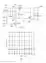
FIG. 1 is a current diagram of a power switching circuit 20 according to an exemplary embodiment of the present invention, the power switching circuit 20 being typically used in an LCD. The power switching circuit 20 includes a control signal input terminal 210 which is configured for receiving a control signal, an output terminal 220 configured for connecting to a load circuit (not shown) such as an LCD, a 3.3V DC power supply 240, a 5V DC power supply 230 functioning as a main power source of the load circuit, an NPN transistor 250, a p-channel enhancement mode metal-oxide-semiconductor (PMOS) transistor 260, a n-channel enhancement mode metal-oxide-semiconductor (NMOS) transistor 270, a first current limiting resistor 251, a second current limiting resistor 276, a first bias resistor 252, a second bias resistor 263, a third bias resistor 275, a discharge resistor 264, a charging capacitor 265, a diode 266, a first filter capacitor 221, a second filter capacitor 222, a third capacitor 231, and a fourth capacitor 232.
The control signal input terminal 210 is connected to the 3.3V DC power supply 240 via the first bias resistor 252.
A base electrode “b” of the NPN transistor 250 is connected to the control signal input terminal 210 via the first current limiting resistor 251. An emitter electrode “e” of the NPN transistor 250 is connected to ground. A collector electrode “c” of the NPN transistor 250 is connected to the five volt DC power supply 230 via the second bias resistor 263, and is further connected to a gate electrode “G” of the PMOS transistor 260 via the discharging resistor 264 and the diode 266 respectively. A positive terminal of the diode 266 is connected to the collector electrode “c” of the NPN transistor 250.
The charging capacitor 265 is connected between the gate electrode “G” and source electrode “S” of the PMOS transistor 260. The source electrode “S” of the PMOS transistor 260 is connected to the 5V DC power supply 230. A drain electrode “D” of the PMOS transistor 260 is connected to the output terminal 220.
A gate electrode “G” of the NMOS transistor 270 is connected to the collector electrode “c” of the NPN transistor 250 via the second current limiting resistor 276. A source electrode “S” of the NMOS transistor 270 is connected to ground. A drain electrode “D” of the NMOS transistor 270 is connected to the output terminal 220 via the third bias resistor 275.
The first filter capacitor 221 and the second filter capacitor 222 are connected between the output terminal 220 and ground, respectively. The third filter capacitor 231 and the fourth capacitor are connected between the 5V power supply 230 and ground, respectively.
In order to apply the 5V voltage from the DC power supply 230 to the output terminal 220, a first control signal such as a high level 5V voltage is provided to the control signal input terminal 210 by an external circuit (not shown). Thus the NPN transistor 250 is switched on and electric charges stored in the charging capacitor 265 are discharged to ground through the discharging resistor 264 and the activated NPN transistor 250 in series. Thus a voltage of the gate electrode “G” of the PMOS transistor 260 is slowly decreased to zero volts. A voltage difference between the gate electrode “G” and the source electrode “S” of the PMOS transistor 260 is slowly increased to approximately 5V, thus a channel of the PMOS transistor 260 is slowly open, and a current flows through the channel of the PMOS transistor is gradually increased. Accordingly, the 5V voltage from the DC power supply 230 is provided to the output terminal 220 via the PMOS transistor 260 without large current. Referring to FIG. 2, a current wave diagram of the power switching circuit 20 is shown. When the supply of the 5V voltage is gradually provided to the LCD via the PMOS transistor 260, a two amperes rush current is generated at the moment that the NMOS transistor 160 is switched on. At the same time, the gate electrode “G” of the NMOS transistor 270 is connected to ground via the second current limiting resistor 276 and the activated PMOS transistor 260. Thus the NMOS transistor 270 is switched off.
In order to suspend the supply of the 5V voltage from the DC power supply 230 to the output terminal 220, a second control signal such as a low level 0V voltage is provided to the control signal input terminal 210 by the external circuit. Thus the NPN transistor 250 is switched off. The 5V voltage of the DC power supply 230 is provided to the gate electrode “G” of the PMOS transistor 260 via the second bias resistor 263 and the diode 266 for quickly charging the charging capacitor 265. The voltage difference between the gate electrode “G” and the source electrode “S” of the PMOS transistor 260 is quickly decreased to 0V. Thus the channel of the PMOS transistor 260 is quickly pinched off and the PMOS transistor 260 is switched off. Therefore, the 5V voltage from the DC power supply 230 cannot be provided to the output terminal 220. At the same time, 5V voltage from the DC power supply 230 is provided to the gate electrode “G” of the NMOS transistor 270 for switching on the NMOS transistor 270. Electric charges stored in the load circuit which is connected to the output terminal 220 can be quickly discharged through the actived NMOS transistor 270.
Because the power switching circuit 20 includes the charging capacitor 265, the second bias resistor 263, the diode 266, and the charging resistor 264, the power switching circuit 20 can prevent a channel of the PMOS transistor 260 from being opened too quickly. Thus a rush current of a load circuit which is generated when a 5V voltage from the five volt DC power supply 230 is applied to an output terminal 220 can be reduced to only two amperes. Thus a service life of the load circuit such as LCD is increased.
In various alternative embodiments, each of the NPN transistors 250 can be replaced by an NMOS transistor, the PMOS transistor 260 can be replaced by a PNP transistor, and each of the NMOS transistors 270 can be replaced by an NPN transistor.
It is to be further understood that even though numerous characteristics and advantages of preferred and exemplary embodiments have been set out in the foregoing description, together with details of the structures and functions of the embodiments, the disclosure is illustrative only; and that changes may be made in detail, especially in matters of arrangement of parts within the principles of present invention to the full extent indicated by the broad general meaning of the terms in which the appended claims are expressed.
Claims
What is claimed is:1. A power switching circuit comprising:
a control signal input terminal configured for receiving a control signal;
an output terminal configured to be connected to a load circuit;
a direct current (DC) power supply;
a first transistor comprising a control electrode connected to the control signal input terminal, a first current conducting electrode, and a second current conducting electrode connected to ground;
a second transistor comprising a control electrode connected to the first current conducting electrode of the first transistor via a discharging resistor and a diode respectively and further connected to the DC power supply via a discharging capacitor, a first current conducting electrode connected to the DC power supply, and a second current conducting electrode connected to the output terminal; and
a third transistor comprising a control electrode connected to the first current conducting electrode of the first transistor, a first current conducting electrode connected to the output terminal, and a second current conducting electrode connected to ground.
2. The power switching circuit as claimed in claim 1, further comprising a first current limiting resistor connected between the control electrode of the first transistor and the control signal input terminal.
3. The power switching circuit as claimed in claim 1, further comprising a 3.3V DC power supply, and a first bias resistor connected between control signal input terminal and the 3.3V DC power supply.
4. The power switching circuit as claimed in claim 1, further comprising at least one filter capacitor connected between the output terminal and ground.
5. The power switching circuit as claimed in claim 1, further comprising at least one filter capacitor connected between DC power supply and ground.
6. The power switching circuit as claimed in claim 5, wherein the DC power supply is a 5V DC power supply.
7. The power switching circuit as claimed in claim 1, further comprising a second bias resistor connected between the first conducting electrode and the DC power supply.
8. The power switching circuit as claimed in claim 1, further comprising a third bias resistor connected between the first current conducting electrode and the output terminal.
9. The power switching circuit as claimed in claim 1, further comprising a second current limiting resistor connected between the control electrode and the first conducting electrode.
10. The power switching circuit as claimed in claim 1, wherein the control signal is a high level voltage or a low level voltage.
11. The power switching circuit as claimed in claim 1, wherein the first transistor is an n-channel enhancement mode metal-oxide-semiconductor (NMOS) transistor.
12. The power switching circuit as claimed in claim 1, wherein the first transistor is a negative-positive-negative (NPN) transistor.
13. The power switching circuit as claimed in claim 1, wherein the second transistor is a p-channel enhancement mode metal-oxide-semiconductor (PMOS) transistor.
14. The power switching circuit as claimed in claim 1, wherein the second transistor is a positive-negative-positive (PNP) transistor.
15. The power switching circuit as claimed in claim 1, wherein the third transistor is an n-channel enhancement mode metal-oxide-semiconductor (NMOS) transistor.
16. The power switching circuit as claimed in claim 1, wherein the third transistor is an negative-positive-negative (NPN) transistor.
17. The power switching circuit as claimed in claim 1, wherein the load circuit is comprised in a liquid crystal display.
Images & Drawings included:


Sources:
- United States Patent and Trademark Office - verify current appl. status at the USPTO↗
Similar patent applications:
- » 20070252637
Power switching circuit and liquid crystal display using same - » 20080037186
Power switching circuit and liquid crystal display using same - » 20180287486
Circuit and switching power supply and liquid crystal display driving circuit - » 20160379581
Switching power supply circuit, liquid crystal driving device, and liquid crystal display device - » 20160351146
Switching power supply circuit, liquid crystal driving device, and liquid crystal display device - » 20170108724
Power conversion circuit for switching viewing angle and liquid crystal display - » 20170213510
Switching power supply circuit, load driving device, and liquid crystal display device - » 20080180977
Power supply control circuit having controllable switch and liquid crystal display using the same - » 20200341310
Thin film transistor liquid crystal display (TFT-LCD) and the driving circuit and switching power supply thereof - » 20090273953
Inverter for a liquid crystal display device with soft start circuit to overcome power loss in transistor switching
Recent applications in this class:
- » 20250293683 2025-09-18
FILTER WITH LOW LEAKAGE POWER-DOWN SWITCHES - » 20250274117 2025-08-28
SEMICONDUCTOR DEVICE AND METHOD OF CONTROLLING SEMICONDUCTOR DEVICE - » 20250266822 2025-08-21
NON-OVERLAPPING GENERATION TECHNIQUE FOR BOOTSTRAP SWITCHES - » 20250247091 2025-07-31
POWER SWITCH CIRCUIT - » 20250240013 2025-07-24
MOTOR DRIVER IMPROVING RESONANCE NOISE CAUSED BY MOTOR - » 20250219634 2025-07-03
SIGNAL TRANSMITTING APPARATUS - » 20250202474 2025-06-19
SWITCHING SLEW RATE CONTROL OF CASCODE SWITCH DEVICE AND GATE DRIVER THEREOF - » 20250202473 2025-06-19
SOLID STATE SWITCH DEVICE - » 20250192767 2025-06-12
LOW LEAKAGE CURRENT FEEDTHROUGH SWITCH - » 20250132759 2025-04-24
Method And Apparatus For Use In Digitally Tuning A Capacitor In An Integrated Circuit Device
Recent applications for this Assignee:
- » 20180335674 2018-11-22
Liquid crystal display device - » 20150062470 2015-03-05
Three-dimensional image display apparatus - » 20140285739 2014-09-25
Capacitance touch panel module and fabrication method thereof - » 20140217399 2014-08-07
Active matrix image sensing panel and apparatus - » 20140093252 2014-04-03
Shift register circuit and display device using the same - » 20140063378 2014-03-06
Three-dimensional image display apparatus - » 20130307791 2013-11-21
Method of minimizing charges accumulated at common electrode of display panel - » 20130249875 2013-09-26
OLED-based display device including a pixel circuit, and driving methods thereof - » 20130207169 2013-08-15
Active matrix image sensing panel and apparatus - » 20130147856 2013-06-13
Display driving method with variable scan driving signal, driving module with variable scan driving signal, and display apparatus with variable scan driving signal