Burn-in socket having loading plate with uneven seating surface
US20080299792A1
2008-12-04
12/156,023
2008-05-28
✅ Patent granted
US 7,556,518 B2
2009-07-07
-
-
Javaid Nasri
2028-05-28
Abstract:
A burn-in socket for receiving an IC package includes a base defining an opening for loading the IC package. A loading plate is mounted within the base. The loading plate has a seating surface with a number of holes defined therein. A contact socket is located under the loading plate. A number of contacts are received in the contact socket. Each contact has one end extending into the hole in the seating surface of the loading plate for contact with a solder ball of the IC package. The seating surface comprises at least one lower plane and at least one upper plane. At least the upper plane is formed with the holes.
Assignee:
- Hon Hai Precision Ind. Co., Ltd. 1,929 🇹🇼 Taipei Hsien, Taiwan
Interested in similar patents?
Get notified when new applications in this technology area are published.
Classification:
G01R31/2863 » CPC main
Arrangements for testing electric properties; Arrangements for locating electric faults; Arrangements for electrical testing characterised by what is being tested not provided for elsewhere; Testing of electronic circuits, e.g. by signal tracer; Testing of integrated circuits [IC]; Environmental, reliability or burn-in testing; External aspects, e.g. related to chambers, contacting devices or handlers Contacting devices, e.g. sockets, burn-in boards or mounting fixtures
G01R1/0483 » CPC further
Details of instruments or arrangements of the types included in groups - and; General constructional details; Housings; Supporting members; Arrangements of terminals; Test fixtures or contact fields; Connectors or connecting adaptors; Test clips; Test sockets; Sockets for IC's or transistors Sockets for un-leaded IC's having matrix type contact fields, e.g. BGA or PGA devices; Sockets for unpackaged, naked chips
H01R12/00 IPC
Structural associations of a plurality of mutually-insulated electrical connecting elements, specially adapted for printed circuits, e.g. printed circuit boards [PCBs], flat or ribbon cables, or like generally planar structures, e.g. terminal strips, terminal blocks; Coupling devices specially adapted for printed circuits, flat or ribbon cables, or like generally planar structures; Terminals specially adapted for contact with, or insertion into, printed circuits, flat or ribbon cables, or like generally planar structures
H01R13/62 IPC
Details of coupling devices of the kinds covered by groups or - Means for facilitating engagement or disengagement of coupling parts or for holding them in engagement
H01R13/15 IPC
Details of coupling devices of the kinds covered by groups or -; Contact members Pins, blades or sockets having separate spring member for producing or increasing contact pressure
Description
BACKGROUND OF THE INVENTION
1. Field of the Invention
This invention relates generally to a burn-in socket for removably loading an IC package having a plurality of solder balls in order to make an electrical connection with contacts of the socket, and more particularly, to a burn-in socket having a loading plate adapt for a type of IC package which has protrusions at the bottom thereof, and else adapt for at least two type of IC packages of different configurations.
2. Description of the Related Art
IC packages are usually subjected to pass a so-called burn-in test, in which the IC packages are placed in an oven and operated for a time at an elevated temperature, and under a voltage source that is greater than the rated value. Those IC packages that continue to perform satisfactorily are then approved for shipment.
An IC package generally defines a top surface and a bottom surface. A plurality of conducting leads, for example solder balls, are attached to the bottom surface for electrical contact with the terminals of a burn-in socket. One type of the IC package for example is called DDR package (DDR hereinafter), which is widely used in memory storage. Parts of the types of the conventional DDRs are equipped with some protrusions or ribs at the bottom surface and between two sets of solder balls, according to the IC designers.
U.S. Pat. No. 7,210,951 issued to Sinclair on May 1, 2007 discloses a top loaded burn-in socket for forming a plurality of electrical connections between a ball gird array (BGA) package having a plurality of conductive ball leads and an electrical component. The socket assembly includes a plurality of resilient electrical contacts; a cam being configured to position the contacts from a first position to a second position; a device guide plate including a plurality of openings for receiving the ball leads; and an actuating mechanism configured to interact with the cam to position the contacts, wherein an upper portion of the contacts engages the ball leads between the upper portion and an inclined surface of the device guide plate openings. Each ball is thus held in a manner that does not require the use of a hold down mechanism for effecting electrical continuity between the BGA package and the contacts of the subject burn-in socket.
However, it is noted that the one problem is likely to be caused when such an IC package like DDR is loaded in the above burn-in socket that the protrusions at the bottom surface of DDR interfere with the planar up surface 90 of the burn-in socket, and it will prevent the insertion of solder balls of the IC package into the plurality of holes formed in the planar up surface 90. Another problem is also exists in this conventional burn-in socket, that only one type of IC package could be loaded and tested. The guide plate has to be redesigned when a new IC package of different configuration is to be loaded, and therefore the cost is raised.
BRIEF SUMMARY OF THE INVENTION
Accordingly, it is an object of the present invention to provide a burn-in socket adapted for an IC package with protrusions at the bottom thereof.
It is another object of the present invention to provide a burn-in socket adapted for at least two types of IC packages of different configurations.
According to one aspect of the present invention, a burn-in socket for receiving an IC package is provided. The burn-in socket includes a base defining an opening for loading the IC package. A loading plate is mounted within the base. The loading plate has a seating surface with a plurality of holes defined therein. A contact socket is located under the loading plate. A plurality of contacts are received in the contact socket. Each contact has one end extending into the hole in the seating surface of the loading plate for contact with a solder ball of the IC package. The seating surface comprises at least one lower plane and at least one upper plane. At least the upper plane is formed with the holes.
According to another aspect of the present invention, a burn-in socket for receiving an IC package is provided. The burn-in socket includes a base defining an opening for loading the IC package. A loading plate is mounted within the base. The loading plate has a seating surface with a plurality of holes defined therein. A contact socket is located under the loading plate. A plurality of contacts are received in the contact socket. Each contact has one end extending into the hole in the seating surface of the loading plate for contact with a solder ball of the IC package. The seating surface has at least one recess for accommodation of at least one protrusion which is formed at a bottom surface of the IC package.
Other objects, advantages and novel features of the present invention will become more apparent from the following detailed description of the present embodiment when taken in conjunction with the accompanying drawings.
BRIEF DESCRIPTION OF THE DRAWINGS
FIG. 1 is an assembled, perspective view of a burn-in socket according to an embodiment of the present invention;
FIG. 2 is a sectional exploded, perspective view of the burn-in socket;
FIG. 3 is an opposite view of the FIG. 2;
FIG. 4 is an assembled, perspective view of latching mechanisms according to the embodiment of the present invention;
FIG. 5 is a sectional assembled, perspective view of the burn-in socket in a closed state, according to the embodiment of the present invention;
FIG. 6 is a sectional assembled, perspective view of the burn-in socket in a open state, according to the embodiment of the present invention;
FIG. 7 is another angled view of FIG. 6;
FIG. 8 is an exploded, perspective view of contact socket according to the embodiment of the present invention;
FIG. 9 is an assembled, perspective view of FIG. 8;
FIG. 10 is a perspective view of a loading plate according to the embodiment of the present invention;
FIG. 11A is a bottom view of an IC package to be tested in the burn-in socket of present invention; and
FIG. 11B is a side view of the IC package in the FIG. 11A.
DETAILED DESCRIPTION OF THE INVENTION
Following is the description of the best embodiment of the burn-in socket 1 of present invention. In this best embodiment, the burn-in socket 1 is designed to be capable of receiving two IC packages synchronously. The burn-in socket 1 in use is generally mounted on a printed circuit board (not shown).
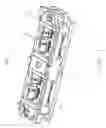
Referring to FIG. 1 to FIG. 3 and FIG. 5 to FIG. 7, the burn-in socket 100 includes a base 1, a pair of loading plates 5 mounted with the base 1, and a contact socket 7 located under the loading plates 5.
The base 1 has a longwise configuration and defines a pair of openings 10 for loading the IC packages. A driver 2 with a similar longwise configuration as the base 1 is movably mounted above the base 1 to drive two pairs of latching mechanisms 3. The driver 2 also defines a pair of openings 20, respectively corresponding to the openings 10 of base 1 to load the IC packages. The driver 2 is driven by a downward operation force and is urged to move downwardly to drive the latching mechanism 3. Referring to FIG. 4, the latching mechanism 3 constitutes of a latch 30 and a torsion spring 31 engaging with the latch 30. The performance of the latch mechanisms 3 being driven by the driver 2, as a conventional technology, will not be described here again. When the driver 2 is fully pressed to a lowest position, the burn-in socket 100 is in an open state, with the latches 30 turned upwardly ready for loading the IC package. The driver 2 gets back to its original position by elastic force generated by springs 21 when the operation force is released, and the burn-in socket turns to be a closed state, with the latches 30 closed for latching the IC package.
Please now referring to FIG. 2-3 and FIG. 10, the pair of loading plates 5 are mounted at the bottom of the base 1. The loading plate 5 and the base 1 are also positioned with each other by means of lifting elements 4, each of which is equipped by a rod 40 and a spring 41. Another function of the lifting element 4 is to support the loading plate 5 and urge it to stick to the IC package. The loading plate 5 is made of dielectric material and has an approximate rectangular configuration. The loading plate 5 has a seating surface 50 at the middle portion for supporting the IC package. The seating surface 50 is formed with a un-flat configuration, which constitutes of a central lower plane 51, a pair of upper planes 52 respectively at two lateral sides of the central lower plane 51 and abut against the central lower plane 51, respectively, and a pair of side lower planes 53 located at the side-most position of the seating surface 50 and respectively abuts against one upper plane 52. In other words, upper planes 52 and lower planes 53 are alternately arranged. Each lower plane 51, 53 defines a recess (not labeled), respectively. All the central lower planes 51, the upper planes 52 and the side lower planes 53 are respectively formed with a set of holes 510, 520, 530. Further a rectangular opening 511 is formed in the middle of the central lower plane 51 and divides the holes 510 into two groups. A sensor (not shown) could be used to inspect the loading of the IC package through the opening 511.
Please now referring to FIG. 8 and FIG. 9, the contact socket 7 in use is normally positioned on a circuit board (not shown), and then the assembly of base 1, cover 2 and loading plates 5 is laid on the contact socket 7. The contact socket 7 includes a frame 70 formed with a similar longwise configuration as the base 1 and the cover 2, a pair of top plate 71, and a pair of bottom plate 72. The top plate 71 is stacked on corresponding bottom plate 71, and then are together mounted within the frame 70. The top plate 71 and bottom plate 72 are formed with a plurality of passageways 710, 720, respectively. A plurality of contacts 6 are vertically received in the passageways 710, 720, each with one end extending upwardly out of the top plate 71 and extending into the hole 510, 520, 530 to contact with the solder ball of the IC package, and the other end contacting with an electric pad (not shown) on the circuit board.
Referring to FIG. 11A and FIG. 11B, it is a special IC package 8 that proper to be tested in the burn-in socket 100 of present invention. The IC package 8 comprises a plate-shaped body 80 and two groups of solder balls 81 attached at the bottom surface of the body 80. A longitude protrusion 82 is formed between the two groups of solder balls 81, and further a plurality of small protrusions 83 are formed at two sides of the bottom surface of the body 80. The lowest point of each protrusion 82, 83 in a vertical direction is higher than the lowest point of the solder ball 81. When this IC package 8 is loaded to the burn-in socket 100 to seat on the loading surface 50 of the loading plate 5, the longitude protrusion 82 is accommodated in the recess defined by the central lower plane 51, and the small protrusions 83 at side positions are accommodated in the recesses defined by the side lower planes 53. Therefore, the solder balls 81 are able to be inserted to the holes 520 in the upper planes 52 without any block, to achieve electrical connection with the contacts 6 which respectively has one end extending into the hole 520.
It can be seen that only the contacts 6 which extend into the holes 520 of upper planes 52 are used to be connected with the IC package 8. Further, another type of IC package which has different configuration as the above IC package 8 is also proper to be test in the IC package 100 of the present invention. For example, different number of the solder balls or different arrangement of the solder balls is adopted, and in these cases, the contacts 6 which extend to the holes 510, 530 of the lower planes 51, 53 may be used.
Claims
What is claimed is:1. A burn-in socket for receiving an IC package comprising:
a base defining an opening for loading the IC package therein;
a loading plate mounted within the base, the loading plate having a seating surface with a plurality of holes defined therein;
a contact socket located under the loading plate; and
a plurality of contacts received in the contact socket, each contact having one end extending into the hole in the seating surface of the loading plate for contact with a solder ball of the IC package;
wherein the seating surface comprises at least one lower plane and at least one upper plane, and at least said upper plane is formed with said holes.
2. The burn-in socket according to claim 1, wherein the loading plate has two upper planes and said at least one lower plane is between the two upper planes.
3. The burn-in socket according to claim 2, wherein the loading plate has a central lower plane and two side lower planes, and all the lower planes and upper planes are alternately arranged.
4. The burn-in socket according to claim 3, wherein the central lower plane has an opening formed therein for inspecting the loading of the IC package.
5. The burn-in socket according to claim 1, further comprising a cover which is provided to drive at least one latching mechanism, the cover moving in a vertical direction relative to the base.
6. The burn-in socket according to claim 1, wherein the contact socket comprises a frame and at least one plate mounted within the frame, the plate being formed with a plurality of passageways for receiving the contacts.
7. The burn-in socket according to claim 1, at least one lifting element is provided to support the loading plate and urge it to stick to the IC package.
8. A burn-in socket for receiving an IC package comprising:
a base defining an opening for loading the IC package;
a loading plate mounted within the base, the loading plate having a seating surface with a plurality of holes defined therein;
a contact socket located under the loading plate; and
a plurality of contacts received in the contact socket, each contact having one end extending into the hole in the seating surface of the loading plate for contact with a solder ball of the IC package;
wherein the seating surface has at least one recess for accommodation of at least one protrusion which is formed at a bottom surface of the IC package.
9. The burn-in socket according to claim 8, wherein said at least one recess is defined by a lower plane.
10. The burn-in socket according to claim 9, wherein the loading plate has a central lower plane and a pair of side lower planes, each of which defines a recess.
11. The burn-in socket according to claim 10, wherein the loading plate has a pair of upper planes formed beside the central lower plane respectively.
12. The burn-in socket according to claim 11, wherein all the lower planes and upper planes are alternately arranged.
13. The burn-in socket according to claim 12, wherein the central lower plane has an opening formed therein for inspecting the loading of the IC package.
14. The burn-in socket according to claim 8, further comprising a cover which is provided to drive at least one latching mechanism, the cover moving in a vertical direction relative to the base.
15. The burn-in socket according to claim 8, wherein the contact socket comprises a frame and at least one plate mounted within the frame, the plate being formed with a plurality of passageways for receiving the contacts.
16. The burn-in socket according to claim 8, at least one lifting element is provided to support the loading plate and urge it to stick to the IC package.
17. A burn-in socket for receiving an IC package comprising:
a base defining an opening for loading the IC package therein;
a cover up and down moveable relative to the base between upper and lower positions;
a first spring urging the cover away from the base;
a loading plate mounted within the base, the loading plate having a seating surface with a plurality of holes defined therein;
a contact socket located under the loading plate;
a plurality of contacts received in the contact socket, each contact having one end extending into the hole in the seating surface of the loading plate for contact with a solder ball of the IC package; and
a latch mechanism pivotally associated with the base, and actuated to rotate to a horizontally locking position via the cover; wherein
the latch mechanism is equipped with a second spring to urge the latch mechanism is fully moved away from the locking position to a fully open position once the cover is moved relative to the base to said lower position and the latch mechanism is no longer urged by the cover.
Images & Drawings included:


Sources:
- United States Patent and Trademark Office - verify current appl. status at the USPTO↗
Recent applications in this class:
- » 20250283936 2025-09-11
SOCKET RANKING METHOD FOR SEMICONDUCTOR TEST APPARATUS AND SEMICONDUCTOR TEST METHOD USING THE SOCKET RANKING METHOD - » 20250277845 2025-09-04
TEST BOARD FOR BURN-IN TEST - » 20250216442 2025-07-03
SOCKET ASSEMBLY AND ELECTRONIC COMPONENT TEST APPARATUS - » 20250155492 2025-05-15
MULTI-WAFER INSPECTION SYSTEM - » 20250138085 2025-05-01
LIQUID COOLED TEST SYSTEM FOR TESTING SEMICONDUCTOR INTEGRATED CIRCUIT CHIPS - » 20250130274 2025-04-24
SEMICONDUCTOR BURN-IN BOARD - » 20250093405 2025-03-20
SHELL FOR WAFER LEVEL BURN-IN (WLBI) CHIP TEST, METHOD FOR LOADING SAID SHELL AND MACHINE FOR BURN-IN TEST COMPRISING SAID SHELL - » 20250035699 2025-01-30
CONTACT PROBE, PROBE HOLDER AND PROBE UNIT - » 20250012853 2025-01-09
METHODS AND APPARATUS TO DISENGAGE A TEST HEAD FROM AN INTEGRATED CIRCUIT (IC) DEVICE - » 20240264223 2024-08-08
INTEGRATED ACTUATOR TEST SYSTEM AND METHOD FOR OPERATING THE SAME
Recent applications for this Assignee:
- » 20110045702 2011-02-24
Electrical cable connector assembly with improved wire organizer - » 20110021088 2011-01-27
Electrical connector with improved contact footprints - » 20110021082 2011-01-27
High density backplane connector having improved terminal arrangement - » 20110008982 2011-01-13
N-in-1 card connector - » 20110005825 2011-01-13
Cable assembly with EMI protection - » 20110003508 2011-01-06
Electrical connector rotatably mounted to a portable device - » 20100330822 2010-12-30
Electrical connector having contact with upper terminal and lower terminal - » 20100317218 2010-12-16
Electrical connector assembly with latching mechanism - » 20100297861 2010-11-25
Socket connector having improved actuating mechanism for driving moving plate - » 20100291799 2010-11-18
Shielded connector with enlarged base supporting cantilevered brackets extending from the shielded connector