Materials for N-doping the electron-transporting layers in organic electronic components
US20090114906A1
2009-05-07
12/065,862
2006-08-23
✅ Patent granted
US 8,481,785 B2
2013-07-09
WO; PCT/EP2006/065580; 20060823
WO; WO2007/028712; 20070315
Gerard Higgins | J. L. Yang
Fish & Richardson P.C.
2027-04-09
Abstract:
New materials for the n-doping of the elctron-transporting layer in organic electronic components, their utilization, and organic electronic components
The invention pertains to new materials based on sterically inhibited donor arylboranes for the improvement of electron injection and electron transport in organic electronic components like organic light-emitting diodes (OLED's), organic field effect transistors (OFET's), and on organic photovoltaics based components, in particular, organic solar cells.
Assignee:
- OSRAM OPTO SEMICONDUCTORS GMBH 1,822 🇩🇪 Regensburg, Germany
- Osram Opto Semiconductors GmbH 1 🇩🇪 93055 Regensburg, Germany
Applicant:
Interested in similar patents?
Get notified when new applications in this technology area are published.
Classification:
H01L51/002 » CPC main
Solid state devices using organic materials as the active part, or using a combination of organic materials with other materials as the active part; Processes or apparatus specially adapted for the manufacture or treatment of such devices, or of parts thereof; Processes specially adapted for the manufacture or treatment of devices or of parts thereof Making n- or p-doped regions
C07F5/027 » CPC further
Compounds containing elements of Groups 3 or 13 of the Periodic System; Boron compounds Organoboranes and organoborohydrides
H01L51/006 » CPC further
Solid state devices using organic materials as the active part, or using a combination of organic materials with other materials as the active part; Processes or apparatus specially adapted for the manufacture or treatment of such devices, or of parts thereof; Selection of organic semiconducting materials, e.g. organic light sensitive or organic light emitting materials; Macromolecular systems with low molecular weight, e.g. cyanine dyes, coumarine dyes, tetrathiafulvalene; Amine compounds having at least two aryl rest on at least one amine-nitrogen atom, e.g. triphenylamine comprising polycyclic condensed aromatic hydrocarbons as substituents on the nitrogen atom
H01L51/008 » CPC further
Solid state devices using organic materials as the active part, or using a combination of organic materials with other materials as the active part; Processes or apparatus specially adapted for the manufacture or treatment of such devices, or of parts thereof; Selection of organic semiconducting materials, e.g. organic light sensitive or organic light emitting materials; Coordination compounds, e.g. porphyrin; Metal complexes comprising a IIIB-metal (B, Al, Ga, In or TI), e.g. Tris (8-hydroxyquinoline) gallium (Gaq3) comprising boron
H01L51/5076 » CPC further
Solid state devices using organic materials as the active part, or using a combination of organic materials with other materials as the active part; Processes or apparatus specially adapted for the manufacture or treatment of such devices, or of parts thereof specially adapted for light emission, e.g. organic light emitting diodes [OLED] or polymer light emitting devices [PLED]; Carrier transporting layer; Electron transporting layer comprising a dopant
H01L51/0545 » CPC further
Solid state devices using organic materials as the active part, or using a combination of organic materials with other materials as the active part; Processes or apparatus specially adapted for the manufacture or treatment of such devices, or of parts thereof specially adapted for rectifying, amplifying, oscillating or switching, or capacitors or resistors with at least one potential- jump barrier or surface barrier multistep processes for their manufacture the devices being controllable only by the electric current supplied or the electric potential applied, to an electrode which does not carry the current to be rectified, amplified or swiched, e.g. three-terminal devices; Field-effect devices, e.g. TFTs insulated gate field effect transistors Lateral single gate single channel transistors with inverted structure, i.e. the organic semiconductor layer is formed after the gate electrode
Y02E10/549 » CPC further
Energy generation through renewable energy sources; Photovoltaic [PV] energy Organic PV cells
Y02E10/549 » CPC further
Energy generation through renewable energy sources; Photovoltaic [PV] energy Organic PV cells
H01L51/00 IPC
Solid state devices using organic materials as the active part, or using a combination of organic materials with other materials as the active part; Processes or apparatus specially adapted for the manufacture or treatment of such devices, or of parts thereof
C07F5/02 IPC
Compounds containing elements of Groups 3 or 13 of the Periodic System Boron compounds
C07D417/02 IPC
Heterocyclic compounds containing two or more hetero rings, at least one ring having nitrogen and sulfur atoms as the only ring hetero atoms, not provided for by group containing two hetero rings
Description
The invention pertains to new materials for the improvement of the electron injection and the electron transport in organic components like organic light-emitting diodes (OLED's), organic field effect transistors (OFET's), and organic solar cells.
In recent years materials, in particular for organic light-emitting diodes, have become known, which improve electron injection and electron transport in OLED's. (Lit.: S. Yamaguchi, S. Akiyama, K. Tamao, J. Am. Chem. Soc. 2000, 122 6335-6336).
This also results in a lower operating voltage without affecting the efficiency of the OLED. These materials are strong electron donors, which are doped in small quantities into the electron transport layer or the emitter layer of the OLED. Such additions facilitate the reduction of the electron transport material or emitter material (i.e. acceptance of electrons into the LUMO [lowest unoccupied molecular orbital] of the electron or emitter material), which otherwise takes place due to the energy of the electric field only. As a result, a weaker electric field (i.e. a lower operating voltage) achieves the same efficiency.
In the currently known materials, the stability and the injection as well as the electron-facilitating effect are not satisfactory yet.
It is therefore the objective of this invention to create a material for improved electron injection and/or electron transport in organic components, which overcomes the shortcomings of the state of the art, and increases in particular the current lack of stability of the injection and electron transport-facilitating effect.
The solution to this problem and object of the invention is disclosed in the claims, the embodiments and the description.
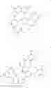
According to the invention, the injection and electron transport-facilitating effects can further be increased by the new sterically hindered donor arylboranes of substructures 1 and 2. The materials are also stable when exposed to air, not susceptible to hydrolysis, and sublimable.
The following applies:
Do is an electron donor, most suitably nitrogen, which is substituted by aromatics (phenyl or naphthyl).
R1 und R2 either form another annelated aromatic ring or
R1 forms a bridge to a donor substituent, most suitably sulfur,
R2 is in this case H or methyl.
R3 and R4 may be hydrogen or jointly form an annelated aromatic ring.
Typical electron donors are aromatic systems and any electron-rich systems like thiophenes, alkyl-substituted or sulfur-carrying, multinuclear aromatic systems, and any low electron-negative substituents, preferably electron-rich low electron-negative substituents.
The new materials capable of improving electron transport and electron injection by way of chemical interaction with any electron transporting and/or emitter layers can therefore successfully be used in any polymer-electronic components, including any technologies for the manufacture of organic light-emitting diodes (OLED's), organic field effect transistors (OFET's), and organic solar cells.
EMBODIMENTS
1)
a) Synthesis of 9-diphenylamino-anthracene through Heck coupling of diphenylamine and 9-bromoanthracene.
b) Synthesis of 10,10,10-tris-9-diphenylamino-anthryl-boran from 9-diphenylamino-anthracene, BuLi and borontribromide at −70° C.
2)
a) Synthesis of 3-methyl-1-naphthylamine per Beilstein manual 12,II,744.
b) Synthesis of 1-diphenylamino-3-methyl-naphthaline through Heck coupling from 3-methyl-1-naphthylamine and bromobenzene.
c) Synthesis of benzo-f-6-methyl-10-phenyl-phenothiazine from 1-diphenylamino-3-methyl-naphthaline and sulfur.
d) Synthesis of 7,7,7-tris-benzo-f-6-methyl-10-phenyl-phenothiazinyl-borane from benzo-f-6-methyl-10-phenyl-phenothiazine, BuLi and borontribromide at −70° C.
3)
a) Synthesis of 9-diphenylamino-anthracene through Heck coupling of diphenylamine and 9-bromoanthracene.
b) Synthesis of tetra-(9-diphenylamino-anthr-10-yl)-9,10-anthrylendiborane from 9,10-dibromoanthracene, 9-di-phenylamino-anthracene, BuLi and borotribromide at −70° C.
The invention pertains to new materials based on sterically inhibited donor arylboranes for the improvement of electron injection and electron transport in organic electronic components like organic light-emitting diodes (OLED's), organic field effect transistors (OFET's), and organic photovoltaic components, in particular solar cells.
Claims
1. Material for the n-doping of the electron-transporting layer in organic electronic components of at least one component according to one of the sterically inhibited donor arylboranes of substructures 1 and 2, including
wherein
Do represents an electron donor.
R1 and R2 form either an annelated aromatic ring or R1 forms a bridge to a donor substituent, most suitably sulfur,
R2 is in this case H or methyl,
R3 and R4 can be hydrogen or form a joint annelated aromatic ring.
2. Material according to claim 1 with Do in one of the structures 1 or 2 selected from a group of functional groups comprising nitrogen with an aromatic (phenyl or naphthyl) substituent.
3. Utilization of a material according to one of claims 1 or 2 for the n-doping of an electron-transporting layer of an organic electronic component.
4. Organic electronic component comprised of at least two electrodes with an active layer, wherein located between at least one electrode and the active layer is an electron-transporting layer doped with a material according to one of claims 1 or 2.
Images & Drawings included:


Sources:
- United States Patent and Trademark Office - verify current appl. status at the USPTO↗
Recent applications in this class:
- » 20230103127 2023-03-30
Method for enhancing stability of aggregation state of organic semiconductor film - » 20230027304 2023-01-26
Method of p-type doping carbon nanotube - » 20230022111 2023-01-26
Method of n-type doping carbon nanotube - » 20190207111 2019-07-04
Method and composition - » 20180351100 2018-12-06
N-doped semiconducting material comprising two metal dopants - » 20180233666 2018-08-16
Polymer-hybrid electro-optic devices and method of fabricating polymer-hybrid electro-optic devices - » 20170279046 2017-09-28
Doping organic semiconductors - » 20170200889 2017-07-13
Method for manufacturing transistor according to selective printing of dopant - » 20170098765 2017-04-06
Formation of films for organic photovoltaics - » 20170047517 2017-02-16
Method of fabricating an organic photodiode with dual electron blocking layers
Recent applications for this Assignee:
- » 20240045265 2024-02-08
LED backlighting system - » 20230408895 2023-12-21
LASER PROJECTION ARRANGEMENT AND METHOD FOR ARRANGING THEREOF - » 20230352617 2023-11-02
Optoelectronic semiconductor component - » 20230321970 2023-10-12
Interbonded components, method for detaching components from interbonded components, and method for producing interbonded components - » 20230265981 2023-08-24
Halogen lamp replacement - » 20230193128 2023-06-22
Phosphor compositions with orange and amber light emission - » 20230193121 2023-06-22
Quantum dot structure, method for producing a quantum dot structure, and light emitting device - » 20230174850 2023-06-08
Nanoparticle, structure, and method for producing a nanoparticle - » 20230165126 2023-05-25
Curable self-adhesive wavelength converting film and light emitting device comprising the same - » 20230163252 2023-05-25
Structure, agglomerate, optoelectronic device and methods for producing a structure and an agglomerate