Semiconductor device
US20090212357A1
2009-08-27
12/392,491
2009-02-25
✅ Patent granted
US 7,859,049 B2
2010-12-28
-
-
Phuc T Dang
2029-02-25
Abstract:
Provided is a semiconductor device. A well region (2) formed on a semiconductor substrate (1) includes a plurality of trench regions (12), and a source electrode (10) is connected to a source region (6) formed on a substrate surface between the trench regions (12). Adjacently to the source region (6), a high concentration region (11) is formed, which is brought into butting contact with the source electrode (10) together with the source region (6), whereby a substrate potential is fixed. A drain region (5) is formed at a bottom portion of the trench region (12), whose potential is taken to the substrate surface by a drain electrode (9) buried inside the trench region (12). An arbitrary voltage is applied to a gate electrode (4a, 4b), and the drain electrode (9), whereby carriers flow from the source region (6) to the drain region (5) and the semiconductor device is in an on-state.
Assignee:
- SEIKO INSTRUMENTS INC. 29 🇯🇵 Chiba-shi, Chiba, Japan
Interested in similar patents?
Get notified when new applications in this technology area are published.
Classification:
H01L29/41766 » CPC main
Semiconductor devices adapted for rectifying, amplifying, oscillating or switching, or capacitors or resistors with at least one potential-jump barrier or surface barrier, e.g. PN junction depletion layer or carrier concentration layer; Details of semiconductor bodies or of electrodes thereof; Multistep manufacturing processes therefor; Electrodes ; Multistep manufacturing processes therefor characterised by their shape, relative sizes or dispositions carrying the current to be rectified, amplified or switched; Source or drain electrodes for field effect devices with at least part of the source or drain electrode having contact below the semiconductor surface, e.g. the source or drain electrode formed at least partially in a groove or with inclusions of conductor inside the semiconductor
H01L29/41758 » CPC further
Semiconductor devices adapted for rectifying, amplifying, oscillating or switching, or capacitors or resistors with at least one potential-jump barrier or surface barrier, e.g. PN junction depletion layer or carrier concentration layer; Details of semiconductor bodies or of electrodes thereof; Multistep manufacturing processes therefor; Electrodes ; Multistep manufacturing processes therefor characterised by their shape, relative sizes or dispositions carrying the current to be rectified, amplified or switched; Source or drain electrodes for field effect devices for lateral devices with structured layout for source or drain region, i.e. the source or drain region having cellular, interdigitated or ring structure or being curved or angular
H01L29/7827 » CPC further
Semiconductor devices adapted for rectifying, amplifying, oscillating or switching, or capacitors or resistors with at least one potential-jump barrier or surface barrier, e.g. PN junction depletion layer or carrier concentration layer; Details of semiconductor bodies or of electrodes thereof; Multistep manufacturing processes therefor; Types of semiconductor device ; Multistep manufacturing processes therefor controllable by only the electric current supplied, or only the electric potential applied, to an electrode which does not carry the current to be rectified, amplified or switched; Unipolar devices, e.g. field effect transistors; Field effect transistors with field effect produced by an insulated gate Vertical transistors
H01L29/78 » CPC further
Semiconductor devices adapted for rectifying, amplifying, oscillating or switching, or capacitors or resistors with at least one potential-jump barrier or surface barrier, e.g. PN junction depletion layer or carrier concentration layer; Details of semiconductor bodies or of electrodes thereof; Multistep manufacturing processes therefor; Types of semiconductor device ; Multistep manufacturing processes therefor controllable by only the electric current supplied, or only the electric potential applied, to an electrode which does not carry the current to be rectified, amplified or switched; Unipolar devices, e.g. field effect transistors; Field effect transistors with field effect produced by an insulated gate
H01L29/76 IPC
Semiconductor devices adapted for rectifying, amplifying, oscillating or switching, or capacitors or resistors with at least one potential-jump barrier or surface barrier, e.g. PN junction depletion layer or carrier concentration layer; Details of semiconductor bodies or of electrodes thereof; Multistep manufacturing processes therefor; Types of semiconductor device ; Multistep manufacturing processes therefor controllable by only the electric current supplied, or only the electric potential applied, to an electrode which does not carry the current to be rectified, amplified or switched Unipolar devices, e.g. field effect transistors
H01L29/94 IPC
Semiconductor devices adapted for rectifying, amplifying, oscillating or switching, or capacitors or resistors with at least one potential-jump barrier or surface barrier, e.g. PN junction depletion layer or carrier concentration layer; Details of semiconductor bodies or of electrodes thereof; Multistep manufacturing processes therefor; Types of semiconductor device ; Multistep manufacturing processes therefor controllable only by variation of the electric current supplied, or only the electric potential applied, to one or more of the electrodes carrying the current to be rectified, amplified, oscillated or switched; Capacitors with potential-jump barrier or surface barrier Metal-insulator-semiconductors, e.g. MOS
H01L31/062 IPC
Semiconductor devices sensitive to infra-red radiation, light, electromagnetic radiation of shorter wavelength or corpuscular radiation and specially adapted either for the conversion of the energy of such radiation into electrical energy or for the control of electrical energy by such radiation; Processes or apparatus specially adapted for the manufacture or treatment thereof or of parts thereof; Details thereof adapted as photovoltaic [PV] conversion devices characterised by at least one potential-jump barrier or surface barrier the potential barriers being only of the metal-insulator-semiconductor type
H01L31/113 IPC
Semiconductor devices sensitive to infra-red radiation, light, electromagnetic radiation of shorter wavelength or corpuscular radiation and specially adapted either for the conversion of the energy of such radiation into electrical energy or for the control of electrical energy by such radiation; Processes or apparatus specially adapted for the manufacture or treatment thereof or of parts thereof; Details thereof in which radiation controls flow of current through the device, e.g. photoresistors characterised by at least one potential-jump barrier or surface barrier, e.g. phototransistors; Devices sensitive to infra-red, visible or ultra-violet radiation characterised by field-effect operation, e.g. junction field-effect phototransistor being of the conductor-insulator-semiconductor type, e.g. metal-insulator-semiconductor field-effect transistor
H01L31/119 IPC
Semiconductor devices sensitive to infra-red radiation, light, electromagnetic radiation of shorter wavelength or corpuscular radiation and specially adapted either for the conversion of the energy of such radiation into electrical energy or for the control of electrical energy by such radiation; Processes or apparatus specially adapted for the manufacture or treatment thereof or of parts thereof; Details thereof in which radiation controls flow of current through the device, e.g. photoresistors characterised by at least one potential-jump barrier or surface barrier, e.g. phototransistors; Devices sensitive to very short wavelength, e.g. X-rays, gamma-rays or corpuscular radiation characterised by field-effect operation, e.g. MIS type detectors
Description
RELATED APPLICATIONS
This application claims priority under 35 U.S.C. §119 to Japanese Patent Application No. JP2008-046370 filed on Feb. 27, 2008, the entire content of which is hereby incorporated by reference.
BACKGROUND OF THE INVENTION
1. Field of the Invention
The present invention relates to a semiconductor device and a method of manufacturing a semiconductor device, for example, a metal oxide semiconductor (MOS) transistor.
2. Description of the Related Art
With full use of a microfabrication technology, with times, it becomes possible to manufacture semiconductor devices while achieving downsizing without decreasing performance thereof. This tendency is also found in semiconductor elements having high driving performance, and hence a reduction in on-resistance per unit area has been pursued by making full use of the microfabrication technology. However, in fact, a lowering of a withstanding voltage, which is caused by miniaturization of elements, hinders further enhancement of the driving performance owing to the microfabrication technology. In order to overcome the trade-off between the miniaturization and the withstanding voltage, there have been proposed elements having various structures, and the trench gate MOS transistor can be nominated as a mainstream structure at present in the field of power MOS field effect transistors (FETs) having a high withstanding voltage and high driving performance.
Among doubled-diffused MOS (DMOS) transistors having a high withstanding voltage and high driving performance, the trench gate MOS transistor has the highest scale in integration (for example, see JP 01-310576 A).
The trench gate MOS transistor shows extremely excellent performance as an element itself, however it is disadvantageous when being mounted on a chip together with other semiconductor elements since the trench gate MOS transistor has a vertical MOS structure, in which current flows in a depth direction of a substrate, and an entire rear surface of a semiconductor substrate is an electrode.
SUMMARY OF THE INVENTION
The present invention has an object to provide a semiconductor device having a low on-resistance, which is capable of being mounted on a chip together with other semiconductor elements.
(1) According to the present invention, there is provided a semiconductor device including: a first conductivity type well region formed on a surface of a semiconductor substrate at an arbitrary depth; a plurality of trench regions formed at a depth smaller than the predetermined depth of the first conductivity type well region; a gate electrode disposed on a side surface of each the plurality of trench regions via a gate insulating film and brought into contact with the gate insulating film; a second conductivity type drain region formed in a bottom portion of each of the plurality of trench regions; a second conductivity type source region formed in a part of a region, which is formed between the plurality of trench regions, of the surface of the semiconductor substrate; and a first conductivity type high concentration region formed in a part of a region, which is formed between the plurality of trench regions, of the surface of the semiconductor substrate.
(2) A semiconductor device according to item (1) further includes a second conductivity type low concentration diffusion region formed between the semiconductor substrate and the first conductivity type well region to surround the second conductivity type drain region.
(3) According to the present invention, there is provided a method of manufacturing a semiconductor device including: forming a first conductivity type well region on a semiconductor substrate; forming a plurality of trench regions at a depth smaller than a depth of the first conductivity type well region; forming a gate insulating film; forming a gate electrode film; removing, by anisotropic etching, the gate insulating film and the gate electrode film formed on a bottom portion of each of the plurality of trench regions and a part of the gate insulating film and the gate electrode film formed on a surface of the semiconductor substrate between two of the plurality of trench regions; forming an interlayer insulating film; removing, by etching, a part of the interlayer insulating film formed on the gate electrode film, a part of the interlayer insulating film formed on the bottom portion of each of the plurality of trench regions, and a part of the interlayer insulating film formed on the surface of the semiconductor substrate between two of the plurality of trench regions; forming a metal film; and etching a part of the metal film.
(4) A method of manufacturing a semiconductor device according to item (3) further includes forming a second conductivity type low concentration diffusion region.
(5) A method of manufacturing a semiconductor device according to item (3) further includes performing an epitaxial growth.
According to the present invention, the drain electrode is drawn from the inside of the trench and therefore the drain electrode can be taken from the surface of the semiconductor substrate, whereby on-chip mounting with other semiconductor elements can be achieved with ease.
BRIEF DESCRIPTION OF THE DRAWINGS
In the accompanying drawings:
FIGS. 1A and 1B are views for describing a structure of a semiconductor device according to an embodiment of the present invention;
FIGS. 2A to 2F are views for describing a method of manufacturing the semiconductor device according to the embodiment of the present invention; and
FIG. 3 is a view for describing a modification example of the semiconductor device according to the embodiment of the present invention.
DETAILED DESCRIPTION OF THE PREFERRED EMBODIMENTS
(1) Outline of Embodiment
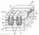
FIGS. 1A and 1B illustrate a structure of a semiconductor device according to an embodiment of the present invention. FIG. 1A is a top view, and FIG. 1B is a bird's-eye view and is cut out along a dotted-line portion of FIG. 1A.
A plurality of trench regions 12 are formed in a first conductivity type well region 2 formed on a semiconductor substrate 1. A source electrode 10 has an ohmic contact with a second conductivity type source region 6 formed on a substrate surface between the trench regions 12. Adjacently to the second conductivity type source region 6, there is formed a first conductivity type high concentration region 11, which is brought into butting contact with the source electrode 10 together with the second conductivity type source region 6, whereby a substrate potential is fixed.
A second conductivity type drain region 5 is formed at a bottom portion of the trench region 12, and a potential is taken to the substrate surface by a drain electrode 9 buried inside the trench region 12.
An arbitrary voltage is applied to the drain electrode 9 and a gate electrode 4b made of metal which is connected to a gate electrode 4a formed continuously over a flat region on an outer side of the trench region 12 and a side wall inside the trench region 12, whereby carriers flow from the second conductivity type source region 6 to the second conductivity type drain region 5 in a direction indicated with an arrow 8, bringing the semiconductor device into an on-state.
Specifically, as in a trench MOS transistor, a gate length extends in a direction perpendicular to the surface of the semiconductor substrate, and hence an area efficiency is excellent compared with a planar type MOS transistor, resulting in enhancement of driving performance per unit area. Further, all the electrodes are exposed to the surface of the semiconductor substrate, and therefore on-chip mounting with other elements, which has been difficult to be achieved in the trench MOS transistor, is realized with ease.
Next, a method of manufacturing the semiconductor device is described.
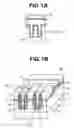
FIGS. 2A to 2F are bird's-eye views of a process flow, illustrating the method of manufacturing the semiconductor device according to the basic embodiment of the present invention illustrated in FIGS. 1A and 1B.
First, as illustrated in FIG. 2A, the first conductivity type well region 2 is formed on the semiconductor substrate 1 and then the trench regions 12 are formed in the first conductivity type well region 2 at a depth smaller than that of the first conductivity type well region 2. After that, thermal oxidation is performed to form a gate oxide film 3 on the substrate surface and inside the trench regions 12.
Next, as illustrated in FIG. 2B, the gate electrode film 4a is deposited on the gate oxide film 3 and, as illustrated in FIG. 2C, the gate electrode film 4a and the gate oxide film 3 are partially removed by highly anisotropic dry etching. In this case, as to the substrate surface and a trench bottom surface included in a region to be etched, the gate electrode film 4a and the gate oxide film 3 are all removed, but the gate electrode film 4a and the gate oxide film 3 deposited on a trench side wall are not removed by highly anisotropic dry etching.
As illustrated in FIG. 2D, second conductivity type impurities are ion-implanted into a region excluding a region in which the first conductivity type high concentration region 11 is formed so that the second conductivity type drain region 5 and the second conductivity type source region 6 are formed in a self-aligning manner. After that, the region excluding the region in which the first conductivity type high concentration region 11 is formed is masked with a resist or the like, whereby the first conductivity type high concentration region 11 is formed by ion-implantation or the like.
Next, as illustrated in FIG. 2E, an interlayer insulating film 7 is deposited. Thereafter, the interlayer insulating film 7 is subjected to selective etching in a part of regions of the second conductivity type drain region 5, the second conductivity type source region 6, the first conductivity type high concentration region 11, and the gate electrode 4a to thereby form openings.
Finally, as illustrated in FIG. 2F, metal is deposited to be arbitrarily patterned, whereby the gate electrode 4b, the drain electrode 9, and the source electrode 10 are formed.
MODIFICATION EXAMPLE
In this modification example, an electric field relaxation region is formed in a drain region, whereby a withstanding voltage of a semiconductor device is enhanced.
FIG. 3 is a conceptual view of the modification example. FIG. 3 illustrates a structure in which, in the basic structure of FIGS. 1A and 1B, a second conductivity type low concentration diffusion region 13 is formed between the semiconductor substrate 1 and the first conductivity type well region 2. This structure is realized by a manufacturing method such as a double diffusion or an epitaxial growth.
As described above, the second conductivity type low concentration diffusion region 13 is formed, whereby an electric field applied to a drain can be mitigated and a drain withstanding voltage can be enhanced.
In this case, the second conductivity type drain region 5 is set so as to be within the second conductivity type low concentration diffusion region 13, and a impurity concentration of the second conductivity type low concentration diffusion region 13 and a distance between the deepest bottom portion of the trench region 12 and a bottom portion of the first conductivity type well region 2 are arbitrarily adjusted based on a target withstanding voltage.
Note that, in FIGS. 1A and 1B, 2A to 2F, and 3, the first conductivity type is set to p-type, and the second conductivity type is set to n-type, whereby the n-channel MOS transistor is described. When the first conductivity type is set to n-type and the second conductivity type is set to p-type, this transistor functions as a p-channel MOS transistor.
Claims
What is claimed is:1. A semiconductor device, comprising:
a first conductivity type well region disposed on a surface of a semiconductor substrate at a predetermined depth;
a plurality of trench regions disposed at a depth smaller than the predetermined depth of the first conductivity type well region;
a gate electrode disposed on a side surface of each of the plurality of trench regions via a gate insulating film and brought into contact with the gate insulating film;
a second conductivity type drain region disposed in a bottom portion of each of the plurality of trench regions;
a second conductivity type source region disposed in a region formed between the plurality of trench regions, and disposed on the surface of the semiconductor substrate along the gate insulating film; and
a first conductivity type high concentration region disposed in a region formed between the plurality of trench regions, and disposed on the surface of the semiconductor substrate to be brought into contact with the second conductivity type source region.
2. A semiconductor device according to claim 1, further comprising a second conductivity type low concentration diffusion region formed between the semiconductor substrate and the first conductivity type well region to surround the second conductivity type drain region.
3. A method of manufacturing a semiconductor device, comprising:
forming a first conductivity type well region on a semiconductor substrate;
forming a plurality of trench regions at a depth smaller than a depth of the first conductivity type well region;
forming a gate insulating film;
forming a gate electrode film;
removing, by anisotropic etching, the gate insulating film and the gate electrode film formed on a bottom portion of each of the plurality of trench regions and a part of the gate insulating film and the gate electrode film formed on a surface of the semiconductor substrate between two of the plurality of trench regions;
forming an interlayer insulating film;
removing, by etching, a part of the interlayer insulating film formed on the gate electrode film, a part of the interlayer insulating film formed on the bottom portion of each of the plurality of trench regions, and a part of the interlayer insulating film formed on the surface of the semiconductor substrate between two of the plurality of trench regions;
forming a metal film; and
etching a part of the metal film.
4. A method of manufacturing a semiconductor device according to claim 3, further comprising forming, before the forming the first conductivity type well region on the semiconductor substrate, a second conductivity type low concentration diffusion region on an entire surface of a region on which a transistor is formed.
5. A method of manufacturing a semiconductor device according to claim 4, wherein the forming the second conductivity type low concentration diffusion region on the entire surface of the region on which the transistor is formed comprises an epitaxial growth.
Images & Drawings included:


Sources:
- United States Patent and Trademark Office - verify current appl. status at the USPTO↗
Similar patent applications:
- » 20110037176
METHOD OF MANUFACTURING A SEMICONDUCTOR DEVICE MODULE, SEMICONDUCTOR DEVICE CONNECTING DEVICE, SEMICONDUCTOR DEVICE MODULE MANUFACTURING DEVICE, SEMICONDUCTOR DEVICE MODULE - » 20230162992
METHOD FOR MANUFACTURING SEMICONDUCTOR DEVICE, METHOD FOR MANUFACTURING DEVICE PROVIDED WITH SEMICONDUCTOR DEVICE, SEMICONDUCTOR DEVICE, AND DEVICE PROVIDED WITH SEMICONDUCTOR DEVICE - » 10889015
Attaching device for mounting and fixing a semiconductor device and a heat sink provided on the semiconductor device on a board, a mount board having the board, the semiconductor device, and the heat sink, and an attaching method of the semiconductor device and the heat sink provided on the semiconductor device on the board - » 20130062745
Semiconductor device, semiconductor device manufacturing method, semiconductor device mounting structure and power semiconductor device - » 20070001197
SEMICONDUCTOR DEVICE, SEMICONDUCTOR DEVICE DESIGN METHOD, SEMICONDUCTOR DEVICE DESIGN METHOD RECORDING MEDIUM, AND SEMICONDUCTOR DEVICE DESIGN SUPPORT SYSTEM - » 10600737
Semiconductor device, semiconductor device design method, semiconductor device design method recording medium, and semiconductor device design support system - » 20130168734
Epitaxial substrate for semiconductor device, semiconductor device, method of manufacturing epitaxial substrate for semiconductor device, and method of manufacturing semiconductor device - » 20110266660
Insulating film for semiconductor device, process and apparatus for producing insulating film for semiconductor device, semiconductor device, and process for producing the semiconductor device - » 20130207111
SEMICONDUCTOR DEVICE, DISPLAY DEVICE INCLUDING SEMICONDUCTOR DEVICE, ELECTRONIC DEVICE INCLUDING SEMICONDUCTOR DEVICE, AND METHOD FOR MANUFACTURING SEMICONDUCTOR DEVICE - » 20170338352
Semiconductor device, display device including semiconductor device, electronic device including semiconductor device, and method for manufacturing semiconductor device
Recent applications in this class:
- » 20250072087 2025-02-27
SEMICONDUCTOR DEVICE AND METHOD OF FABRICATING THE SAME - » 20250056865 2025-02-13
SEMICONDUCTOR DEVICE BACKSIDE ISOLATION FEATURE INTEGRATION - » 20250056864 2025-02-13
SEMICONDUCTOR STRUCTURE WITH ENHANCED PLACEHOLDER POSITION MARGIN - » 20250031430 2025-01-23
EXTENDED BACKSIDE CONTACT IN STACK NANOSHEET - » 20250022927 2025-01-16
SEMICONDUCTOR DEVICE AND ELECTRONIC APPARATUS INCLUDING THE SAME - » 20250015152 2025-01-09
NITRIDE SEMICONDUCTOR DEVICE - » 20250015151 2025-01-09
SEMICONDUCTOR DEVICE - » 20240429294 2024-12-26
INTEGRATED CIRCUIT STRUCTURE WITH BACKSIDE PLUG LAST APPROACH - » 20240421203 2024-12-19
SEMICONDUCTOR DEVICE - » 20240421202 2024-12-19
FEEDTHROUGH VIA BETWEEN ACTIVE REGIONS
Recent applications for this Assignee:
- » 20180311978 2018-11-01
Thermal printer and portable terminal - » 20180238685 2018-08-23
Tilt sensor - » 20170292877 2017-10-12
Cantilever pressure sensor with division portions for dividing lever resistance and having piezoresistor element - » 20170131168 2017-05-11
Pressure sensor - » 20160268558 2016-09-15
Nonaqueous electrolyte secondary battery - » 20160268060 2016-09-15
Electrochemical cell and electrochemical cell with terminal - » 20150364464 2015-12-17
Semiconductor device - » 20150342476 2015-12-03
ELECTRONIC APPARATUS AND PROGRAM - » 20150096388 2015-04-09
Pressure sensor having cantilever and displacement measurement unit - » 20130326234 2013-12-05
Information processing device and information processing program