PHOTOVOLTAIC DEVICE
US20090260679A1
2009-10-22
12/339,379
2008-12-19
Abstract:
A photovoltaic device includes a substrate, a doped layer, a first electrode and a second electrode. The substrate has a plurality of cavities defined therein. The doped layer is in contact the substrate. The first electrode including a carbon nanotube composite material is adjacent to the substrate. The second electrode is attached to the substrate.
Inventors:
- SHOU-SHAN FAN 1,480 🇨🇳 Beijing, China
- KAI-LI JIANG 696 🇨🇳 Beijing, China
- QUN-QING LI 325 🇨🇳 Beijing, China
- HAI-LIN SUN 13 🇨🇳 Beijing, China
Assignee:
- HON HAI PRECISION INDUSTRY CO., LTD. 12,828 🇹🇼 Tu-Cheng, Taiwan
- Tsinghua University 3,008 🇨🇳 Beijing, China
Interested in similar patents?
Get notified when new applications in this technology area are published.
Classification:
H01L31/0236 » CPC main
Semiconductor devices sensitive to infra-red radiation, light, electromagnetic radiation of shorter wavelength or corpuscular radiation and specially adapted either for the conversion of the energy of such radiation into electrical energy or for the control of electrical energy by such radiation; Processes or apparatus specially adapted for the manufacture or treatment thereof or of parts thereof; Details thereof; Details Special surface textures
B82Y20/00 » CPC further
Nanooptics, e.g. quantum optics or photonic crystals
G02B6/1226 » CPC further
Light guides of the optical waveguide type of the integrated circuit kind; Basic optical elements, e.g. light-guiding paths involving surface plasmon interaction
H01L31/022425 » CPC further
Semiconductor devices sensitive to infra-red radiation, light, electromagnetic radiation of shorter wavelength or corpuscular radiation and specially adapted either for the conversion of the energy of such radiation into electrical energy or for the control of electrical energy by such radiation; Processes or apparatus specially adapted for the manufacture or treatment thereof or of parts thereof; Details thereof; Details; Electrodes for devices characterised by at least one potential jump barrier or surface barrier for solar cells
H01L31/022466 » CPC further
Semiconductor devices sensitive to infra-red radiation, light, electromagnetic radiation of shorter wavelength or corpuscular radiation and specially adapted either for the conversion of the energy of such radiation into electrical energy or for the control of electrical energy by such radiation; Processes or apparatus specially adapted for the manufacture or treatment thereof or of parts thereof; Details thereof; Details; Electrodes made of transparent conductive layers, e.g. TCO, ITO layers
H01L31/03529 » CPC further
Semiconductor devices sensitive to infra-red radiation, light, electromagnetic radiation of shorter wavelength or corpuscular radiation and specially adapted either for the conversion of the energy of such radiation into electrical energy or for the control of electrical energy by such radiation; Processes or apparatus specially adapted for the manufacture or treatment thereof or of parts thereof; Details thereof characterised by their semiconductor bodies characterised by their shape or by the shapes, relative sizes or disposition of the semiconductor regions characterised by at least one potential jump barrier or surface barrier Shape of the potential jump barrier or surface barrier
H01L31/068 » CPC further
Semiconductor devices sensitive to infra-red radiation, light, electromagnetic radiation of shorter wavelength or corpuscular radiation and specially adapted either for the conversion of the energy of such radiation into electrical energy or for the control of electrical energy by such radiation; Processes or apparatus specially adapted for the manufacture or treatment thereof or of parts thereof; Details thereof adapted as photovoltaic [PV] conversion devices characterised by at least one potential-jump barrier or surface barrier the potential barriers being only of the PN homojunction type, e.g. bulk silicon PN homojunction solar cells or thin film polycrystalline silicon PN homojunction solar cells
Y02E10/547 » CPC further
Energy generation through renewable energy sources; Photovoltaic [PV] energy Monocrystalline silicon PV cells
Y02E10/547 » CPC further
Energy generation through renewable energy sources; Photovoltaic [PV] energy Monocrystalline silicon PV cells
H01L31/00 IPC
Semiconductor devices sensitive to infra-red radiation, light, electromagnetic radiation of shorter wavelength or corpuscular radiation and specially adapted either for the conversion of the energy of such radiation into electrical energy or for the control of electrical energy by such radiation; Processes or apparatus specially adapted for the manufacture or treatment thereof or of parts thereof; Details thereof
Description
BACKGROUND
1. Technical Field
The invention relates to energy conversion devices, and particularly to a photovoltaic device.
2. Description of Related Art
Currently, solar energy is considered a renewable and clean alternative energy source. Solar energy is generally produced by photovoltaic cells, also known as solar cells. The solar cell is a device that converts light into electrical energy using the photoelectric effect.
Generally, the solar cell includes a large-area p-n junction made from silicon. Silicon employed in the solar cell can be single crystal silicon or polycrystalline silicon. Referring to FIG. 4, a conventional solar cell 30 according to the prior art generally includes a silicon substrate 32, a doped silicon layer 34, a front electrode 36, and a rear electrode 38. The doped silicon layer 34 is in contact with the silicon substrate 32 to form a p-n junction. The front electrode 36 is disposed on and electrically connected to the doped silicon layer 34. The rear electrode 38 is disposed on and electrically connected to, e.g. via ohmic contact, the silicon substrate 32. In use, the electrodes 36, 38 are connected to an external load. Current will be generated and flow in one direction across the p-n junction by the action of the electric field if light strikes the solar cell 30.
Generally, the electrodes 36, 38 are made of conductive metals, such as aluminum (Al), silver (Ag) or copper (Cu), which are usually not transparent to light. Therefore, the electrode 36, 38, in particular, the front electrode 36 is fabricated in a finger-shape or a comb-shape to increase amount of incoming light that can pass by the electrode. Moreover, in order to enhance photoelectric conversion efficiency, transparent conductive material, e.g. indium tin oxide (ITO), may instead be selected to form the front electrode 36. However, ITO material has drawbacks, for example, ITO is known not to be chemically and mechanically durable, and as having uneven distribution of resistance. As a result, the durability and the photoelectric conversion efficiency are relatively low for devices using transparent conductive materials such as ITO.
What is needed, therefore, is a photovoltaic device that is more efficient and durable.
BRIEF DESCRIPTION OF THE DRAWINGS
The components in the drawing are not necessarily drawn to scale, the emphasis instead being placed upon clearly illustrating the principles of the present invention.
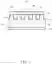
FIG. 1 is a schematic lateral view showing a photovoltaic device in accordance with an exemplary embodiment.
FIG. 2 is a schematic view showing a first electrode of the photovoltaic device of FIG. 1.
FIG. 3 is a schematic view showing one portion of carbon nanotubes in a form of film according to an exemplary embodiment.
FIG. 4 is a schematic view of a conventional solar cell according to the prior art.
Corresponding reference characters indicate corresponding parts throughout the drawings. The exemplifications set out herein illustrate at least one embodiment of the present photovoltaic device, in one form, and such exemplifications are not to be construed as limiting the scope of the disclosure in any manner.
DETAILED DESCRIPTION OF THE EMBODIMENT
Reference will now be made to the drawings to describe embodiments of the present photovoltaic device in detail.
Referring to FIG. 1, a photovoltaic device 10 according to an exemplary embodiment, is shown. The photovoltaic device 10 includes a substrate 12, a doped layer 14, a first electrode 16, and a second electrode 18.
The substrate 12 can be made of single crystal silicon. In the exemplary embodiment, the substrate 12 is p-type single crystal silicon. In addition, a thickness of the substrate 12 is in a range from about 200 μm to about 300 μm. The substrate 12 has a front surface 121 and a rear surface 122, as shown in FIG. 1. The front surface 121 of the substrate 12 defines a plurality of cavities 123. That is, some portions of the front surface 121 form the cavities 123 for enhancing light collation and increasing the area of p-n junction formation. The cavities 123 are distributed evenly and are spaced from each other by a distance in a range from about 10 μm to about 30 μm. In addition, a depth of each of the cavities 123 is in a range from about 50 μm to about 70 μm. However, in other embodiments, the cavities 123 may vary in shape and dimension. While a square cross section is shown, the cross section of each of the cavities 123 can be, for example, square, trapezoidal, triangular, circular or other shapes.
The doped layer 14 is disposed on inside walls of each cavity 123. In the exemplary embodiment, the doped layer 14 is n-type silicon made by adding an abundance of dopant, such as phosphorus (P) or arsenic (As), into the substrate 12. In addition, a thickness of the doped layer 14 is in a range from about 500 nm to about 1 μm. Thus, a plurality of p-n junctions are formed where the n-type doped layer 14 and the p-type single crystal substrate 12 meet, achieving light radiation to electrical energy conversions.
The first electrode 16 is adjacent to the front surface 121 of the substrate 12. The second electrode 18 is attached to the rear surface 122 of the substrate 12. The second electrode 18 can be made of aluminum (Al), magnesium (Mg), or silver (Ag), and has a thickness ranging from 10 μm to 300 μm.
Referring to FIG. 1 and FIG. 2, the first electrode 16, which includes a carbon nanotube (CNT) composite material, is configured for collecting current generated at the p-n junctions based on photoelectric conversion. The composite material includes a plurality of CNTs 161 and a plurality of metal particles 163 dispersed in the CNTs. In the exemplary embodiment, the metal particles 163 are evenly dispersed in the CNT composite material. The metal particles 163 can be selected from the group consisting of platinum (Pt), palladium (Pd), ruthenium (Ru), silver (Ag), gold (Au), alloys and combinations thereof. An average particle diameter of the metal particles 163 is in a range from about 1 nm to about 10 nm. A percentage by mass of the metal particles 163 in the CNT composite material is in a range from about 10% to about 30%.
In the exemplary embodiment, the CNTs 161 can be selected from a group consisting of single-walled CNTs (SWCNTs), double-walled CNTs, multi-walled CNTs (MWCNTs), and combinations thereof. When the SWCNTs are employed in the first electrode 16, a diameter of each of the SWCNTs is in a range from about 0.5 nm to about 50 nm. When the double-walled CNTs are employed in the first electrode 16, a diameter of each of the double-walled CNTs is in a range from about 1.0 nm to about 50.0 nm. Alternatively, when the MWCNTs are employed in the first electrode 16, a diameter of each of the MWCNTs is in a range from about 1.5 nm to about 50.0 nm. In the exemplary embodiment, the first electrode 16 made of CNT composite material can be directly adhered on the front surface 121 of the substrate 12 due to the adhesiveness of the CNTs 161. In the exemplary embodiment, a percentage by mass of the CNTs 161 in the CNT composite material is in a range from about 70% to about 90%.
In the exemplary embodiment, the CNTs 161 can be arranged orderly or disorderly. In addition, the CNTs 161 can be in a form of at least one film, as shown in FIG. 2. The film can be fabricated by being drawn from a CNT array, which may be formed on a 4-inch silicon by vapor deposition. Referring to FIG. 3, the film includes a plurality of successively oriented CNT segments 160 joined end-to-end by van der Waals attractive force. Each CNT segment 160 comprises a plurality of CNTs substantially parallel to each other and with the same length. In the exemplary embodiment, a width of the film is in a range of about 0.01 cm to about 10.00 cm. A thickness of the film is in a range of about 10 nm to 100 μm. Referring to FIG. 2, the film defines a plurality of spaces S that allow relatively greater amount of incoming light to penetrate into the silicon substrate 12. The metal particles 163 can be dispersed on the film, as shown in FIG. 2.
In the film having ordered CNTs 161, the CNTs 161 are arranged along and parallel to a surface of the film. In addition, the CNTs 161 are oriented along one direction. Alternatively, the CNTs 161 can be oriented along different directions, e.g. two directions perpendicular to each other. In the film having disordered CNTs 161, the CNTs 161 entangle with each other or are arranged in an isotropic fashion.
In other embodiments, the CNTs 161 can be in the form of two or more stacked films. The alignment direction of CNTs 161 of two adjacent films, or sets of films, can be set at an angle α to each other. The angle α is in a range of 0<α≦90°. It is noted that the number of the films can be chosen according to practical requirements, forming different thickness of the first electrode 16. In the exemplary embodiment, there are two films set at an angle of 90 degrees, as seen in FIG. 2.
The length and width of the film is only limited by the size of the CNT array. Furthermore, the CNTs of the film, which are joined end-to-end, with the same length and arranged substantially uniform, provide the photovoltaic device 10 with a substantially uniform distribution of resistance. The spaces S defined on the film also provide the photovoltaic device 10 with better light transmission. A first electrode 16 made with CNTs has improved mechanical strength and durability by virtue of the CNTs.
In use, when light strikes on the photovoltaic device 10, one portion of incoming light passes through the spaces S and is incident into the cavities 123 while the other portion of incoming light shines on the first electrode 16. For the portion of incoming light passing through the spaces S, the light will be trapped through multiple reflections within the cavities 123. The light absorption is increased and the photovoltaic device 10 has greatly enhanced efficiency.
For the portion of incoming light shining on the first electrode 16, surface plasmons are observed on the metal particles 163 as light shines onto the surfaces of metal particles 163 of the first electrode 16. The surface plasmons can then be excited by the light and interact with the light to result in a polariton. A phenomenon of surface plasmon resonance is generated, i.e. surface plasmons are excited to be in resonance with the incoming light of a predetermined frequency. By way of the surface plasmon resonance on the metal particles 163, the incoming light again irradiates from the metal particles 163 and is incident into the cavities 123. As a result, the absorption of light for the photovoltaic device 10 is increased.
Furthermore, the photovoltaic device 10 of the exemplary embodiment can further include an anti-reflection layer 22 disposed on the first electrode 16. The anti-reflection layer 22 is configured to reduce light striking on the first electrode 16 to reflect, causing the energy conversion efficiency to be enhanced. In the exemplary embodiment, the anti-reflection layer 22 is made of titanium dioxide or zinc aluminum oxide.
In exemplary embodiment, the photovoltaic device 10 further includes at least one third electrode 20 electrically connected to the first electrode 16 for collecting current flowing through the first electrode 16.
Finally, it is to be understood that the above-described embodiments are intended to illustrate rather than limit the invention. Variations may be made to the embodiments without departing from the spirit of the invention as claimed. The above-described embodiments illustrate the scope of the invention but do not restrict the scope of the invention.
Claims
What is claimed is:1. A photovoltaic device, comprising:
a substrate having a plurality of cavities defined therein;
a doped layer in contact the substrate;
a first electrode comprising a carbon nanotube composite material adjacent to the substrate; and
a second electrode attached to the substrate.
2. The photovoltaic device as claimed in claim 1, wherein the substrate comprises p-type silicon.
3. The photovoltaic device as claimed in claim 1, wherein a thickness of the substrate is in a range from about 200 μm to about 300 μm.
4. The photovoltaic device as claimed in claim 1, wherein the cavities are spaced from each other by a distance in a range from about 10 μm to about 30 μm.
5. The photovoltaic device as claimed in claim 1, wherein a depth of each of the cavities is in a range from about 50 μm to about 70 μm.
6. The photovoltaic device as claimed in claim 1, wherein the doped layer comprises n-type silicon.
7. The photovoltaic device as claimed in claim 1, wherein the carbon nanotube composite material comprises of a plurality of carbon nanotubes and a plurality of metal particles.
8. The photovoltaic device as claimed in claim 7, wherein each metal particle comprises of a material that is selected from the group consisting of platinum, palladium, ruthenium, silver, gold, and any alloy thereof.
9. The photovoltaic device as claimed in claim 7, wherein the metal particles have an average particle diameter in a range from about 1 nm to about 10 nm.
10. The photovoltaic device as claimed in claim 7, wherein the carbon nanotubes are arranged in a disorderly fashion.
11. The photovoltaic device as claimed in claim 7, wherein at least a portion of the carbon nanotubes are in a form of at least one film.
12. The photovoltaic device as claimed in claim 11, wherein the at least one film comprises of a plurality of successively oriented carbon nanotube segments joined end-to-end by van der Waals attractive force.
13. The photovoltaic device as claimed in claim 12, wherein each carbon nanotube segment comprises a plurality of carbon nanotubes substantially parallel to each other and with the same length.
14. The photovoltaic device as claimed in claim 11, wherein there are two or more stacked films.
15. The photovoltaic device as claimed in claim 14, wherein the carbon nanotubes of the adjacent films are set at an angle ranging from about 0 degrees to about 90 degrees.
16. The photovoltaic device as claimed in claim 1, further comprising a third electrode electrically connected to the first electrode.
17. The photovoltaic device as claimed in claim 1, further comprising an anti-reflection layer disposed on the first electrode.
18. The photovoltaic device as claimed in claim 17, wherein the anti-reflection layer comprises of titanium dioxide or zinc aluminum oxide.
Images & Drawings included:


Sources:
- United States Patent and Trademark Office - verify current appl. status at the USPTO↗
Similar patent applications:
- » 20090007955
Photovoltaic Device, Photovoltaic Module Comprising Photovoltaic Device, and Method for Manufacturing Photovoltaic Device - » 20180120483
Light Condensing Device, Photovoltaic Device, Light Condensing Sheet, Photovoltaic Sheet, and Method for Manufacturing Light Condensing Device or Photovoltaic Device - » 20100006154
Electron donating organic material for photovoltaic devices, material for photovoltaic devices, and photovoltaic device - » 20110204292
COMPOSITIONS FOR FORMING WAVELENGTH CONVERSION FILMS FOR PHOTOVOLTAIC DEVICES, WAVELENGTH CONVERSION FILMS FOR PHOTOVOLTAIC DEVICES, AND PHOTOVOLTAIC DEVICES - » 20200227574
Photovoltaic device, solar cell string of photovoltaic devices, and solar cell module including either photovoltaic device or solar cell string - » 20120167970
METHOD FOR PRODUCING A LIGHT TRAPPING LAYER ON A TRANSPARENT SUBSTRATE FOR USE IN A PHOTOVOLTAIC DEVICE, A METHOD FOR PRODUCING A PHOTOVOLTAIC DEVICE AS WELL AS SUCH A PHOTOVOLTAIC DEVICE - » 20190323733
MOUNTING DEVICE FOR PHOTOVOLTAIC DEVICE AND PHOTOVOLTAIC DEVICE ASSEMBLY - » 20130284233
Photovoltaic device, photovoltaic system, and vehicle including photovoltaic device - » 20180006168
Photovoltaic device, photovoltaic module, and method for fabricating the photovoltaic device - » 20110023964
Electron donating material, material for photovoltaic devices and photovoltaic device
Recent applications in this class:
- » 20240079509 2024-03-07
SOLAR CELL, AND TEXTURED SURFACE STRUCTURE AND METHOD FOR PREPARING SAME - » 20240021742 2024-01-18
Solar cell and method for manufacturing solar cell - » 20230420584 2023-12-28
SINGLE-PHOTON DETECTION ELEMENT, ELECTRONIC DEVICE, AND LiDAR DEVICE - » 20220190172 2022-06-16
LASER-TEXTURED THIN-FILM SEMICONDUCTORS BY MELTING AND ABLATION - » 20210119065 2021-04-22
Optoelectronic device with reflective face - » 20200321480 2020-10-08
Laser-textured thin-film semiconductors by melting and ablation - » 20200028000 2020-01-23
Microstructure enhanced absorption photosensitive devices - » 20190123216 2019-04-25
Photovoltaic structure for a roadway - » 20190019899 2019-01-17
Microstructure enhanced absorption photosensitive devices - » 20180006164 2018-01-04
Opto-electronic device with textured surface and method of manufacturing thereof
Recent applications for this Assignee:
- » 20250150619 2025-05-08
DATA STORAGE METHOD, READING METHOD, APPARATUS, STORAGE MEDIUM, AND PROGRAM PRODUCT - » 20250149667 2025-05-08
METHOD OF TARGETED RECYCLING OF WASTE BATTERIES - » 20250133304 2025-04-24
EVENT DATA PROCESSING METHOD AND RELATED DEVICE - » 20250105632 2025-03-27
DAY-AHEAD SCHEDULING METHOD AND APPARATUS FOR POWER SYSTEM, ELECTRONIC DEVICE AND STORAGE MEDIUM - » 20250096469 2025-03-20
PLANAR INVERTED F ANTENNA PAIR AND ELECTRONIC DEVICE - » 20250096324 2025-03-20
ELECTROLYTIC SOLUTION FOR RECHARGEABLE MAGNESIUM BATTERIES, METHOD FOR PREPARING THE SAME, AND RECHARGEABLE MAGNESIUM BATTERIES - » 20250095728 2025-03-20
COMPUTING APPARATUS AND ROBUSTNESS PROCESSING METHOD THEREFOR - » 20250094818 2025-03-20
DATA DENOISING METHOD AND RELATED DEVICE - » 20250088152 2025-03-13
RADIO FREQUENCY AMPLIFICATION CIRCUIT, RADIO FREQUENCY TRANSCEIVER, AND COMMUNICATION DEVICE - » 20250086928 2025-03-13
IMAGE PROCESSING METHOD AND IMAGE PROCESSING APPARATUS FOR RECOGNIZING TARGET OBJECT