Electronic ballast
US20100102742A1
2010-04-29
12/588,639
2009-10-22
✅ Patent granted
US 8,164,280 B2
2012-04-24
-
-
Douglas W Owens | Thai Pham
2030-08-28
Abstract:
Provided is an electronic ballast including: a rectifier which rectifies alternating current (AC) power into direct current (DC) power; a power factor compensator which improves a power face of the DC power; an inverter which inverts the DC current into high frequency square wave power; and a resonant circuit which receives the high frequency square wave power from the inverter, adjusts impedance, transforms the high frequency square wave power into high frequency sine wave power, and outputs the high frequency sine wave power.
Assignee:
- FEELUX CO., LTD. 9 🇰🇷 Gyeonggi-do, South Korea
- FEELUX Co., Ltd. 3 🇰🇷 Kyonggi-do, South Korea
Interested in similar patents?
Get notified when new applications in this technology area are published.
Classification:
H05B41/2885 » CPC main
Circuit arrangements or apparatus for igniting or operating discharge lamps; Circuit arrangements in which the lamp is fed by power derived from dc by means of a converter, e.g. by high-voltage dc using static converters with semiconductor devices and specially adapted for lamps without preheating electrodes, e.g. for high-intensity discharge lamps, high-pressure mercury or sodium lamps or low-pressure sodium lamps Static converters especially adapted therefor; Control thereof
H05B41/42 » CPC further
Circuit arrangements or apparatus for igniting or operating discharge lamps; Circuit arrangements; Controlling; Controlling the intensity of light discontinuously in two steps only
Y02B20/00 » CPC further
Energy efficient lighting technologies, e.g. halogen lamps or gas discharge lamps
Y02B20/00 » CPC further
Energy efficient lighting technologies, e.g. halogen lamps or gas discharge lamps
H05B41/26 IPC
Circuit arrangements or apparatus for igniting or operating discharge lamps; Circuit arrangements in which the lamp is fed by power derived from dc by means of a converter, e.g. by high-voltage dc
Description
CROSS-REFERENCE TO RELATED PATENT APPLICATION
This application claims the benefit of Korean Patent Application No. 10-2008-0104724, filed on Oct. 24, 2008, in the Korean Intellectual Property Office, the disclosure of which is incorporated herein in its entirety by reference.
BACKGROUND OF THE INVENTION
1. Field of the Invention
The present invention relates to an electronic ballast, and more particularly, to an electronic ballast for varying an inductor or a capacitor of a resonance circuit according to a selection of a user in order to adjust consumed power of a lamp.
2. Description of the Related Art
A fluorescent lamp is a kind of discharge tubes and requires a high voltage on an initial stage to discharge thermal electrons necessary for electric discharge. Also, the fluorescent lamp has a negative resistance characteristic in which a voltage applied thereto after the electric discharge decreases with an increase in a current flowing in the fluorescent lamp. Therefore, the fluorescent lamp is unstably lighted or broken down due to the negative resistance characteristic. An electronic ballast supplies a high voltage to the fluorescent lamp on the initial stage to light the fluorescent lamp and then controls the current flowing in the fluorescent lamp to keep the brightness of the fluorescent lamp constant.
Since a magnetic ballast uses a chock coil, a leakage transformer, and a high capacity condenser, the magnetic ballast loses a large amount of power of about 8 W due to light emitted from a fluorescent lamp and heat generated by an iron core and a copper wire. Thus, power of about 8 W or more is lost. Also, since the magnetic ballast lights the fluorescent lamp with commonly used power of 60 Hz, the fluorescent lamp flickers. When a power state is poor and the magnetic ballast is worn out, the fluorescent lamp may more seriously flicker and may not be lighted up at a low ambient temperature or a high percentage of humidity.
In order to solve these problems, the electronic ballast rectifies commonly used alternating current (AC) power of 60 Hz into direct current (DC) power using a semiconductor device. Also, an inverter circuit converts the DC power into high frequency power between 25 KHz and 50 KHz so as to stably light the fluorescent lamp through an output power controlling circuit. Since the electronic ballast lights the fluorescent lamp using the high frequency power, the electronic ballast improves luminous efficiency by about 15%, compared to the magnetic ballast. Also, since the electronic ballast uses the semiconductor device, the electronic ballast reduces loss of power caused by heat generated from the chock coil by about 25%. Thus, the electronic ballast a power saving effect of 35% or more, compared to the magnetic ballast.
Besides saving power, the electronic ballast lights the fluorescent lamp (which flickers 5 to 10 million times per second) using the high frequency power to supply high-quality light sensed by eyes so as to protect eyesight. In addition, the electronic ballast removes noise which is generated by vibrations of an electromagnetic force generated by the chock coil and the iron core of the magnetic ballast. The electronic ballast is lighter than the magnetic ballast and generates heat 10° lower than the magnetic ballast. Thus, the electronic ballast reduces a heating rate. Since the electronic ballast lights the fluorescent lamp even at a low voltage, the electronic ballast is appropriate in the summer in which a power state is poor or in a region in which a power state is poor. Also, the electronic ballast lights the fluorescent lamp at a low temperature and uses lamps without distinction.
The above contents have been described to help understanding of the present invention but do not mean the prior art widely well known in the art to which the present invention pertains.
SUMMARY OF THE INVENTION
As described above, an electronic ballast may minimize a reduction in energy efficiency caused by loss of heat and loss of power caused by a decrease in a power factor, compared to a magnetic ballast. Thus, the electronic ballast may efficiently save power. However, the electronic ballast generates constant power and thus cannot control power varying according to a selection of a user. Thus, the electronic ballast may not save power of a product in which the electronic ballast is installed. As a result, these disadvantages of the electronic ballast are required to be solved.
Accordingly, in order to solve the above problems, the present invention provides an electronic ballast for varying an inductor or a capacitor of a resonant circuit according to a selection of a user to adjust consumed power of a lamp so as to more efficiently control a power saving effect.
According to an aspect of the present invention, there is provided an electronic ballast including: a rectifier which rectifies alternating current (AC) power into direct current (DC) power; a power factor compensator which improves a power face of the DC power; an inverter which inverts the DC current into high frequency square wave power; and a resonant circuit which receives the high frequency square wave power from the inverter, adjusts impedance, transforms the high frequency square wave power into high frequency sine wave power, and outputs the high frequency sine wave power.
The resonant circuit may include an inductance adjuster and a capacitor. The inductance adjuster may include a variable inductor and a switch which selects an inductance value of the variable inductor.
The inductance adjuster may include a first resonant inductor, a second resonant inductor, and a switch which selects the first or second resonant inductor. The inductance adjuster may include an inductor and a capacitance adjuster. The capacitance adjuster may include a second resonant capacitor, a third resonant capacitor, and a switch which selects the second or third resonant capacitor. The switch may be connected to and controlled by a switch control which is positioned outside a fluorescent lamp case.
According to another aspect of the present invention, there is provided an electronic ballast including: a rectifier which rectifies AC power into DC power; a power factor compensator which improves a power face of the DC power; an inverter which inverts the DC current into high frequency square wave power; and a resonant circuit which receives the high frequency square wave power from the inverter, adjusts impedance, transforms the high frequency square wave power into high frequency sine wave power, and outputs the high frequency sine wave power.
The resonant circuit may include an inductance adjuster and a capacitor.
When the inverter includes first and second nodes as output nodes, the resonant circuit may include: a first resonant capacitor which includes an end connected to the first node and an other end connected to the inductance adjuster; and a second resonant capacitor which includes an end connected to the second node and an other end connected to the inductance adjuster, and the inductance adjuster may include: a variable inductor which includes an end connected to the another end of the first resonant capacitor; and a switch which comprises an end selectively connected to one of a node and an other end of the variable inductor and an other end connected to the other end of the second resonant capacitor.
When the inverter includes first and second nodes as output nodes, the resonant circuit may include: a first resonant capacitor which includes an end connected to the first node and an other end connected to the inductance adjuster; and a second resonant capacitor which includes an end connected to the second node and an other end connected to the inductance adjuster, and the inductance adjuster may include: a first resonant inductor which includes an end connected to the other end of the first resonant capacitor; a second resonant inductor which includes an end connected to an other end of the first resonant capacitor; and a switch which includes an end selectively connected to one of the other end of the first resonant inductor and an other end of the second resonant inductor and an other end connected to the other end of the second resonant capacitor.
When the inverter includes first and second nodes as output nodes, the resonant circuit may include: a first resonant capacitor which includes an end connected to the first node and an other end connected to the inductance adjuster; and a second resonant capacitor which includes an end connected to the second node and an other end connected to the inductance adjuster, and the inductance adjuster may include: first through nth resonant inductors which include ends respectively connected to the other end of the first resonant capacitor in parallel; and a switch which includes ends selectively connected to other ends of the first through nth resonant inductors and an other end connected to the other end of the second resonant capacitor.
When the inverter includes first and second nodes as output nodes, the resonant circuit may include a first resonant capacitor and an inductor which are sequentially connected to the first node and a capacitance adjuster which is connected between the inductor and the second node.
The capacitance adjuster may include: a second resonant capacitor which includes an end connected to the second node; a third resonant capacitor which includes an end connected to the second node; and a switch which includes an end selectively connected to one of an other end of the second resonant capacitor and an other end of the third resonant capacitor and an other end connected to the inductor.
The capacitance adjuster may include: second through nth resonant capacitors which include ends respectively connected to the second node in parallel; and a switch which includes ends selectively connected to other ends of the second through nth resonant capacitors and an other end connected to the inductor. The switch may be connected to and controlled by a switch control which is positioned outside a fluorescent lamp case.
As described above, an electronic ballast according to the present invention can vary an inductor or a capacitor of a resonant circuit according to a selection of a user to adjust consumed power of a lamp according to the selection of the user so as to save energy. Also, the user can further easily and conveniently control the consumed power through a switch control which is positioned outside a fluorescent lamp case.
BRIEF DESCRIPTION OF THE DRAWINGS
The above and other features and advantages of the present invention will become more apparent by describing in detail exemplary embodiments thereof with reference to the attached drawings in which:
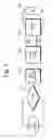
FIG. 1 is a schematic block diagram of an electronic ballast according to an embodiment of the present invention;
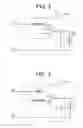
FIGS. 2 through 4 are circuit diagrams of resonant circuits of the electronic ballast of FIG. 1, according to embodiments of the present invention;
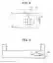
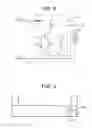
FIG. 5 is a front view of a fluorescent lamp case including a switch control according to an embodiment of the present invention;
FIG. 6 is a perspective view of the fluorescent lamp case of FIG. 5;
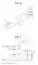
FIG. 7 is a circuit diagram of the resonant circuit of FIG. 3, according to another embodiment of the present invention;
FIG. 8 is a circuit diagram of the resonant circuit of FIG. 4, according to another embodiment of the present invention; and
FIG. 9 is a front view of a fluorescent lamp case including a switch control according to another embodiment of the present invention.
DETAILED DESCRIPTION OF THE INVENTION
The present invention will now be described more fully with reference to the accompanying drawings, in which exemplary embodiments of the invention are shown. In the drawings, the thicknesses of lines or the sizes of elements are exaggerated for clarity. Also, since later-described terms are defined in consideration of the functions of the present invention, they may vary according to users' intentions or practice. Hence, the terms must be interpreted based on the contents of the entire specification.
FIG. 1 is a schematic block diagram of an electronic ballast according to an embodiment of the present invention. Referring to FIG. 1, the electronic ballast includes a rectifier 10, a power factor compensator 20, an inverter 30, a resonant circuit 40, and a lamp 50.
An operation of the electronic ballast of the present embodiment will now be described in detail.
The rectifier 10 receives alternating current (AC) power from an external source and rectifies the AC power into direct current (DC) power. The power factor compensator 20 improves a power factor of the DC power. For example, the power factor compensator 20 improves the power factor of the DC power supplied from the rectifier 10 to about 99% using a semiconductor smoothing circuit used for compensating a power factor and considerably reduces a harmonic component of a current which is to be supplied to a system, in order to reduce noise caused by the rectification into the DC power.
The inverter 30 receives the DC power from the rectifier 10 and the power factor compensator 20, generates high frequency square wave power, and outputs the high frequency square wave power to the resonant circuit 40. The resonant circuit 40 receives the high frequency square wave power from the inverter 30, adjusts impedance using an inductor and a capacitor to adjust a resonant frequency, transforms the high frequency square wave power into high frequency sine wave power, and outputs the high frequency sine wave power. Here, power consumed by the lamp 50 is adjusted with the adjustment of the impedance. The lamp 50 emits light and varies illuminance according to the high frequency sine wave power supplied from the resonant circuit 40.
FIGS. 2 through 4 are circuit diagrams of the resonant circuit 40 of the electronic ballast of FIG. 1, according to embodiments of the present invention
As shown in FIGS. 2 and 3, the resonant circuit 40 includes a first resonant capacitor “C1,” a second resonant capacitor “C2,” and an inductance adjuster 210 or 310.
When a frequency of the high frequency square wave power output from the inverter 30 approaches a resonant frequency of the resonant circuit 40, the high frequency sine wave power is applied to the lamp 50. In other words, the resonant frequency of the resonant circuit 40 is adjusted with the adjustment of the inductor and the capacitor of the resonant circuit 40 and the high frequency square wave power is converted into the high frequency sine wave power. Thus, the consumed power of the lamp 50 is adjusted according to adjusted values of the inductor and the capacitor.
The resonant frequency is determined by values of the first resonant capacitor “C1,” the second resonance capacitor “C2,” and a variable inductor “L,” and an intensity of the variable inductor “L” may be adjusted by the inductance adjuster 210 according to an aspect of the present invention.
If the inverter 30 includes first and second nodes “N1” and “N2” as output nodes, an end of the first resonance capacitor “C1” is connected to the first node “N1,” and an other end of the first node “N1” is connected to the inductance adjuster 210. An end of the second resonant capacitor “C2” is connected to the second node “N2,” and an other end of the second resonant capacitor “C2” is connected to the inductance adjuster 210.
The inductance adjuster 210 includes the variable inductor “L” and a switch.
An end “S1” of the switch “S” is selectively connected to the variable inductor “L” of which other end is connected the other end of the first resonant capacitor “C1,” a node of the variable inductor “L,” or an other end of the variable inductor “L,” and an other end “S2” of the switch “S” is connected to the other end of the second resonant capacitor “C2.”
A value of the variable inductor “L” is adjusted depending on a switching operation selected by a user. Also, the user adjusts the resonant frequency of the resonant circuit 40 according to the value of the variable inductor “L” to generate the high frequency sine wave power which is output to the lamp 50 and simultaneously controls the consumed power of the lamp 50.
Referring to FIG. 3, an end of a first resonant inductor “L1” is connected to an end of a second resonant inductor “L2” in parallel and is connected to the first resonant capacitor “C1” in series, and other ends of the first and second resonant inductors “L1” and “L2” are connected to an end of the switch.
In other words, the end of the first resonant capacitor “C1” is connected to the first node “N1,” the other end of the first resonant capacitor “C1” is connected to the inductance adjuster 310, the end of the second resonant capacitor “C2” is connected to the second node “N2,” and the other end of the second resonant capacitor “C2” is connected to the inductance adjuster 310.
The inductance adjuster 310 includes the first resonant inductor “L1” of which end is connected to the other end of the first resonant capacitor “C1,” the second resonant inductor “L2,” of which end is connected to the other end of the first resonant capacitor “C1,” and the switch “S” of which end “S1” is selectively connected to an other end of the first resonant inductor “L1” or an other end of the second resonant inductor “L2,” and of which other end “S2” is connected to the other end of the second resonant capacitor “C2.”
A value of the first resonant inductor “L1” or the second resonant inductor “L2” is selected according to the switching operation selected by the user. Thus, the high frequency sine wave power output to the lamp 50 is controlled, and the consumed power of the lamp 50 is controlled.
The resonant circuit 40 includes one inductor “L” and one switch in FIG. 2 but two inductors and one switch in FIG. 3. However, it will be understood by those of ordinary skill in the art that the resonant circuit 40 may include a plurality of inductors and a plurality of switches.
This structure of the resonant circuit 40 will now be described with reference to FIG. 7.
Referring to FIG. 7, when the inverter 30 includes the first and second nodes “N1” and “N2” as output nodes, the resonant circuit 40 includes a first resonant capacitor “C1” of which end is connected to the first node “N1” and of which other end is connected to an inductance adjuster 610 and a second resonant capacitor “C2” of which end is connected to the second node “N2” and of which other end is connected to the inductance adjuster 610.
In particular, the inductance adjuster 610 includes first through nth inductors “L1,” “L2” . . . , and “Ln” having ends connected to an other end of the first resonant capacitor “C1” in parallel and a switch “S” of which ends “S1,” “S2,” . . . , and “Sn” are selectively connected to other ends of the first through nth inductors “L1,” “L2” . . . , and “Ln” and of which other end is connected to an other end of the second resonant capacitor “C2.”
The switch selects one of the other ends of the first through nth inductors “L1,” “L2” . . . , and “Ln” to vary an inductance value. Thus, the high frequency sine wave power output to the lamp 50 is controlled, and the consumed power of the lamp 50 is controlled.
Referring to FIG. 4, when the inverter 30 includes the first and second nodes “N1” and “N2” as output nodes, the resonant circuit 40 includes the first resonant capacitor “C1” and the inductor “L” which are sequentially connected to the first node “N1” in series and a capacitance adjuster 410 which is connected between the inductor “L” and the second node “N2.”
The capacitance adjuster 410 includes a second resonant capacitor “C21” of which end is connected to the second node “N2, a third resonant capacitor “C22” of which end is connected to the second node, and a switch of which end “S1” is selectively connected to an other end of the second resonant capacitor “C21” or an other end of the third resonant capacitor “C22” and of which other end “S2” is connected to the inductor “L.” The capacitance adjuster 410 includes two capacitors and one switch in FIG. 4 but may include a plurality of capacitors and a plurality of switches.
A value of the second resonant capacitor “C21” and the third resonant capacitance “C22” is selected depending on the switching operation selected by the user. Thus, the high frequency since wave power output to the lamp 50 is controlled, and the consumed power of the lamp 50 is controlled.
The structure of a capacitance adjuster including a plurality of capacitors and a plurality of switches will now be described with reference to FIG. 8. Referring to FIG. 8, a capacitance adjuster 710 includes second through nth resonant capacitors “C21,” “C22,” . . . , and “C2n” having ends connected to the second node “N2” in parall and a switch “S” of which ends “S1,” “S2,” . . . , and “Sn” are selectively connected to other ends of the second through nth resonant capacitors “C21,” “C22,” . . . , and “C2n” and of which other end is connected to the inductor “L.”
In the structure of the capacitance adjuster 710 of FIG. 8, one of the second through nth resonant capacitors “C21,” “C22,” . . . , and “C2n” is selectively selected to select various capacitance values. Thus, the high frequency sine wave power output to the lamp 50 is controlled, and the consumed power of the lamp 50 is controlled.
Here, the switch is connected to a switch control 510 which is positioned outside a fluorescent lamp case 500 so as to be controlled by the switch control 510. In other words, the switch control 510 controls the switches shown in FIGS. 2 through 4 to adjust capacitance and inductance so as to control the resonant frequency and the consumed power of the lamp 50. For example, when the switch control 510 is in a position “ON1,” the end “S1” of the switch is selected. When the switch control 510 is in a position “ON2,” the other end “S2” of the switch is selected. Thus, the capacitance and the inductance are controlled.
A switch control 910 of FIG. 9 may be used in the structures of the inductance adjuster 610 of FIG. 7 and the capacitance adjuster 710 8. In other words, since the inductance adjuster 610 of FIG. 7 includes the plurality of resonant inductors “L1,” “L2,” . . . , and “Ln” and the capacitance adjuster 710 of FIG. 8 includes the plurality of resonant capacitors “C21,” “C22,” . . . , and “C2n,” values of inductance and capacitance may be analogically controlled. Therefore, the user turns the switch control 910 of FIG. 9 on and/or off to adjust the values of the inductance and the capacitance so as to control the consumed power of the lamp 50.
Table 1 below shows consumed power, lamp output, and light speed with respect to values of inductance selected by the inductance adjusters 210 and 310.
| TABLE 1 | ||
| S1/L1 (7 mH) | S2/L2 (9 mH) |
| Sample 1 | Sample 2 | Sample 3 | Average | Sample 1 | Sample 2 | Sample 3 | Average | |
| Consumed | 30.78 | 30.80 | 30.80 | 30.79 | 25.98 | 26.33 | 26.17 | 26.16 |
| Power (W) | ||||||||
| Lamp Power | 27.98 | 28.00 | 28.00 | 27.99 | 23.62 | 23.94 | 23.79 | 23.78 |
| (W) | ||||||||
| Light Speed | 2451 | 2451 | 2507 | 2470 | 2137 | 2136 | 2126 | 2133 |
| (lm) | ||||||||
Here, a 28 W-high frequency (four high frequency (FHF)) lamp was used for sample 1, sample 2, and sample 3. According to the results of the experiment, when the 28 W-high frequency lamp is connected to the other end “S2” of the switch of FIG. 2 or an inductance value of the second resonant inductor “L2” of FIG. 3 is selected to 9 mH, the consumed power is more reduced by 4.6 W than when the 28 W-high frequency lamp is connected to the end “S1” of the switch of FIG. 2 or a inductance value of the first resonant inductor “L1” of FIG. 3 is selected to 7 mH. As a result, energy of about 15% is saved.
FIGS. 5 and 6 are a front view and a perspective view of the fluorescent lamp case 500 including the switch control 510 according to an embodiment of the present invention.
The user manipulates the switch control 510 of FIG. 5 or 6 to easily adjust an inductance or capacitance value of a resonant circuit.
For example, when the switch control 510 is in the position “ON1,” the end “S1” of the switch “S” is selected. When the switch control 510 is in the position “ON2,” the other end “S2 of the switch “S” is selected. As a result, the capacitance and inductance values are adjusted. In this case, energy is saved due to a reduction in consumed power as in the results of the experiment of Table 1 above.
As described above, an electronic ballast according to the present invention can vary an inductor or a capacitor of a resonant circuit according to a selection of a user to adjust consumed power of a lamp according to the selection of the user so as to save energy. Also, the user can further easily and conveniently control the consumed power through a switch control which is positioned outside a fluorescent lamp case.
While the present invention has been particularly shown and described with reference to exemplary embodiments thereof, it will be understood by those of ordinary skill in the art that various changes in form and details may be made therein without departing from the spirit and scope of the present invention as defined by the following claims.
Claims
1. An electronic ballast comprising:
a rectifier which rectifies alternating current (AC) power into direct current (DC) power;
a power factor compensator which improves a power face of the DC power;
an inverter which inverts the DC current into high frequency square wave power; and
a resonant circuit which receives the high frequency square wave power from the inverter, adjusts impedance, transforms the high frequency square wave power into high frequency sine wave power, and outputs the high frequency sine wave power.
2. The electronic ballast of claim 1, wherein the resonant circuit comprises an inductance adjuster and a capacitor.
3. The electronic ballast of claim 2, wherein when the inverter comprises first and second nodes as output nodes,
the resonant circuit comprises:
a first resonant capacitor which comprises an end connected to the first node and an other end connected to the inductance adjuster; and
a second resonant capacitor which comprises an end connected to the second node and an other end connected to the inductance adjuster, and
the inductance adjuster comprises:
a variable inductor which comprises an end connected to the another end of the first resonant capacitor; and
a switch which comprises an end selectively connected to one of a node and an other end of the variable inductor and an other end connected to the other end of the second resonant capacitor.
4. The electronic ballast of claim 2, wherein when the inverter comprises first and second nodes as output nodes,
the resonant circuit comprises:
a first resonant capacitor which comprises an end connected to the first node and an other end connected to the inductance adjuster; and
a second resonant capacitor which comprises an end connected to the second node and an other end connected to the inductance adjuster, and
the inductance adjuster comprises:
a first resonant inductor which comprises an end connected to the other end of the first resonant capacitor;
a second resonant inductor which comprises an end connected to an other end of the first resonant capacitor; and
a switch which comprises an end selectively connected to one of the other end of the first resonant inductor and an other end of the second resonant inductor and an other end connected to the other end of the second resonant capacitor.
5. The electronic ballast of claim 2, wherein when the inverter comprises first and second nodes as output nodes,
the resonant circuit comprises:
a first resonant capacitor which comprises an end connected to the first node and an other end connected to the inductance adjuster; and
a second resonant capacitor which comprises an end connected to the second node and an other end connected to the inductance adjuster, and
the inductance adjuster comprises:
first through nth resonant inductors which comprise ends respectively connected to the other end of the first resonant capacitor in parallel; and
a switch which comprises ends selectively connected to other ends of the first through nth resonant inductors and an other end connected to the other end of the second resonant capacitor.
6. The electronic ballast of claim 1, wherein when the inverter comprises first and second nodes as output nodes, the resonant circuit comprises a first resonant capacitor and an inductor which are sequentially connected to the first node and a capacitance adjuster which is connected between the inductor and the second node.
7. The electronic ballast of claim 6, wherein the capacitance adjuster comprises:
a second resonant capacitor which comprises an end connected to the second node;
a third resonant capacitor which comprises an end connected to the second node; and
a switch which comprises an end selectively connected to one of an other end of the second resonant capacitor and an other end of the third resonant capacitor and an other end connected to the inductor.
8. The electronic ballast of claim 6, wherein the capacitance adjuster comprises:
second through nth resonant capacitors which comprise ends respectively connected to the second node in parallel; and
a switch which comprises ends selectively connected to other ends of the second through nth resonant capacitors and an other end connected to the inductor.
9. The electronic ballast of claim 3, wherein the switch is connected to and controlled by a switch control which is positioned outside a fluorescent lamp case.
Images & Drawings included:

Sources:
- United States Patent and Trademark Office - verify current appl. status at the USPTO↗
Similar patent applications:
- » 20120235595
Method for Setting an Electronic Ballast, an Electronic Ballast and a Compensating Unit - » 20140001957
High intensity discharge electronic ballast circuit, electronic ballast, and high intensity discharge lamp - » 20120119652
Method of controlling an electronic ballast, an electronic ballast and a lighting controller - » 20160088713
Method for controlling time sharing starting of electronic ballasts and delayed-started electronic ballast - » 20120306408
Energy-recycling burn-in apparatus for electronic ballasts and a method of burning-in electronic ballasts - » 10179175
Electronic ballast and electronic transformer - » 20210410249
LED driving circuit compatible with electronic ballast and electronic supply, and LED lamp thereof - » 20050029966
Electronic ballast system having emergency lighting provisions and electronic chip - » 20140339996
BALLAST AND BALLAST CONTROL METHOD AND APPARATUS, FOR EXAMPLE ANTI-ARCING CONTROL FOR ELECTRONIC BALLAST - » 20100213866
Ballast and ballast control method and apparatus, for example anti-arcing control for electronic ballast
Recent applications in this class:
- » 20190029099 2019-01-24
LED LAMP - » 20120074871 2012-03-29
Apparatus for controlling power supplied to discharge lamp in response to command supplied from outside the apparatus - » 20120043898 2012-02-23
Electronic ballast and method for operation of at least one discharge lamp - » 20110273097 2011-11-10
Amp control system by controlling outputs of a buck DC-DC converter - » 20110096248 2011-04-28
Projector lamp lighting device supplying AC current including low frequency region having current reduction waveform - » 20110062885 2011-03-17
METHOD OF DRIVING AN UHP GAS-DISCHARGE LAMP - » 20100270939 2010-10-28
Method And Electronic Ballast for Operating a High Pressure Discharge Lamp - » 20100052561 2010-03-04
METHOD FOR DRIVING AN INVERTER OF A GAS DISCHARGE SUPPLY CIRCUIT - » 20090289572 2009-11-26
Ignition for ceramic metal halide high frequency ballasts - » 20090289566 2009-11-26
Lighting Device for a Discharge Lamp
Recent applications for this Assignee:
- » 20200240618 2020-07-30
Connection device and flexible lighting system with the same - » 20190350064 2019-11-14
Apparatus for generating PWM signal and apparatus for controlling light having the same - » 20190178480 2019-06-13
Lighting device - » 20160356470 2016-12-08
Lighting device - » 20150311689 2015-10-29
Wall structure and lighting system using the same - » 20140347036 2014-11-27
CURRENT MONITORING APPARATUS AND CURRENT MONITORING SYSTEM USING THE SAME - » 20140112001 2014-04-24
Lighting apparatus having rail unit - » 20120092875 2012-04-19
Lighting apparatus - » 20080278296 2008-11-13
Power line communication apparatus, and method and apparatus for controlling electric devices - » 20050125892 2005-06-16
Parabola type aqueduct