Multi-layer coating structure with anti-reflection, anti-static and anti-smudge functions and method for manufacturing the same
US20100173149A1
2010-07-08
12/318,670
2009-01-06
✅ Patent granted
US 8,173,202 B2
2012-05-08
-
-
James Lin
2030-10-28
Abstract:
A multi-layer coating structure with anti-reflection, anti-static and anti-smudge functions includes a substrate and a coating module. The coating module is formed on a front surface of the substrate and composed of a plurality of indium tin oxide compound coating layers and a plurality of silicon dioxide compound coating layers that are alternately stacked upon each other. The coating module further includes a fluorocarbon compound coating layer that is the uppermost layer of the coating module. Because the surface layer has good electrical conductive properties, the surface layer reduces much of the work in the grounding process and also increases the total yield and reliability in high volume production. The present invention provides a surface conductive layer structure with an anti-reflection coating that can be applied to the LCD and PDP display industries for glass and plastic film substrates.
Assignee:
- Innovation & Infinity Global Corp. 9 🇹🇼 Hsinchu, Taiwan
Interested in similar patents?
Get notified when new applications in this technology area are published.
Classification:
G02B1/111 » CPC main
Optical elements characterised by the material of which they are made; Optical coatings for optical elements; Optical coatings produced by application to, or surface treatment of, optical elements; Anti-reflection coatings using layers comprising organic materials
B05D5/083 » CPC further
Processes for applying liquids or other fluent materials to surfaces to obtain special surface effects, finishes or structures to obtain an anti-friction or anti-adhesive surface involving the use of fluoropolymers
C03C17/42 » CPC further
Surface treatment of glass, not in the form of fibres or filaments, by coating with at least two coatings having different compositions at least one coating of an organic material and at least one non-metal coating
G02B1/116 » CPC further
Optical elements characterised by the material of which they are made; Optical coatings for optical elements; Optical coatings produced by application to, or surface treatment of, optical elements; Anti-reflection coatings using inorganic layer materials only; Multilayers including electrically conducting layers
G02B1/16 » CPC further
Optical elements characterised by the material of which they are made; Optical coatings for optical elements; Optical coatings produced by application to, or surface treatment of, optical elements having an anti-static effect, e.g. electrically conducting coatings
G02B27/0006 » CPC further
Optical systems or apparatus not provided for by any of the groups - with means to keep optical surfaces clean, e.g. by preventing or removing dirt, stains, contamination, condensation
B05D2350/60 » CPC further
Pretreatment of the substrate Adding a layer before coating
C03C2217/734 » CPC further
Coatings on glass; Properties of coatings; Anti-reflective coatings with specific characteristics comprising an alternation of high and low refractive indexes
C03C2217/76 » CPC further
Coatings on glass; Properties of coatings Hydrophobic and oleophobic coatings
G02F1/133311 » CPC further
Devices or arrangements for the control of the intensity, colour, phase, polarisation or direction of light arriving from an independent light source, e.g. switching, gating or modulating; Non-linear optics for the control of the intensity, phase, polarisation or colour based on liquid crystals, e.g. single liquid crystal display cells; Constructional arrangements; Operation of liquid crystal cells; Circuit arrangements; Constructional arrangements; Manufacturing methods; Support structures for LCD panels, e.g. frames or bezels Environmental protection, e.g. against dust or humidity
G02F1/133502 » CPC further
Devices or arrangements for the control of the intensity, colour, phase, polarisation or direction of light arriving from an independent light source, e.g. switching, gating or modulating; Non-linear optics for the control of the intensity, phase, polarisation or colour based on liquid crystals, e.g. single liquid crystal display cells; Constructional arrangements; Operation of liquid crystal cells; Circuit arrangements; Constructional arrangements; Manufacturing methods; Structural association of cells with optical devices, e.g. polarisers or reflectors Antiglare, refractive index matching layers
G02F2202/22 » CPC further
Materials and properties Antistatic materials or arrangements
Y10T428/265 » CPC further
Stock material or miscellaneous articles; Web or sheet containing structurally defined element or component, the element or component having a specified physical dimension; Coating layer not in excess of 5 mils thick or equivalent; Up to 3 mils 1 mil or less
B32B17/06 IPC
Layered products essentially comprising sheet glass, or glass, slag, or like fibres comprising glass as the main or only constituent of a layer, next to another layer of a specific material
B32B9/04 IPC
Layered products comprising a layer of a particular substance not covered by groups - comprising such substance as the main or only constituent of a layer, next to another layer of a
B05D1/36 IPC
Processes for applying liquids or other fluent materials Successively applying liquids or other fluent materials, e.g. without intermediate treatment
B05D5/06 IPC
Processes for applying liquids or other fluent materials to surfaces to obtain special surface effects, finishes or structures to obtain multicolour or other optical effects
Description
BACKGROUND OF THE INVENTION
1. Field of the Invention
The present invention relates to a multi-layer coating structure and a method for manufacturing the same, and particularly relates to a multi-layer coating structure with anti-reflection, anti-static and anti-smudge functions and a method for manufacturing the same.
2. Description of Related Art
It is well known that the conventional layer structure for an anti-reflection optical coating has a general principle. This general principle is that the surface layer of the optical coating should be a material with low refractive index such as SiO2, with a refractive index of 1.46, or MgF2, with a refractive index of 1.38. However, when a metal based anti-reflection coating is applied on a display screen to create a high EMI shielding effect for a computer monitor, or low reflection glass for an LCD or a PDP, there are some bottlenecks in the process for high volume mass production. The basic reason for this is that the protective layer, for example SiO2 or MgF2, of the optical layer has a naturally porous microstructure and allows H2O vapor to diffuse into the thin, low resistivity metal layer, changing the electric and optical characteristics of the layer system. This optical layer structure has a high surface energy so that the optical layer structure absorbs dusts, pollutants or fingerprints easily.
SUMMARY OF THE INVENTION
One particular aspect of the present invention is to provide a multi-layer coating structure with anti-reflection, anti-static and anti-smudge functions. The process of manufacturing the multi-layer coating structure in high volume production is highly reliable and has been routinely used in industries such as semiconductor manufacturing, disc head manufacturing, LCD manufacturing, CRT manufacturing, architecture glass manufacturing, touch sensor display manufacturing, screen filter manufacturing and plastic web coating for more than twenty years.
The material of the surface layer of the present invention is a transparent conductive layer. The reflective index of the transparent surface conductive layer is below 0.5%. The resistivity of the anti-reflection coating is as low as 104 to 105 Ω-cm, and its transparency is between 90% and 95%.
In order to achieve the above-mentioned aspects, the present invention provides a multi-layer coating structure with anti-reflection, anti-static and anti-smudge functions, including: a substrate and a coating module. The coating module is formed on a front surface of the substrate and composed of a plurality of indium tin oxide compound coating layers and a plurality of silicon dioxide compound coating layers that are alternately stacked upon each other. The coating module further includes a fluorocarbon compound coating layer that is the uppermost layer of the coating module.
In order to achieve the above-mentioned aspects, the present invention provides a method for manufacturing a multi-layer coating structure with anti-reflection, anti-static and anti-smudge functions, including: providing a substrate; and then formed a coating module on a front surface of the substrate. The coating module is composed of a plurality of indium tin oxide compound coating layers and a plurality of silicon dioxide compound coating layers that are alternately stacked upon each other. The coating module further includes a fluorocarbon compound coating layer that is the uppermost layer of the coating module.
Because the surface layer has good electrical conductive properties, the surface layer reduces much of the work in the grounding process and also increases the total yield and reliability in high volume production. The present invention provides a surface conductive layer structure with an anti-reflection coating that can be applied to the LCD and PDP display industries for glass and plastic film substrates.
It is to be understood that both the foregoing general description and the following detailed description are exemplary, and are intended to provide further explanation of the invention as claimed. Other advantages and features of the invention will be apparent from the following description, drawings and claims.
BRIEF DESCRIPTION OF THE DRAWINGS
The various objects and advantages of the present invention will be more readily understood from the following detailed description when read in conjunction with the appended drawings, in which:
FIG. 1 is a front, schematic view of a multi-layer coating structure with anti-reflection, anti-static and anti-smudge functions according to the present invention;
FIG. 2 is a top, schematic view of a multi-layer coating structure with anti-reflection, anti-static and anti-smudge functions according to the present invention; and
FIG. 3 is a flow chart of a method for manufacturing a multi-layer coating structure with anti-reflection, anti-static and anti-smudge functions according to the present invention.
DETAILED DESCRIPTION OF PREFERRED EMBODIMENTS
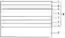
Referring to FIG. 1, the present invention provides a multi-layer coating structure with anti-reflection, anti-static and anti-smudge functions. The coating structure includes a substrate S and a coating module M.
The substrate S can be a plastic film or a glass. The coating module M can be a basic coating for a plasma display or a liquid crystal display.
Moreover, the coating module M includes a first coating layer 1 formed on a front surface of the substrate S, a second coating layer 2 formed on the first coating layer 1, a third coating layer 3 formed on the second coating layer 2, a fourth coating layer 4 formed on the third coating layer 3, a fifth coating layer 5 formed on the fourth coating layer 4, a sixth coating layer 6 formed on the fifth coating layer 5, and a seventh coating layer 7 formed on the sixth coating layer 6.
Furthermore the first coating layer 1, the third coating layer 3 and the fifth coating layer 5 are indium tin oxide compound coating layers. The second coating layer 2, the fourth coating layer 4 and the sixth coating layer 6 are silicon dioxide compound coating layers. In addition, each indium tin oxide compound coating layer is composed of 90% In2O3 and 10% SnO2 (In2O390% SnO210%), and each silicon dioxide compound coating layer is SiO2.
Therefore, the coating module M is formed on the front surface of the substrate S and is composed of a plurality of indium tin oxide compound coating layers and a plurality of silicon dioxide compound coating layers that are alternately stacked upon each other. The coating module M further includes a fluorocarbon compound coating layer that is the uppermost layer of the coating module M.
Moreover, the refractive indices of the first coating layer 1, the third coating layer 3 and the fifth coating layer 5 are 1.9˜2.0, and the refractive indices of the second coating layer 2, the fourth coating layer 4 and the sixth coating layer 6 are 1.4˜1.5. Furthermore, the thickness of the first coating layer 1 is 10˜20 nm, the thickness of the second coating layer 2 is 30˜50 nm, the thickness of the third coating layer 3 is 30˜50 nm, the thickness of the fourth coating layer 4 is 80˜100 nm, the thickness of the fifth coating layer 5 is 5˜10 nm, the thickness of the sixth coating layer 6 is 5˜10 nm, and the thickness of the seventh coating layer 7 is 5˜10 nm.
In addition, the first coating layer 1, the third coating layer 3 and the fifth coating layer 5 (the indium tin oxide compound coating layers) are formed by a DC or AC magnetron sputtering method. The second coating layer 2, the fourth coating layer 4 and the sixth coating layer 6 (the silicon dioxide compound coating layers) are formed by a DC or AC magnetron sputtering method. Moreover, all of the coating layers (from the first coating layer 1 to the sixth coating layer 6) are formed by an in-line or roll-to-roll vacuum sputtering method.
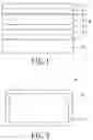
Referring to FIG. 2, the multi-layer coating structure of the present invention further includes a conductive layer C formed on a peripheral area of a top surface of the coating module M in order to connect to a ground. Therefore, the conductive layer C is formed on a peripheral area of a top surface of the seventh coating layer 7 of the coating module M for connecting to the ground. In other words, after the coating module M is formed on the substrate S, a shutter B is placed on the top surface of the coating module M. The shutter B has a size smaller than that of the coating module M in order to expose a peripheral area of the top surface of the coating module M. Afterward a conductive layer C is coated on the peripheral area of the top surface of the coating module M in order to connect to the ground and achieve good electrical contact. Finally, the shutter B is removed. In addition, the conductive layer C can be a silver paste.
Referring to FIG. 3, the present invention provides a method for manufacturing a multi-layer coating structure with anti-reflection, anti-static and anti-smudge functions. The method includes:
S100: a substrate S is provided;
S102: a first coating layer 1 is formed on a front surface of the substrate S, and the first coating layer 1 is the indium tin oxide compound coating layer;
S104: a second coating layer 2 is formed on the first coating layer 1, and the second coating layer 2 is the silicon dioxide compound coating layer;
S106: a third coating layer 3 is formed on the second coating layer 2, and the third coating layer 3 is the indium tin oxide compound coating layer;
S108: a fourth coating layer 4 is formed on the third coating layer 3, and the fourth coating layer 4 is the silicon dioxide compound coating layer;
S110: a fifth coating layer 5 is formed on the fourth coating layer 4, and the fifth coating layer 5 is the indium tin oxide compound coating layer;
S112: a sixth coating layer 6 is formed on the fifth coating layer 5, and the sixth coating layer 6 is the silicon dioxide compound coating layer; and
S114: a seventh coating layer 7 is formed on the sixth coating layer 6, and the seventh coating layer 7 is the fluorocarbon compound coating layer.
In one embodiment the present invention of the anti-reflection coating structure has 7 layers and includes a first coating layer, a second coating layer, a third coating layer, a fourth coating layer, a fifth coating layer, a sixth coating layer and a seventh coating layer formed on a substrate in sequence. Each layer is described in terms of physical or optical thickness. The optical thickness is the mathematical product of a layer's thickness and its refractive index. It is described as a fraction of a designed wavelength. In the present invention the designed wavelength is about 520 nm.
The first coating layer or the surface layer is an indium tin oxide compound coating layer with a refractive index between 1.9 and 2.0 and a physical thickness of 30˜50 nm.
The second coating layer is a silicon dioxide compound coating layer with a refractive index between 1.4 and 1.5 and a physical thickness of 10 to 18 nm.
The third coating layer is an indium tin oxide compound coating layer with a refractive index between 1.9 and 2.0 and a physical thickness of 30˜50 nm.
The fourth coating layer is a silicon dioxide compound coating layer with a refractive index between 1.4 and 1.5 and a physical thickness of 80 to 100 nm.
The fifth coating layer is an indium tin oxide compound coating layer with a refractive index between 1.9 and 2.0 and a physical thickness of 5˜10 nm.
The sixth coating layer is a silicon dioxide compound coating layer with a refractive index between 1.4 and 1.5 and a physical thickness of 5 to 10 nm.
The sixth coating layer is a fluorocarbon compound coating layer with a refractive index between 1.4 and 1.5 and a physical thickness of 5 to 10 nm.
In conclusion, the process of manufacturing the multi-layer coating structure in high volume production is highly reliable and has been routinely used in industries such as semiconductor manufacturing, disc head manufacturing, LCD manufacturing, CRT manufacturing, architecture glass manufacturing, touch sensor display manufacturing, screen filter manufacturing and plastic web coating for more than twenty years. The material of the surface layer of the present invention is a transparent conductive layer. The reflective index of the transparent surface conductive layer is below 0.5%. The resistivity of the anti-reflection coating is as low as 104 to 105 Ω-cm, and its transparency is between 90% and 95%.
Because the surface layer has good electrical conductive properties, the surface layer reduces much of the work in the grounding process and also increases the total yield and reliability in high volume production. The present invention provides a surface conductive layer structure with an anti-reflection coating that can be applied to the LCD and PDP display industries for glass and plastic film substrates.
Although the present invention has been described with reference to the preferred best molds thereof, it will be understood that the present invention is not limited to the details thereof. Various substitutions and modifications have been suggested in the foregoing description, and others will occur to those of ordinary skill in the art. Therefore, all such substitutions and modifications are intended to be embraced within the scope of the invention as defined in the appended claims.
Claims
What is claimed is:1. A multi-layer coating structure with anti-reflection, anti-static and anti-smudge functions, comprising:
a substrate; and
a coating module formed on a front surface of the substrate and composed of a plurality of indium tin oxide compound coating layers and a plurality of silicon dioxide compound coating layers that are alternately stacked upon each other, wherein the coating module further comprises a fluorocarbon compound coating layer that is the uppermost layer of the coating module.
2. The multi-layer coating structure as claimed in claim 1, wherein the substrate is a plastic film.
3. The multi-layer coating structure as claimed in claim 1, wherein the substrate is a glass.
4. The multi-layer coating structure as claimed in claim 1, wherein the coating module is a basic coating for a plasma display or a liquid crystal display.
5. The multi-layer coating structure as claimed in claim 1, wherein the coating module comprises:
a first coating layer formed on the front surface of the substrate;
a second coating layer formed on the first coating layer;
a third coating layer formed on the second coating layer;
a fourth coating layer formed on the third coating layer;
a fifth coating layer formed on the fourth coating layer;
a sixth coating layer formed on the fifth coating layer; and
a seventh coating layer formed on the sixth coating layer;
wherein the first coating layer, the third coating layer and the fifth coating layer are the indium tin oxide compound coating layers; wherein the second coating layer, the fourth coating layer and the sixth coating layer are the silicon dioxide compound coating layers; wherein the seventh coating layer is the fluorocarbon compound coating layer.
6. The multi-layer coating structure as claimed in claim 5, wherein each indium tin oxide compound coating layer is composed of 90% In2O3 and 10% SnO2 (In2O390% SnO210%), and each silicon dioxide compound coating layer is SiO2.
7. The multi-layer coating structure as claimed in claim 5, wherein the refractive indices of the first coating layer, the third coating layer, the fifth coating layer and the seventh coating layer are 1.9˜2.0, and the refractive indices of the second coating layer, the fourth coating layer and the sixth coating layer are 1.4˜1.5.
8. The multi-layer coating structure as claimed in claim 5, wherein the first coating layer has a thickness of 10˜20 nm; the second coating layer has a thickness of 30˜50 nm; the third coating layer has a thickness of 30˜50 nm; the fourth coating layer has a thickness of 80˜100 nm; the fifth coating layer has a thickness of 5˜10 nm; the sixth coating layer has a thickness of 5˜10 nm; the seventh coating layer has a thickness of 5˜10 nm.
9. The multi-layer coating structure as claimed in claim 1, further comprising a conductive layer formed on a peripheral area of a top surface of the coating module in order to connect to a ground.
10. A method for manufacturing a multi-layer coating structure with anti-reflection, anti-static and anti-smudge functions, comprising:
providing a substrate; and
formed a coating module on a front surface of the substrate, wherein the coating module is composed of a plurality of indium tin oxide compound coating layers and a plurality of silicon dioxide compound coating layers that are alternately stacked upon each other, wherein the coating module further comprises a fluorocarbon compound coating layer that is the uppermost layer of the coating module.
11. The method as claimed in claim 10, wherein the substrate is a plastic film.
12. The method as claimed in claim 10, wherein the substrate is a glass.
13. The method as claimed in claim 10, wherein the coating module is a basic coating for a plasma display or a liquid crystal display.
14. The method as claimed in claim 10, wherein the coating module comprises:
forming a first coating layer on the front surface of the substrate, wherein the first coating layer is the indium tin oxide compound coating layer;
forming a second coating layer on the first coating layer, wherein the second coating layer is the silicon dioxide compound coating layer;
forming a third coating layer on the second coating layer, wherein the third coating layer is the indium tin oxide compound coating layer;
forming a fourth coating layer on the third coating layer, wherein the fourth coating layer is the silicon dioxide compound coating layer;
forming a fifth coating layer on the fourth coating layer, wherein the fifth coating layer is the indium tin oxide compound coating layer;
forming a sixth coating layer on the fifth coating layer, wherein the sixth coating layer is the silicon dioxide compound coating layer; and
forming a seventh coating layer on the sixth coating layer, wherein the seventh coating layer is the fluorocarbon compound coating layer.
15. The method as claimed in claim 14, wherein each indium tin oxide compound coating layer is composed of 90% In2O3 and 10% SnO2 (In2O390% SnO210%), and each silicon dioxide compound coating layer is SiO2.
16. The method as claimed in claim 14, wherein the refractive indices of the first coating layer, the third coating layer and the fifth coating layer are 1.9˜2.0, and the refractive indices of the second coating layer, the fourth coating layer and the sixth coating layer are 1.4˜1.5.
17. The method as claimed in claim 14, wherein the first coating layer has a thickness of 10˜20 nm; the second coating layer has a thickness of 30˜50 nm; the third coating layer has a thickness of 30˜50 nm; the fourth coating layer has a thickness of 80˜100 nm; the fifth coating layer has a thickness of 5˜10 nm; the sixth coating layer has a thickness of 5˜10 nm; the seventh coating layer has a thickness of 5˜10 nm.
18. The method as claimed in claim 10, further comprising:
placing a shutter on a top surface of the coating module, wherein the shutter has a size smaller than that of the coating module for exposing a peripheral area of the top surface of the coating module; and
coating a conductive layer on the peripheral area of the top surface of the coating module in order to connect to a ground.
Images & Drawings included:

Sources:
- United States Patent and Trademark Office - verify current appl. status at the USPTO↗
Recent applications in this class:
- » 20250284033 2025-09-11
LENS AND MANUFACTURING METHOD THEREOF - » 20250264639 2025-08-21
OPTICAL FILM, IMAGE DISPLAY PANEL, AND IMAGE DISPLAY DEVICE - » 20250258320 2025-08-14
ANTIREFLECTION COATING MATERIAL, OPTICAL MEMBER WITH ANTIREFLECTION COATING, OPTICAL DEVICE, AND IMAGE CAPTURING APPARATUS - » 20250189696 2025-06-12
ANTIREFLECTIVE MEMBER, AND POLARIZING PLATE, IMAGE DISPLAY DEVICE AND ANTIREFLECTIVE ARTICLE EACH EQUIPPED WITH SAME - » 20250155606 2025-05-15
ANTIREFLECTIVE MEMBER, AND POLARIZING PLATE, IMAGE DISPLAY PANEL, IMAGE DISPLAY DEVICE, AND ANTIREFLECTIVE ARTICLE WHICH USE SAID ANTIREFLECTIVE MEMBER, AND METHOD FOR SELECTING ANTIREFLECTIVE MEMBER - » 20250123423 2025-04-17
UV-BLOCKING FILM FOR ARCHITECTURAL AND AUTOMOTIVE WITH 100% UV AND BLUE LIGHT BLOCKING - » 20250110261 2025-04-03
Optical Film and Optical Lens Including Same - » 20250102706 2025-03-27
ANTI-GLARE LAYERS AND DISPLAY PANELS - » 20250076540 2025-03-06
LAMINATED BODY, OPTICAL DEVICE, IMAGING APPARATUS, AND DISPLAY APPARATUS - » 20250067904 2025-02-27
ANTI-REFLECTIVE MULTI-LAYER SYSTEMS
Recent applications for this Assignee:
- » 20130278508 2013-10-24
Touch sensing device and touch sensing method thereof - » 20120279759 2012-11-08
Transparent conductive structure applied to a touch panel and method of making the same - » 20100233388 2010-09-16
Multilayer film structure for increasing transmittance and method for manufacturing the same - » 20090297878 2009-12-03
Extreme low resistivity light attenuation anti-reflection coating structure in order to increase transmittance of blue light and method for manufacturing the same - » 20090297877 2009-12-03
Extreme low resistivity light attenuation anti-reflection coating structure in order to increase transmittance of blue light and method for manufacturing the same - » 20090092850 2009-04-09
Extreme low resistivity light attenuation anti-reflection coating structure and method for manufacturing the same - » 20090092825 2009-04-09
Extreme low resistivity light attenuation anti-reflection coating structure and method for manufacturing the same - » 20080248219 2008-10-09
Anti-reflection coating with low resistivity function and transparent conductive coating as outermost layer