Fluid-ejecting integrated circuit utilizing electromagnetic displacement
US20100182379A1
2010-07-22
12/750,578
2010-03-30
✅ Patent granted
US 7,988,262 B2
2011-08-02
-
-
Lam S Nguyen
2030-03-30
Abstract:
A fluid ejecting integrated circuit (IC) includes a nozzle chamber defined by chamber side walls extending from a wafer substrate, and a roof wall provided on the chamber side walls; a fluid ejecting member provided within the nozzle chamber between the roof wall of the nozzle chamber and the wafer substrate; a support formation provided within the nozzle chamber and spaced inwardly away from the chamber side walls, the support formation extending from the wafer substrate to support the fluid ejecting member thereon; a first planar electrode layered to the fluid ejecting member; a second planar electrode layered on the wafer substrate; and a projection provided on the first planar electrode on a side facing the second planar electrode, the projection for contacting the second planar electrode to prevent contact between the first planar electrode and the second planar electrode. The first and second planar electrode establish a potential therebetween to deform the first planar electrode towards the second planar electrode.
Assignee:
- Silverbrook Research Pty Ltd 3,043 🇦🇺 Balmain, New South Wales, Australia
Interested in similar patents?
Get notified when new applications in this technology area are published.
Classification:
H04N5/2628 » CPC main
Details of television systems; Studio circuitry; Studio devices; Studio equipment ; Cameras comprising an electronic image sensor, e.g. digital cameras, video cameras, TV cameras, video cameras, camcorders, webcams, camera modules for embedding in other devices, e.g. mobile phones, computers or vehicles; Studio circuits, e.g. for mixing, switching-over, change of character of image, other special effects ; Cameras specially adapted for the electronic generation of special effects Alteration of picture size, shape, position or orientation, e.g. zooming, rotation, rolling, perspective, translation
B41J2/14 » CPC further
Typewriters or selective printing mechanisms characterised by the printing or marking process for which they are designed characterised by bringing liquid or particles selectively into contact with a printing material; Ink jet; Nozzles Structure thereof only for on-demand ink jet heads
B41J2/14314 » CPC further
Typewriters or selective printing mechanisms characterised by the printing or marking process for which they are designed characterised by bringing liquid or particles selectively into contact with a printing material; Ink jet; Nozzles; Structure thereof only for on-demand ink jet heads Structure of ink jet print heads with electrostatically actuated membrane
B41J2/16 » CPC further
Typewriters or selective printing mechanisms characterised by the printing or marking process for which they are designed characterised by bringing liquid or particles selectively into contact with a printing material; Ink jet; Nozzles Production of nozzles
B41J2/1623 » CPC further
Typewriters or selective printing mechanisms characterised by the printing or marking process for which they are designed characterised by bringing liquid or particles selectively into contact with a printing material; Ink jet; Nozzles; Production of nozzles manufacturing processes bonding and adhesion
B41J2/1626 » CPC further
Typewriters or selective printing mechanisms characterised by the printing or marking process for which they are designed characterised by bringing liquid or particles selectively into contact with a printing material; Ink jet; Nozzles; Production of nozzles manufacturing processes etching
B41J2/1631 » CPC further
Typewriters or selective printing mechanisms characterised by the printing or marking process for which they are designed characterised by bringing liquid or particles selectively into contact with a printing material; Ink jet; Nozzles; Production of nozzles manufacturing processes photolithography
B41J2/1632 » CPC further
Typewriters or selective printing mechanisms characterised by the printing or marking process for which they are designed characterised by bringing liquid or particles selectively into contact with a printing material; Ink jet; Nozzles; Production of nozzles manufacturing processes machining
B41J2/1635 » CPC further
Typewriters or selective printing mechanisms characterised by the printing or marking process for which they are designed characterised by bringing liquid or particles selectively into contact with a printing material; Ink jet; Nozzles; Production of nozzles manufacturing processes dividing the wafer into individual chips
B41J2/1637 » CPC further
Typewriters or selective printing mechanisms characterised by the printing or marking process for which they are designed characterised by bringing liquid or particles selectively into contact with a printing material; Ink jet; Nozzles; Production of nozzles manufacturing processes molding
B41J2/17503 » CPC further
Typewriters or selective printing mechanisms characterised by the printing or marking process for which they are designed characterised by bringing liquid or particles selectively into contact with a printing material; Ink jet characterised by ink handling; Ink supply systems ; Circuit parts therefor Ink cartridges
B41J2/17513 » CPC further
Typewriters or selective printing mechanisms characterised by the printing or marking process for which they are designed characterised by bringing liquid or particles selectively into contact with a printing material; Ink jet characterised by ink handling; Ink supply systems ; Circuit parts therefor; Ink cartridges Inner structure
G06F21/79 » CPC further
Security arrangements for protecting computers, components thereof, programs or data against unauthorised activity; Protecting specific internal or peripheral components, in which the protection of a component leads to protection of the entire computer to assure secure storage of data in semiconductor storage media, e.g. directly-addressable memories
G06F21/86 » CPC further
Security arrangements for protecting computers, components thereof, programs or data against unauthorised activity; Protecting specific internal or peripheral components, in which the protection of a component leads to protection of the entire computer Secure or tamper-resistant housings
G06K1/121 » CPC further
Methods or arrangements for marking the record carrier in digital fashion otherwise than by punching by printing code marks
G06K7/14 » CPC further
Methods or arrangements for sensing record carriers, e.g. for reading patterns by electromagnetic radiation, e.g. optical sensing; by corpuscular radiation using light without selection of wavelength, e.g. sensing reflected white light
G06K7/1417 » CPC further
Methods or arrangements for sensing record carriers, e.g. for reading patterns by electromagnetic radiation, e.g. optical sensing; by corpuscular radiation using light without selection of wavelength, e.g. sensing reflected white light; Methods for optical code recognition the method being specifically adapted for the type of code 2D bar codes
G06K19/06037 » CPC further
Record carriers for use with machines and with at least a part designed to carry digital markings characterised by the kind of the digital marking, e.g. shape, nature, code with optically detectable marking multi-dimensional coding
G06K19/073 » CPC further
Record carriers for use with machines and with at least a part designed to carry digital markings characterised by the kind of the digital marking, e.g. shape, nature, code; Record carriers with conductive marks, printed circuits or semiconductor circuit elements, e.g. credit or identity cards also with resonating or responding marks without active components with integrated circuit chips Special arrangements for circuits, e.g. for protecting identification code in memory
G11C11/56 » CPC further
Digital stores characterised by the use of particular electric or magnetic storage elements; Storage elements therefor using storage elements with more than two stable states represented by steps, e.g. of voltage, current, phase, frequency
H04N1/2112 » CPC further
Scanning, transmission or reproduction of documents or the like, e.g. facsimile transmission; Details thereof; Intermediate information storage for one or a few pictures using still video cameras
H04N1/2154 » CPC further
Scanning, transmission or reproduction of documents or the like, e.g. facsimile transmission; Details thereof; Intermediate information storage for one or a few pictures using still video cameras the still video camera incorporating a hardcopy reproducing device, e.g. a printer
H04N5/225 » CPC further
Details of television systems; Studio circuitry; Studio devices; Studio equipment ; Cameras comprising an electronic image sensor, e.g. digital cameras, video cameras, TV cameras, video cameras, camcorders, webcams, camera modules for embedding in other devices, e.g. mobile phones, computers or vehicles Television cameras ; Cameras comprising an electronic image sensor, e.g. digital cameras, video cameras, camcorders, webcams, camera modules specially adapted for being embedded in other devices, e.g. mobile phones, computers or vehicles
B41J2/16585 » CPC further
Typewriters or selective printing mechanisms characterised by the printing or marking process for which they are designed characterised by bringing liquid or particles selectively into contact with a printing material; Ink jet; Nozzles; Preventing or detecting of nozzle clogging, e.g. cleaning, capping or moistening for nozzles for paper-width or non-reciprocating print heads
B41J2/17596 » CPC further
Typewriters or selective printing mechanisms characterised by the printing or marking process for which they are designed characterised by bringing liquid or particles selectively into contact with a printing material; Ink jet characterised by ink handling; Ink supply systems ; Circuit parts therefor Ink pumps, ink valves
B41J2002/041 » CPC further
Typewriters or selective printing mechanisms characterised by the printing or marking process for which they are designed characterised by bringing liquid or particles selectively into contact with a printing material; Ink jet characterised by the jet generation process generating single droplets or particles on demand Electromagnetic transducer
B41J2202/21 » CPC further
Embodiments of or processes related to ink-jet or thermal heads; Embodiments of or processes related to ink-jet heads Line printing
G06F2221/2129 » CPC further
Indexing scheme relating to security arrangements for protecting computers, components thereof, programs or data against unauthorised activity; Indexing scheme relating to and subgroups addressing additional information or applications relating to security arrangements for protecting computers, components thereof, programs or data against unauthorised activity Authenticate client device independently of the user
H04N2101/00 » CPC further
Still video cameras
B41J2/04 » CPC further
Typewriters or selective printing mechanisms characterised by the printing or marking process for which they are designed characterised by bringing liquid or particles selectively into contact with a printing material; Ink jet characterised by the jet generation process generating single droplets or particles on demand
B41J2/045 IPC
Typewriters or selective printing mechanisms characterised by the printing or marking process for which they are designed characterised by bringing liquid or particles selectively into contact with a printing material; Ink jet characterised by the jet generation process generating single droplets or particles on demand by pressure, e.g. electromechanical transducers
Description
CROSS REFERENCE TO RELATED APPLICATION
The present application is a continuation of U.S. application Ser. No. 11/583,826 filed on Oct. 20, 2006, which is a continuation of U.S. application Ser. No. 10/957,718 filed on Oct. 5, 2004, now issued as U.S. Pat. No. 7,140,723, which is a continuation of U.S. application Ser. No. 10/184,883 filed on Jul. 1, 2002, now issued as U.S. Pat. No. 6,820,968, which is a continuation of U.S. application Ser. No. 09/113,070 filed Jul. 10, 1998, now issued as U.S. Pat. No. 6,476,863, the entire contents of which are herein incorporated by reference.
The following Australian provisional patent applications are hereby incorporated by cross-reference. For the purposes of location and identification, US patent applications identified by their US patent application serial numbers (USSN) are listed alongside the Australian applications from which the U.S. patent applications claim the right of priority.
| US Patent Application | |||
| Cross-Referenced | (Claiming Right | ||
| Australian | of Priority from | ||
| Provisional | Australian Provisional | ||
| Patent No. | Application) | Docket No. | |
| PO7991 | 6,750,901 | ART01US | |
| PO8505 | 6,476,863 | ART02US | |
| PO7988 | 6,788,336 | ART03US | |
| PO9395 | 6,322,181 | ART04US | |
| PO8017 | 6,597,817 | ART06US | |
| PO8014 | 6,227,648 | ART07US | |
| PO8025 | 6,727,948 | ART08US | |
| PO8032 | 6,690,419 | ART09US | |
| PO7999 | 6,727,951 | ART10US | |
| PO8030 | 6,196,541 | ART13US | |
| PO7997 | 6,195,150 | ART15US | |
| PO7979 | 6,362,868 | ART16US | |
| PO7978 | 6,831,681 | ART18US | |
| PO7982 | 6,431,669 | ART19US | |
| PO7989 | 6,362,869 | ART20US | |
| PO8019 | 6,472,052 | ART21US | |
| PO7980 | 6,356,715 | ART22US | |
| PO8018 | 6,894,694 | ART24US | |
| PO7938 | 6,636,216 | ART25US | |
| PO8016 | 6,366,693 | ART26US | |
| PO8024 | 6,329,990 | ART27US | |
| PO7939 | 6,459,495 | ART29US | |
| PO8501 | 6,137,500 | ART30US | |
| PO8500 | 6,690,416 | ART31US | |
| PO7987 | 7,050,143 | ART32US | |
| PO8022 | 6,398,328 | ART33US | |
| PO8497 | 7,110,024 | ART34US | |
| PO8020 | 6,431,704 | ART38US | |
| PO8504 | 6,879,341 | ART42US | |
| PO8000 | 6,415,054 | ART43US | |
| PO7934 | 6,665,454 | ART45US | |
| PO7990 | 6,542,645 | ART46US | |
| PO8499 | 6,486,886 | ART47US | |
| PO8502 | 6,381,361 | ART48US | |
| PO7981 | 6,317,192 | ART50US | |
| PO7986 | 6,850,274 | ART51US | |
| PO8026 | 6,646,757 | ART53US | |
| PO8028 | 6,624,848 | ART56US | |
| PO9394 | 6,357,135 | ART57US | |
| PO9397 | 6,271,931 | ART59US | |
| PO9398 | 6,353,772 | ART60US | |
| PO9399 | 6,106,147 | ART61US | |
| PO9400 | 6,665,008 | ART62US | |
| PO9401 | 6,304,291 | ART63US | |
| PO9403 | 6,305,770 | ART65US | |
| PO9405 | 6,289,262 | ART66US | |
| PP0959 | 6,315,200 | ART68US | |
| PP1397 | 6,217,165 | ART69US | |
| PP2370 | 6,786,420 | DOT01US | |
| PO8003 | 6,350,023 | Fluid01US | |
| PO8005 | 6,318,849 | Fluid02US | |
| PO8066 | 6,227,652 | IJ01US | |
| PO8072 | 6,213,588 | IJ02US | |
| PO8040 | 6,213,589 | IJ03US | |
| PO8071 | 6,231,163 | IJ04US | |
| PO8047 | 6,247,795 | IJ05US | |
| PO8035 | 6,394,581 | IJ06US | |
| PO8044 | 6,244,691 | IJ07US | |
| PO8063 | 6,257,704 | IJ08US | |
| PO8057 | 6,416,168 | IJ09US | |
| PO8056 | 6,220,694 | IJ10US | |
| PO8069 | 6,257,705 | IJ11US | |
| PO8049 | 6,247,794 | IJ12US | |
| PO8036 | 6,234,610 | IJ13US | |
| PO8048 | 6,247,793 | IJ14US | |
| PO8070 | 6,264,306 | IJ15US | |
| PO8067 | 6,241,342 | IJ16US | |
| PO8001 | 6,247,792 | IJ17US | |
| PO8038 | 6,264,307 | IJ18US | |
| PO8033 | 6,254,220 | IJ19US | |
| PO8002 | 6,234,611 | IJ20US | |
| PO8068 | 6,302,528 | IJ21US | |
| PO8062 | 6,283,582 | IJ22US | |
| PO8034 | 6,239,821 | IJ23US | |
| PO8039 | 6,338,547 | IJ24US | |
| PO8041 | 6,247,796 | IJ25US | |
| PO8004 | 6,557,977 | IJ26US | |
| PO8037 | 6,390,603 | IJ27US | |
| PO8043 | 6,362,843 | IJ28US | |
| PO8042 | 6,293,653 | IJ29US | |
| PO8064 | 6,312,107 | IJ30US | |
| PO9389 | 6,227,653 | IJ31US | |
| PO9391 | 6,234,609 | IJ32US | |
| PP0888 | 6,238,040 | IJ33US | |
| PP0891 | 6,188,415 | IJ34US | |
| PP0890 | 6,227,654 | IJ35US | |
| PP0873 | 6,209,989 | IJ36US | |
| PP0993 | 6,247,791 | IJ37US | |
| PP0890 | 6,336,710 | IJ38US | |
| PP1398 | 6,217,153 | IJ39US | |
| PP2592 | 6,416,167 | IJ40US | |
| PP2593 | 6,243,113 | IJ41US | |
| PP3991 | 6,283,581 | IJ42US | |
| PP3987 | 6,247,790 | IJ43US | |
| PP3985 | 6,260,953 | IJ44US | |
| PP3983 | 6,267,469 | IJ45US | |
| PO7935 | 6,224,780 | IJM01US | |
| PO7936 | 6,235,212 | IJM02US | |
| PO7937 | 6,280,643 | IJM03US | |
| PO8061 | 6,284,147 | IJM04US | |
| PO8054 | 6,214,244 | IJM05US | |
| PO8065 | 6,071,750 | IJM06US | |
| PO8055 | 6,267,905 | IJM07US | |
| PO8053 | 6,251,298 | IJM08US | |
| PO8078 | 6,258,285 | IJM09US | |
| PO7933 | 6,225,138 | IJM10US | |
| PO7950 | 6,241,904 | IJM11US | |
| PO7949 | 6,299,786 | IJM12US | |
| PO8060 | 6,866,789 | IJM13US | |
| PO8059 | 6,231,773 | IJM14US | |
| PO8073 | 6,190,931 | IJM15US | |
| PO8076 | 6,248,249 | IJM16US | |
| PO8075 | 6,290,862 | IJM17US | |
| PO8079 | 6,241,906 | IJM18US | |
| PO8050 | 6,565,762 | IJM19US | |
| PO8052 | 6,241,905 | IJM20US | |
| PO7948 | 6,451,216 | IJM21US | |
| PO7951 | 6,231,772 | IJM22US | |
| PO8074 | 6,274,056 | IJM23US | |
| PO7941 | 6,290,861 | IJM24US | |
| PO8077 | 6,248,248 | IJM25US | |
| PO8058 | 6,306,671 | IJM26US | |
| PO8051 | 6,331,258 | IJM27US | |
| PO8045 | 6,110,754 | IJM28US | |
| PO7952 | 6,294,101 | IJM29US | |
| PO8046 | 6,416,679 | IJM30US | |
| PO9390 | 6,264,849 | IJM31US | |
| PO9392 | 6,254,793 | IJM32US | |
| PP0889 | 6,235,211 | IJM35US | |
| PP0887 | 6,491,833 | IJM36US | |
| PP0882 | 6,264,850 | IJM37US | |
| PP0874 | 6,258,284 | IJM38US | |
| PP1396 | 6,312,615 | IJM39US | |
| PP3989 | 6,228,668 | IJM40US | |
| PP2591 | 6,180,427 | IJM41US | |
| PP3990 | 6,171,875 | IJM42US | |
| PP3986 | 6,267,904 | IJM43US | |
| PP3984 | 6,245,247 | IJM44US | |
| PP3982 | 6,315,914 | IJM45US | |
| PP0895 | 6,231,148 | IR01US | |
| PP0869 | 6,293,658 | IR04US | |
| PP0887 | 6,614,560 | IR05US | |
| PP0885 | 6,238,033 | IR06US | |
| PP0884 | 6,312,070 | IR10US | |
| PP0886 | 6,238,111 | IR12US | |
| PP0877 | 6,378,970 | IR16US | |
| PP0878 | 6,196,739 | IR17US | |
| PP0883 | 6,270,182 | IR19US | |
| PP0880 | 6,152,619 | IR20US | |
| PO8006 | 6,087,638 | MEMS02US | |
| PO8007 | 6,340,222 | MEMS03US | |
| PO8010 | 6,041,600 | MEMS05US | |
| PO8011 | 6,299,300 | MEMS06US | |
| PO7947 | 6,067,797 | MEMS07US | |
| PO7944 | 6,286,935 | MEMS09US | |
| PO7946 | 6,044,646 | MEMS10US | |
| PP0894 | 6,382,769 | MEMS13US | |
FIELD OF THE INVENTION
The present invention relates to fluid dispensing. In particular, this invention discloses a micro-electromechanical fluid-dispensing device.
BACKGROUND OF THE INVENTION
This invention is a development of a printing technology that has been developed by the Applicant. This development can be traced by considering the referenced patents/patent applications set out above.
Many different types of printing have been invented, a large number of which are presently in use. The known forms of printing have a variety of methods for marking the print media with a relevant marking media. Commonly used forms of printing include offset printing, laser printing and copying devices, dot matrix type impact printers, thermal paper printers, film recorders, thermal wax printers, dye sublimation printers and ink jet printers both of the drop on demand and continuous flow type. Each type of printer has its own advantages and problems when considering cost, speed, quality, reliability, simplicity of construction and operation etc.
In recent years, the field of ink jet printing, wherein each individual pixel of ink is derived from one or more ink nozzles has become increasingly popular primarily due to its inexpensive and versatile nature.
Many different techniques of ink jet printing have been invented. For a survey of the field, reference is made to an article by J Moore, “Non-Impact Printing: Introduction and Historical Perspective”, Output Hard Copy Devices, Editors R Dubeck and S Sherr, pages 207-220 (1988).
Ink Jet printers themselves come in many different types. The utilisation of a continuous stream of ink in ink jet printing appears to date back to at least 1929 wherein U.S. Pat. No. 1,941,001 by Hansell discloses a simple form of continuous stream electro-static ink jet printing.
U.S. Pat. No. 3,596,275 by Sweet also discloses a process of continuous ink jet printing including the step wherein the ink jet stream is modulated by a high frequency electro-static field so as to cause drop separation. This technique is still utilized by several manufacturers including Elmjet and Scitex (see also U.S. Pat. No. 3,373,437 by Sweet et al)
Piezoelectric ink jet printers are also one form of commonly utilized ink jet printing device. Piezoelectric systems are disclosed by Kyser et al. in U.S. Pat. No. 3,946,398 (1970) which utilises a diaphragm mode of operation, by Zolten in U.S. Pat. No. 3,683,212 (1970) which discloses a squeeze mode of operation of a piezoelectric crystal, Stemme in U.S. Pat. No. 3,747,120 (1972) discloses a bend mode of piezo-electric operation, Howkins in U.S. Pat. No. 4,459,601 discloses a Piezoelectric push mode actuation of the ink jet stream and Fischbeck in U.S. Pat. No. 4,584,590 which discloses a sheer mode type of piezoelectric transducer element.
Recently, thermal ink jet printing has become an extremely popular form of ink jet printing. The ink jet printing techniques include those disclosed by Endo et al in GB 2007162 (1979) and Vaught et al in U.S. Pat. No. 4,490,728. Both the aforementioned references disclosed ink jet printing techniques rely upon the activation of an electrothermal actuator which results in the creation of a bubble in a constricted space, such as a nozzle, which thereby causes the ejection of ink from an aperture connected to the confined space onto a relevant print media. Manufacturers such as Canon and Hewlett Packard manufacture printing devices utilising the electro-thermal actuator.
As can be seen in the above referenced matters, Applicant has developed an ink jet printing technology that uses micro-electromechanical components to achieve the ejection of ink. The use of micro-electromechanical components allows printhead chips to have a large number of densely packed nozzle arrangements without the problems associated with heat build-up.
Applicant envisages that this technology can be used to dispense fluid. This invention is therefore intended to be a simple development of the technology that has already been the subject of many patent applications filed by the Applicant.
SUMMARY OF THE INVENTION
According to an aspect of the present disclosure, a fluid ejecting integrated circuit (IC) includes a nozzle chamber defined by chamber side walls extending from a wafer substrate, and a roof wall provided on the chamber side walls; a fluid ejecting member provided within the nozzle chamber between the roof wall of the nozzle chamber and the wafer substrate; a support formation provided within the nozzle chamber and spaced inwardly away from the chamber side walls, the support formation extending from the wafer substrate to support the fluid ejecting member thereon; a first planar electrode layered to the fluid ejecting member; a second planar electrode layered on the wafer substrate; and a projection provided on the first planar electrode on a side facing the second planar electrode, the projection for contacting the second planar electrode to prevent contact between the first planar electrode and the second planar electrode. The first and second planar electrode establish a potential therebetween to deform the first planar electrode towards the second planar electrode.
BRIEF DESCRIPTION OF THE DRAWINGS
Notwithstanding any other forms which may fall within the scope of the present invention, preferred forms of the invention will now be described, by way of example only, with reference to the accompanying drawings, in which:
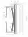
FIG. 1 is a sectioned side view of one embodiment of a fluid-dispensing chip of the invention, in an operative condition.
FIG. 2 is a sectioned side view of the fluid-dispensing chip of FIG. 1 in a quiescent condition.
FIG. 3 is a perspective cross-sectional view of another embodiment of the fluid-dispensing chip of the invention.
FIG. 4 is a close-up perspective cross-sectional view (portion A of FIG. 3), of the fluid-dispensing chip of FIG. 3.
FIG. 5 is an exploded perspective view illustrating the construction of the fluid-dispensing chip of FIG. 3.
DESCRIPTION OF PREFERRED AND OTHER EMBODIMENTS
In FIGS. 1 and 2, reference numeral 10 generally indicates a sectioned side view of one embodiment of a fluid-dispensing chip of the invention.
The fluid-dispensing chip may include a silicon wafer substrate 12. A drive circuitry layer 14 is positioned on the wafer substrate 12. The drive circuitry layer 14 is in the form of a CMOS two-level metal layer that includes the drive and control circuitry for the fluid-dispensing chip 10.
A passivation layer 16 of silicon nitride is positioned on the drive circuitry layer 14 to protect the drive circuitry layer 14. A first planar electrode 18 is embedded in the layer 16. The first planar electrode 18 is of aluminum and is connected to the drive circuitry layer 14.
The fluid-dispensing chip 10 includes a nozzle chamber wall 19 and a roof wall 20 that define a nozzle chamber 22. The roof wall 20 defines a fluid ejection port 44. A fluid-ejecting member 28 is positioned in the nozzle chamber 22. The fluid-ejecting member 28 is planar and is aligned with and parallel to the first planar electrode 18.
The fluid-ejecting member 28 is positioned on a support formation 34 that extends from the passivation layer 16. The support formation 34 is dimensioned so that the fluid-ejecting member 28 is spaced a suitable distance from the first electrode 18. The support formation 34 is configured so that an air gap 40 is encapsulated between the fluid-ejecting member 28 and the first electrode 18.
The fluid-ejecting member 28 includes a second planar electrode 24 that is positioned in the nozzle chamber 22. The second planar electrode 24 is also of aluminum and is also connected to the drive circuitry layer 14. The drive circuitry layer 14 is connected to each of the electrodes 18, 24 so that a potential can be set up between the electrodes 18, 24 so that they are attracted to one another. A layer 26 of silicon nitride is positioned on the electrode 24 to impart a resilient flexibility to the fluid-ejecting member 28. Thus, when a potential is set up between the electrodes 18, 24, the fluid-ejecting member 28 is deflected towards the first electrode 18, as shown in FIG. 1. When the potential is removed, the first electrode 18 returns to a quiescent position as shown in FIG. 2.
A layer 32 of polytetrafluoroethylene (PTFE) is positioned on the first electrode 18. A layer 36 of PTFE is positioned on the second electrode 24, intermediate the electrodes 18, 24. This ensures that the electrodes 18, 24 do not stick to one another when the fluid-ejecting member 28 is deflected towards the first electrode 18. In order further to prevent stiction between the electrodes 18, 24, a projection 38 is positioned on the fluid-ejecting member 28. The projection 38 bears against the layer 32 to ensure that there is no contact between the layers 32, 36.
The nozzle chamber wall 19 defines fluid inlet openings 30 that are in fluid communication with a fluid supply so that the nozzle chamber 22 can be supplied with fluid. Fluid flows into a space 41 defined by the roof wall 20, the nozzle chamber wall 19, the fluid-ejecting member 28 and the support formation 34. It will be appreciated that this occurs when the fluid-ejecting member 28 is drawn towards the first electrode 18. When the potential is reversed, the fluid-ejecting member 28 is urged away from the first electrode 18 so that a drop 42 of fluid is ejected from the fluid ejection port 44. The fluid-ejecting member 28 could have sufficient resilience so that a reversal of potential is not necessary. In this case, release of elastic energy as the fluid-ejecting member 28 returns to its quiescent condition ensures the ejection of the fluid drop 42.
The roof wall 20 defines a rim 46 about the fluid ejection port 44.
In FIGS. 3 to 5, reference numeral 50 generally indicates another embodiment of a fluid-dispensing chip of the invention. With reference to FIGS. 1 and 2, like reference numerals refer to like parts, unless otherwise specified.
The fluid-ejecting member 28 has a peripheral portion 52 that is positioned between the nozzle chamber wall 19 and the layer 26 of silicon nitride. A corrugated annular portion 54 is positioned adjacent to the peripheral portion 52. A fluid-ejecting portion 56 defines a remainder of the fluid-ejecting member 28.
The electrodes 18, 24 and their respective PTFE layers 32, 36 are dimensioned to define the air gap 40.
The corrugated portion 54 is configured to expand when the second electrode 24 is displaced towards the first electrode 18. The silicon nitride layer 26 imparts a resilient flexibility to the corrugated portion 54. Thus, the second electrode 24 returns to a quiescent condition when the electrical potential is removed.
The nozzle chamber wall 19 is shaped to define four radially spaced fluid inlet supply channels 58 that are in fluid communication with the space 41. These allow fluid to flow into the space 41 when the second electrode 24 is drawn towards the first electrode 18.
The nozzle chamber wall 19 defines air spaces 60 that are in fluid communication with the air gap 40. These allow the passage of air when the second electrode 24 moves towards and away from the first electrode 18.
The roof wall 20 has a plurality of etchant openings 62 defined therein to facilitate the etching of sacrificial material used in the fabrication of the chip 50. The etchant openings 62 are small enough to inhibit the passage of fluid as a result of surface tension effects.
It is important to note that the fluid-dispensing chip 10, 50 is essentially a micro-electromechanical systems (MEMS) device. A method for fabricating the device can readily be deduced from the description in referenced application no: U.S. Ser. No. 09/112,787 and in many of the other referenced applications.
Applicant envisages that the fluid-dispensing chip 10, 50 will be particularly suited for lab-on-a-chip applications. It can also be applied to DNA/RNA arrays, protein chips and sensing and dosing. The fluid-dispensing chip 10, 50 could also be used for drug delivery systems.
Numerous variations and/or modifications may be made to the present invention as shown in the preferred embodiment without departing from the spirit or scope of the invention as broadly described. The preferred embodiment is, therefore, to be considered in all respects to be illustrative and not restrictive.
Claims
I/We claim:1. A fluid ejecting integrated circuit (IC), the IC comprising:
a nozzle chamber defined by chamber side walls extending from a wafer substrate, and a roof wall provided on the chamber side walls;
a fluid ejecting member provided within the nozzle chamber between the roof wall of the nozzle chamber and the wafer substrate;
a support formation provided within the nozzle chamber and spaced inwardly away from the chamber side walls, the support formation extending from the wafer substrate to support the fluid ejecting member thereon;
a first planar electrode layered to the fluid ejecting member;
a second planar electrode layered on the wafer substrate; and
a projection provided on the first planar electrode on a side facing the second planar electrode, the projection for contacting the second planar electrode to prevent contact between the first planar electrode and the second planar electrode, wherein
the first and second planar electrode establish a potential therebetween to deform the first planar electrode towards the second planar electrode.
2. A fluid ejecting IC as claimed in claim 1, wherein the support formation is continuous and defines a sealed air chamber between the first and second planar electrodes.
3. A fluid ejecting IC as claimed in claim 1, wherein the second planar electrode is coated with a plastic layer on a side facing the first planar electrode.
4. A fluid ejecting IC as claimed in claim 1, wherein a layer of silicon nitride is provided on the first electrode.
5. A fluid ejecting IC as claimed in claim 1, wherein the roof wall defines a raised rim defining a fluid ejection port.
6. A fluid ejecting IC as claimed in claim 1, further comprising a drive circuitry layer provided on the wafer substrate.
7. A fluid ejecting IC as claimed in claim 1, further comprising a fluid inlet opening defined through the chamber side wall, the fluid inlet opening providing fluid communication into the nozzle chamber.
Images & Drawings included:


Sources:
- United States Patent and Trademark Office - verify current appl. status at the USPTO↗
Similar patent applications:
Recent applications in this class:
- » 20250267236 2025-08-21
CONVERSION BETWEEN ASPECT RATIOS IN CAMERA - » 20250220127 2025-07-03
VIDEO PROCESSING METHOD, DEVICE, EQUIPMENT, AND STORAGE MEDIA - » 20250203036 2025-06-19
VIDEO IMAGE PROCESSING METHOD AND APPARATUS, AND DEVICE AND STORAGE MEDIUM - » 20250168293 2025-05-22
Bias Lighting Effect Generation for Videos - » 20250126220 2025-04-17
IMAGING APPARATUS CAPABLE OF SWITCHING DISPLAY METHODS - » 20250106349 2025-03-27
SYSTEMS AND METHODS FOR HORIZON LEVELING VIDEOS - » 20250106348 2025-03-27
EQUITABLE PRESENCE OF COMMUNICATION SESSION ATTENDEES - » 20250071232 2025-02-27
IMAGING APPARATUS AND IMAGING SYSTEM - » 20250039327 2025-01-30
DISPLAY METHOD - » 20250030812 2025-01-23
APPLICATION OF DOLLY ZOOM EFFECT TO VIDEOS
Recent applications for this Assignee:
- » 20120141040 2012-06-07
Method of compressing sequence of strokes - » 20120140280 2012-06-07
Electronically transmitted document delivery through interaction with printed document - » 20120118965 2012-05-17
Process for decoding coded data - » 20120111939 2012-05-10
Transaction recordal method - » 20120104089 2012-05-03
Electronic pen for interacting with substrate - » 20120083252 2012-04-05
Messaging via a coded business card and mobile telephone - » 20120062953 2012-03-15
Application for generating interactive document containing advertising material - » 20120057919 2012-03-08
Pen-shaped printing device - » 20120056003 2012-03-08
Substrate having coding pattern encoding Reed-Solomon symbols - » 20120044186 2012-02-23
Handheld display device having processor for rendering display output with real-time virtual transparency and form-filling option