ITO layer structure
US20100215931A1
2010-08-26
12/000,193
2007-12-10
✅ Patent granted
US 7,867,634 B2
2011-01-11
-
-
Gwendolyn Blackwell
2027-12-10
Abstract:
A ITO layer structure, which is composed of the ITO as the outermost layer and the first anti-reflected layer on the specific side of the transparent substrate, furthermore, the second anti-reflected layer is formed on the opposite side of substrate, can improve the total transmittance.
Inventors:
- Shih-Liang Chou 5 🇹🇼 Hsin-Chu, Taiwan
- Jau-Jier Chu 6 🇹🇼 Hsin-Chu, Taiwan
- I-Wen Lee 4 🇹🇼 Hsin-Chu, Taiwan
- Po-Yao Lai 2 🇹🇼 Hsin-Chu, Taiwan
- Chien-Min Weng 5 🇹🇼 Hsin-Chu, Taiwan
- Jau-Jier Chu 1 🇹🇼 Industrial Park, Taiwan
- I-Wen Lee 1 🇹🇼 Industrial Park, Taiwan
- Shih-Liang Chou 1 🇹🇼 Industrial Park, Taiwan
- Po-Yao Lai 1 🇹🇼 Industrial Park, Taiwan
- Chien-Min Weng 1 🇹🇼 Industrial Park, Taiwan
Assignee:
- Applied Vacuum Coating Technologies Co., Ltd. 1 🇹🇼 Hsin-Chu, Taiwan
Interested in similar patents?
Get notified when new applications in this technology area are published.
Classification:
C03C17/3417 » CPC main
Surface treatment of glass, not in the form of fibres or filaments, by coating with at least two coatings having different compositions with at least two coatings of inorganic materials all coatings being oxide coatings
G02B1/115 » CPC further
Optical elements characterised by the material of which they are made; Optical coatings for optical elements; Optical coatings produced by application to, or surface treatment of, optical elements; Anti-reflection coatings using inorganic layer materials only Multilayers
C03C2217/732 » CPC further
Coatings on glass; Properties of coatings; Anti-reflective coatings with specific characteristics made of a single layer
C03C2217/948 » CPC further
Coatings on glass; Other aspects of coatings; Transparent conductive oxide layers [TCO] being part of a multilayer coating Layers comprising indium tin oxide [ITO]
C03C2218/365 » CPC further
Methods for coating glass; Aspects of methods for coating glass not covered above Coating different sides of a glass substrate
Y10T428/24975 » CPC further
Stock material or miscellaneous articles; Structurally defined web or sheet [e.g., overall dimension, etc.] including components having same physical characteristic in differing degree; Thickness [relative or absolute]; Absolute thicknesses specified No layer or component greater than 5 mils thick
Y10T428/265 » CPC further
Stock material or miscellaneous articles; Web or sheet containing structurally defined element or component, the element or component having a specified physical dimension; Coating layer not in excess of 5 mils thick or equivalent; Up to 3 mils 1 mil or less
Y10T428/31507 » CPC further
Stock material or miscellaneous articles; Composite [nonstructural laminate] Of polycarbonate
Y10T428/31935 » CPC further
Stock material or miscellaneous articles; Composite [nonstructural laminate]; Of addition polymer from unsaturated monomers Ester, halide or nitrile of addition polymer
G06F3/041 IPC
Input arrangements for transferring data to be processed into a form capable of being handled by the computer; Output arrangements for transferring data from processing unit to output unit, e.g. interface arrangements; Input arrangements or combined input and output arrangements for interaction between user and computer; Arrangements for converting the position or the displacement of a member into a coded form Digitisers, e.g. for touch screens or touch pads, characterised by the transducing means
B05D1/18 IPC
Processes for applying liquids or other fluent materials performed by dipping
B32B17/06 IPC
Layered products essentially comprising sheet glass, or glass, slag, or like fibres comprising glass as the main or only constituent of a layer, next to another layer of a specific material
B32B27/06 IPC
Layered products comprising synthetic resin as the main or only constituent of a layer, next to another layer of a
B32B7/02 IPC
Layered products characterised by the relation between layers; Layered products characterised by the relative orientation of features between layers, or by the relative values of a measurable parameter between layers, i.e. products comprising layers having different physical, chemical or physicochemical properties; Layered products characterised by the interconnection of layers Physical, chemical or physicochemical properties
B32B9/00 IPC
Layered products characterised by particular substances used
B32B9/00 IPC
Layered products comprising a layer of a particular substance not covered by groups -
Description
BACKGROUND OF THE INVENTION
(a) Field of the Invention
The present invention is related to an anti-reflection conductive coating, for plastic and/or glass substrate, whereby the structure has a high anti-reflection and/or transmittance effect. More specifically the invention is related to a layer structure which contains a transparent conductive oxide, known as Indium Tin oxide, ITO, as the outermost surface layer.
(b) Description of the Prior Art
Indium Tin Oxide (ITO) transparent conductive film is one of star products having research efforts and economic values and it is generally applied in car-laden LCD, touch panel, EMI RF shielding glass, liquid crystal wrist watch, liquid crystal panel on electric home appliance, solar cell, portable liquid crystal TV game unit, PDP, EL, LCD, and electrode for color filter.
The ITO is made by having indium oxide doped with small amount of tin oxide to have tin atoms to replace certain indium atoms existing in the structure of indium oxide. Therefore, in terms of the composition of its general structure, Indium oxide (In2O3) dominates. Indium oxide related to an oxide of semiconductor material not only presents a high band gap (Eg≧2.9 eV) for light to permeate but also contains high concentration of carriers and mobility. Of course, depending on the individual conductivity, the applied range of indium oxide varies.
Most of the applications of ITO layer structure are focus on panel or display industry products, it becomes very important to have the high transmittance property in visible light, therefore, positively searching for a good and high transmittance methods with ITO layer structure panel has been put on the top priority.
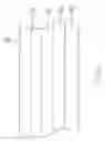
The related prior art schematically shows as FIG. 5: a transparent substrate 1, the first anti-reflected layer 2 and a transparent conductive ITO layer 3 in sequence. While some specific wavelength of visible light, such as 500 nm, transmit from the ITO layer and pass by the opposite side of substrate 1, the transmittance measured is only 94.16%. So how to improve and obtain a better transmittance of ITO layer structure is one of the most important focuses in the field of related industry.
SUMMARY OF THE INVENTION
The primary purpose of the present invention is to provide an ITO layer structure which can improve the transmittance of visible light. To achieve the purpose, an outermost layer of ITO and the first anti-reflected layer on the specific side of transparent substrate is a basic, furthermore a second anti-reflected SiO2 oxide layer formed on the opposite side of substrate is added to improve the transmittance effect.
BRIEF DESCRIPTION OF THE DRAWINGS
FIG. 1 shows a cross sectional view of ITO layer structure, which is associated as embodiment 1 of the present invention.
FIG. 2 shows a cross sectional view of ITO layer structure, which is associated as embodiment 2 of the present invention.
FIG. 3 shows a cross sectional view of ITO layer structure, which is associated as embodiment 3 of the present invention.
FIG. 4(A)-(B) shows a cross sectional view of ITO layer structure, which is associated as embodiment 4 of the present invention.
FIG. 5 shows a prior art cross sectional view of ITO layer structure.
FIG. 6 shows a cross sectional view of ITO layer structure, which is associated as embodiment 5 of the present invention.
FIG. 7 shows a cross sectional view of ITO layer structure, which is associated as embodiment 6 of the present invention.
FIG. 8 shows a cross sectional view of ITO layer structure, which is associated as embodiment 7 of the present invention.
DETAILED DESCRIPTION OF THE PREFERRED EMBODIMENTS
To obtain clearly understanding of the present invention, please consult the detail description of the drawings and embodiments.
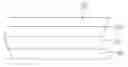
The present invention related to an ITO layer structure with high transmittance property. FIG. 1 can be taken as embodiment 1 of the present invention. An ITO layer 30 is the outermost conductive layer on the specific side of a transparent substrate 10, and a first anti-reflected layer 20 is formed between the ITO 30 and the substrate 10. Furthermore, at least a second anti-reflected layer 40 is formed on the opposite side of the substrate. Therefore, there are four layers in the structure, namely, in sequence comprising: the ITO layer 30, the first anti-reflected layer 20, the transparent substrate 10 and the second anti-reflected layer 40, wherein the second anti-reflected layer layer 40 can be processed by coating or dipping methods and the second anti-reflected layer 40 is made of SiO2, which can improve the total transmittance of the ITO layer structure.
The substrate 10 may be related to a transparent glass or plastic substrate; if the transparent glass substrate is selected, a Soda Lim Glass or a Quartz Glass is preferred; and if the transparent plastic substrate is selected from the group consisted of a Polycarbonate (PC), polymethyl methacrylate (PMMA) and Polyethylene terephthalate (PET), and PC inter alia. The ITO layer 30 has a refractive index between 1.9˜2.1 at a visible light wavelength of 520˜550 nm and a physical thickness between 10˜40 nm with a sheet resistance between 200˜1500 ohm/sq.
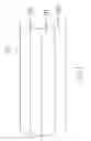
The first anti-reflected layer 20, which is formed on the substrate 10, can be performed by at least one oxide layer, showing in FIG. 2 as embodiment 2, namely in consecutive numerical order: a first oxide layer 21, a second oxide layer 22 and a third oxide layer 23, beginning from the outermost ITO layer 30. The first oxide layer 21, preferable SiO2 material, has a refractive index between 1.40˜1.50 at a visible light wavelength of 520˜550 nm and a physical thickness between 30˜60 nm; the second oxide layer 22 is selected from the group consisted of TiO2, NbO and Ta2O5, has a refractive index between 2.1˜2.3 at a visible light wavelength of 520˜550 nm and a physical thickness between 30˜80 nm; the third oxide layer 23 can be a mixture materials of SiO2 and NbO, has a refractive index between 1.9˜2.1 at a visible light wavelength of 520˜550 nm and a physical thickness between 40˜80 nm.
Either way can be performed showing in FIG. 3 as embodiment 3, namely in consecutive numerical order: a fourth oxide layer 24, a fifth oxide layer 25, a sixth oxide layer 26 and a seventh oxide layer 27, beginning from the outermost ITO layer 30. The fourth oxide layer 24, preferable SiO2 material, has a refractive index between 1.40˜1.50 at a visible light wavelength of 520˜550 nm and a physical thickness between 20˜60 nm; the fifth oxide layer 25 is selected from the group consisted of TiO2, NbO and Ta2O5, has a refractive index between 2.1˜2.3 at a visible light wavelength of 520˜550 nm and a physical thickness between 40˜90 nm; the sixth oxide layer 26, preferable SiO2 material, has a refractive index between 1.40˜1.50 at a visible light wavelength of 520˜550 nm and a physical thickness between 20˜60 nm; the seventh oxide layer 27 is selected from the group consisted of TiO2, NbO and Ta2O5, has a refractive index between 2.1˜2.3 at a visible light wavelength of 520˜550 nm and a physical thickness between 10˜40 nm.
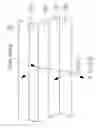
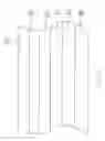
FIG. 4(A) shows as embodiment 4, the second anti-reflected layer 40 can be comprised by SiO2, which is formed on the opposite side of the ITO layer 30, can obviously improve the transmittance of the ITO layer structure. The second anti-reflected layer 40 is an oxide layer, preferable a SiO2 layer, has a refractive index between 1.40˜1.50 at a visible light wavelength of 520˜550 nm and a physical thickness between 60˜120 nm. The total transmittance measured can be improved to 97.05%. To practical perform the structure, even like FIG. 4(B) showing, the second anti-reflected layer 40 of SiO2 oxide can also be formed on the both sides of the substrate 10 at the same time, thereby, on the ITO side there can be fined the second anti-reflected layer 40 between the first anti-reflected layer 20 and the substrate 10.
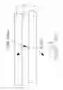
Of course, some oxide layers can also be formed between the substrate 10 and the second anti-reflected layer 40. FIG. 6 shows the ITO layer structure of embodiment 5, namely in sequence, comprising: the ITO layer 30, the first anti-reflected layer 20, the substrate 10, the second oxide layer 22 and the second ant-reflected layer 40 with a physical thickness between 20˜60 nm. FIG. 7 shows the ITO layer structure of embodiment 6, namely in sequence, comprising: the ITO layer 30, the first anti-reflected layer 20, the substrate 10, the third oxide layer 23, the second oxide layer 22 and the second ant-reflected layer 40 with a physical thickness between 20˜60 nm. After the test, the total transmittance measured can be improved to above 97.05%. Furthermore, the ITO layer structure can be applied into a touch panel display monitor.
However, it is to be noted that the preferred embodiments disclosed in the specification and the accompanying drawings are not limiting the present invention; and that any construction, installation, or characteristics that is same or similar to that of the present invention should fall within the scope of the purposes and claims of the present invention.
Claims
I claim:1. An ITO layer structure in sequence comprising:
an ITO layer;
a first anti-reflected layer;
a transparent substrate; and
a second anti-reflected layer.
2. The ITO layer structure as claimed in claim 1, wherein an another second anti-reflected layer is formed between the first anti-reflected layer and the substrate.
3. The ITO layer structure as claimed in claim 1, wherein the second anti-reflected layer is made of SiO2.
4. The ITO layer structure as claimed in claim 1, wherein the second anti-reflected layer is formed by coating process method on a surface of the transparent substrate.
5. The ITO layer structure as claimed in claim 1, wherein the second anti-reflected layer is formed by dipping process method on a surface of the transparent substrate.
6. The ITO layer structure as claimed in claim 1, wherein the transparent substrate is a glass.
7. The ITO layer structure as claimed in claim 1, wherein the transparent substrate is a plastic.
8. The ITO layer structure as claimed in claim 6, wherein the glass is a soda lime glass or quartz glass.
9. The ITO layer structure as claimed in claim 1, wherein the plastic is made of Polycarbonate (PC), PMMA or PET.
10. The ITO layer structure as claimed in claim 1, wherein the ITO layer has a refractive index between 1.9˜2.1 at a visible light wavelength of 520˜550 nm and a physical thickness between 10˜40 nm.
11. The ITO layer structure as claimed in claim 1, wherein the ITO layer has a sheet resistance between 200˜1500 ohm/sq.
12. The ITO layer structure as claimed in claim 1, wherein the first anti-reflected layer in sequence comprising:
a first oxide layer is made of SiO2 and has a refractive index between 1.40˜1.50 at a visible light wavelength of 520˜550 nm and a physical thickness between 30˜60 nm;
a second oxide layer is selected from the group consisted of TiO2, NbO and Ta2O5 and has a refractive index between 2.1˜2.3 at a visible light wavelength of 520˜550 nm and a physical thickness between 30˜80 nm; and
a third oxide layer is a mixture material of SiO2 and NbO and has a refractive index between 1.9˜2.1 at a visible light wavelength of 520˜550 nm and a physical thickness between 40˜80 nm.
13. The ITO layer structure as claimed in claim 1, wherein the first anti-reflected layer in sequence comprising:
a fourth oxide layer is made of SiO2 and has a refractive index between 1.40˜1.50 at a visible light wavelength of 520˜550 nm and a physical thickness between 20˜60 nm;
a fifth oxide layer is selected from the group consisted of TiO2, NbO and Ta2O5 and has a refractive index between 2.1˜2.3 at a visible light wavelength of 520˜550 nm and a physical thickness between 40˜90 nm;
a sixth oxide layer is made of SiO2 and has a refractive index between 1.40˜1.50 at a visible light wavelength of 520˜550 nm and a physical thickness between 20˜60 nm; and
a seventh oxide layer is selected from the group consisted of TiO2, NbO and Ta2O5 and has a refractive index between 2.1˜2.3 at a visible light wavelength of 520˜550 nm and a physical thickness between 10˜40 nm;
14. The ITO layer structure as claimed in claim 1, wherein the second anti-reflected layer is made of SiO2 and has a refractive index between 1.40˜1.50 at a visible light wavelength of 520˜550 nm and a physical thickness between 60˜120 nm.
15. The ITO layer structure as claimed in claim 1, wherein a second oxide layer is formed between the second anti-reflected layer and the substrate; wherein the second oxide layer is selected from the group consisted of TiO2, NbO and Ta2O5 and has a refractive index between 2.1˜2.3 at a visible light wavelength of 520˜550 nm and a physical thickness between 30˜80 nm.
16. The ITO layer structure as claimed in claim 15, wherein a third oxide layer is formed between the second oxide layer and the substrate; wherein the third oxide layer is a mixture material of SiO2 and NbO and has a refractive index between 1.9˜2.1 at a visible light wavelength of 520˜550 nm and a physical thickness between 40˜80 nm.
17. The ITO layer structure as claimed in claim 1, wherein the layer structure between the substrate and the second anti-reflected layer in sequence comprising:
a seventh oxide layer is selected from the group consisted of TiO2, NbO and Ta2O5 and has a refractive index between 2.1˜2.3 at a visible light wavelength of 520˜550 nm and a physical thickness between 10˜40 nm;
a sixth oxide layer is made of SiO2 and has a refractive index between 1.40˜1.50 at a visible light wavelength of 520˜550 nm and a physical thickness between 20˜60 nm; and
a fifth oxide layer is selected from the group consisted of TiO2, NbO and Ta2O5 and has a refractive index between 2.1˜2.3 at a visible light wavelength of 520˜550 nm and a physical thickness between 40˜90 nm.
18. A touch panel display monitor, which including the ITO layer structure as claim 1.
Images & Drawings included:


Sources:
- United States Patent and Trademark Office - verify current appl. status at the USPTO↗
Similar patent applications:
Recent applications in this class:
- » 20250276935 2025-09-04
GLASS STACKING, PREPARATION PROCESS THEREOF AND WINDOW ASSEMBLY COMPRISING THE GLASS STACKING - » 20250154051 2025-05-15
GLASS ARTICLE - » 20250145521 2025-05-08
PROCESS FOR FORMING A COATING - » 20240400440 2024-12-05
Coating of glass-based assembly - » 20240351942 2024-10-24
GREENHOUSE GLAZING - » 20240317640 2024-09-26
Method for preparing cover substrate - » 20240190760 2024-06-13
GREENHOUSE GLASS FOR REDUCTION OF OVERHEATING DURING THE HOT SEASONS - » 20240158294 2024-05-16
WINDSHIELD AND WINDSHIELD MANUFACTURING METHOD - » 20240034669 2024-02-01
COATED GLAZING - » 20230365459 2023-11-16
COATED GLAZING