METHOD FOR DEAD NOZZLE REMAPPING
US20100238213A1
2010-09-23
12/790,945
2010-05-31
Abstract:
A method of accounting for dead nozzle remapping in a multi-nozzle printhead includes defining a first fixative plane and a second fixative plane; determining a first color plane requiring the fixative; determining if fixative is present in the first color plane; determining if the first color plane is dead; and adding fixative to a second color plane when it is determined that the first color plane is dead.
Inventors:
- Simon Robert Walmsley 590 🇦🇺 Balmain, Australia
- Richard Thomas Plunkett 68 🇦🇺 Balmain, Australia
Interested in similar patents?
Get notified when new applications in this technology area are published.
Classification:
G06F21/73 » CPC main
Security arrangements for protecting computers, components thereof, programs or data against unauthorised activity; Protecting specific internal or peripheral components, in which the protection of a component leads to protection of the entire computer to assure secure computing or processing of information by creating or determining hardware identification, e.g. serial numbers
G06F21/554 » CPC further
Security arrangements for protecting computers, components thereof, programs or data against unauthorised activity; Monitoring users, programs or devices to maintain the integrity of platforms, e.g. of processors, firmware or operating systems; Detecting local intrusion or implementing counter-measures involving event detection and direct action
G06F21/57 » CPC further
Security arrangements for protecting computers, components thereof, programs or data against unauthorised activity; Monitoring users, programs or devices to maintain the integrity of platforms, e.g. of processors, firmware or operating systems Certifying or maintaining trusted computer platforms, e.g. secure boots or power-downs, version controls, system software checks, secure updates or assessing vulnerabilities
G06F21/575 » CPC further
Security arrangements for protecting computers, components thereof, programs or data against unauthorised activity; Monitoring users, programs or devices to maintain the integrity of platforms, e.g. of processors, firmware or operating systems; Certifying or maintaining trusted computer platforms, e.g. secure boots or power-downs, version controls, system software checks, secure updates or assessing vulnerabilities Secure boot
G06F21/64 » CPC further
Security arrangements for protecting computers, components thereof, programs or data against unauthorised activity; Protecting data Protecting data integrity, e.g. using checksums, certificates or signatures
G06F21/71 » CPC further
Security arrangements for protecting computers, components thereof, programs or data against unauthorised activity; Protecting specific internal or peripheral components, in which the protection of a component leads to protection of the entire computer to assure secure computing or processing of information
G06F21/74 » CPC further
Security arrangements for protecting computers, components thereof, programs or data against unauthorised activity; Protecting specific internal or peripheral components, in which the protection of a component leads to protection of the entire computer to assure secure computing or processing of information operating in dual or compartmented mode, i.e. at least one secure mode
G06F21/78 » CPC further
Security arrangements for protecting computers, components thereof, programs or data against unauthorised activity; Protecting specific internal or peripheral components, in which the protection of a component leads to protection of the entire computer to assure secure storage of data
H03K5/1252 » CPC further
Manipulating of pulses not covered by one of the other main groups of this subclass; Discriminating pulses Suppression or limitation of noise or interference
H04N1/405 » CPC further
Scanning, transmission or reproduction of documents or the like, e.g. facsimile transmission; Details thereof; Picture signal circuits Halftoning, i.e. converting the picture signal of a continuous-tone original into a corresponding signal showing only two levels
B41J2202/20 » CPC further
Embodiments of or processes related to ink-jet or thermal heads; Embodiments of or processes related to ink-jet heads Modules
Y10S707/99933 » CPC further
Data processing: database and file management or data structures; Database or file accessing Query processing, i.e. searching
Y10S707/99939 » CPC further
Data processing: database and file management or data structures; Database or file accessing Privileged access
Y10T29/49401 » CPC further
Metal working; Method of mechanical manufacture Fluid pattern dispersing device making, e.g., ink jet
B41J29/38 IPC
Details of, or accessories for, typewriters or selective printing mechanisms not otherwise provided for Drives, motors, controls or automatic cut-off devices for the entire printing mechanism
Description
CROSS REFERENCE TO RELATED APPLICATIONS
The present application is a Continuation of U.S. application Ser. No. 10/727,181 filed Dec. 2, 2003, all of which are herein incorporated by reference.
FIELD OF INVENTION
The present invention relates to techniques for outputting one or more lines of a dither matrix from a memory containing the dither matrix.
BACKGROUND OF INVENTION
Manufacturing a printhead that has relatively high resolution and print-speed raises a number of problems.
Difficulties in manufacturing pagewidth printheads of any substantial size arise due to the relatively small dimensions of standard silicon wafers that are used in printhead (or printhead module) manufacture. For example, if it is desired to make an 8 inch wide pagewidth printhead, only one such printhead can be laid out on a standard 8-inch wafer, since such wafers are circular in plan. Manufacturing a pagewidth printhead from two or more smaller modules can reduce this limitation to some extent, but raises other problems related to providing a joint between adjacent printhead modules that is precise enough to avoid visible artefacts (which would typically take the form of noticeable lines) when the printhead is used. The problem is exacerbated in relatively high-resolution applications because of the tight tolerances dictated by the small spacing between nozzles.
The quality of a joint region between adjacent printhead modules relies on factors including a precision with which the abutting ends of each module can be manufactured, the accuracy with which they can be aligned when assembled into a single printhead, and other more practical factors such as management of ink channels behind the nozzles. It will be appreciated that the difficulties include relative vertical displacement of the printhead modules with respect to each other.
Whilst some of these issues may be dealt with by careful design and manufacture, the level of precision required renders it relatively expensive to manufacture printheads within the required tolerances. It would be desirable to provide a solution to one or more of the problems associated with precision manufacture and assembly of multiple printhead modules to form a printhead, and especially a pagewidth printhead.
In some cases, it is desirable to produce a number of different printhead module types or lengths on a substrate to maximise usage of the substrate's surface area. However, different sizes and types of modules will have different numbers and layouts of print nozzles, potentially including different horizontal and vertical offsets. Where two or more modules are to be joined to form a single printhead, there is also the problem of dealing with different seam shapes between abutting ends of joined modules, which again may incorporate vertical or horizontal offsets between the modules. Printhead controllers are usually dedicated application specific integrated circuits (ASICs) designed for specific use with a single type of printhead module, that is used by itself rather than with other modules. It would be desirable to provide a way in which different lengths and types of printhead modules could be accounted for using a single printer controller.
In any printing system that includes multiple nozzles on a printhead or printhead module, there is the possibility of one or more of the nozzles failing in the field, or being inoperative due to manufacturing defect. Given the relatively large size of a typical printhead module, it would be desirable to provide some form of compensation for one or more “dead” nozzles. Where the printhead also outputs fixative on a per-nozzle basis, it is also desirable that the fixative is provided in such a way that dead nozzles are compensated for.
SUMMARY OF INVENTION
According to an aspect of the present disclosure, a method of accounting for dead nozzle remapping in a multi-nozzle printhead includes defining a first fixative plane and a second fixative plane; determining a first color plane requiring the fixative; determining if fixative is present in the first color plane; determining if the first color plane is dead; and adding fixative to a second color plane when it is determined that the first color plane is dead.
BRIEF DESCRIPTION OF THE DRAWINGS
Preferred and other embodiments of the invention will now be described, by way of example only, with reference to the accompanying drawings, in which:
FIG. 1 is an example of state machine notation
FIG. 2 shows document data flow in a printer
FIG. 3 is an example of a single printer controller (hereinafter “SoPEC”) A4 simplex printer system
FIG. 4 is an example of a dual SoPEC A4 duplex printer system
FIG. 5 is an example of a dual SoPEC A3 simplex printer system
FIG. 6 is an example of a quad SoPEC A3 duplex printer system
FIG. 7 is an example of a SoPEC A4 simplex printing system with an extra SoPEC used as DRAM storage
FIG. 8 is an example of an A3 duplex printing system featuring four printing SoPECs
FIG. 9 shows pages containing different numbers of bands
FIG. 10 shows the contents of a page band
FIG. 11 illustrates a page data path from host to SoPEC
FIG. 12 shows a page structure
FIG. 13 shows a SoPEC system top level partition
FIG. 14 shows a SoPEC CPU memory map (not to scale)
FIG. 15 is a block diagram of CPU
FIG. 16 shows CPU bus transactions
FIG. 17 shows a state machine for a CPU subsystem slave
FIG. 18 shows a SoPEC CPU memory map (not to scale)
FIG. 19 shows an external signal view of a memory management unit (hereinafter “MMU”) sub-block partition
FIG. 20 shows an internal signal view of an MMU sub-block partition
FIG. 21 shows a DRAM write buffer
FIG. 22 shows DIU waveforms for multiple transactions
FIG. 23 shows a SoPEC LEON CPU core
FIG. 24 shows a cache data RAM wrapper
FIG. 25 shows a realtime debug unit block diagram
FIG. 26 shows interrupt acknowledge cycles for single and pending interrupts
FIG. 27 shows an A3 duplex system featuring four printing SoPECs with a single SoPEC DRAM device
FIG. 28 is an SCB block diagram
FIG. 29 is a logical view of the SCB of FIG. 28
FIG. 30 shows an ISI configuration with four SoPEC devices
FIG. 31 shows half-duplex interleaved transmission from ISIMaster to ISISlave
FIG. 32 shows ISI transactions
FIG. 33 shows an ISI long packet
FIG. 34 shows an ISI ping packet
FIG. 35 shows a short ISI packet
FIG. 36 shows successful transmission of two long packets with sequence bit toggling
FIG. 37 shows sequence bit operation with errored long packet
FIG. 38 shows sequence bit operation with ACK error
FIG. 39 shows an ISI sub-block partition
FIG. 40 shows an ISI serial interface engine functional block diagram
FIG. 41 is an SIE edge detection and data IO diagram
FIG. 42 is an SIE Rx/Tx state machine Tx cycle state diagram
FIG. 43 shows an SIE Rx/Tx state machine Tx bit stuff ‘0’ cycle state diagram
FIG. 44 shows an SIE Rx/Tx state machine Tx bit stuff ‘1’ cycle state diagram
FIG. 45 shows an SIE Rx/Tx state machine Rx cycle state diagram
FIG. 46 shows an SIE Tx functional timing example
FIG. 47 shows an SIE Rx functional timing example
FIG. 48 shows an SIE Rx/Tx FIFO block diagram
FIG. 49 shows SIE Rx/Tx FIFO control signal gating
FIG. 50 shows an SIE bit stuffing state machine Tx cycle state diagram
FIG. 51 shows an SIE bit stripping state machine Rx cycle state diagram
FIG. 52 shows a CRC 16 generation/checking shift register
FIG. 53 shows circular buffer operation
FIG. 54 shows duty cycle select
FIG. 55 shows a GPIO partition
FIG. 56 shows a motor control RTL diagram
FIG. 57 is an input de-glitch RTL diagram
FIG. 58 is a frequency analyser RTL diagram
FIG. 59 shows a brushless DC controller
FIG. 60 shows a period measure unit
FIG. 61 shows line synch generation logic
FIG. 62 shows an ICU partition
FIG. 63 is an interrupt clear state diagram
FIG. 63A Timers sub-block partition diagram
FIG. 64 is a watchdog timer RTL diagram
FIG. 65 is a generic timer RTL diagram
FIG. 66 is a schematic of a timing pulse generator
FIG. 67 is a Pulse generator RTL diagram
FIG. 68 shows a SoPEC clock relationship
FIG. 69 shows a CPR block partition
FIG. 70 shows reset deglitch logic
FIG. 71 shows reset synchronizer logic
FIG. 72 is a clock gate logic diagram
FIG. 73 shows a PLL and Clock divider logic
FIG. 74 shows a PLL control state machine diagram
FIG. 75 shows a LSS master system-level interface
FIG. 76 shows START and STOP conditions
FIG. 77 shows an LSS transfer of 2 data bytes
FIG. 78 is an example of an LSS write to a QA Chip
FIG. 79 is an example of an LSS read from QA Chip
FIG. 80 shows an LSS block diagram
FIG. 81 shows an LSS multi-command transaction
FIG. 82 shows start and stop generation based on previous bus state
FIG. 83 shows an LSS master state machine
FIG. 84 shows LSS master timing
FIG. 85 shows a SoPEC system top level partition
FIG. 86 shows an ead bus with 3 cycle random DRAM read accesses
FIG. 87 shows interleaving of CPU and non-CPU read accesses
FIG. 88 shows interleaving of read and write accesses with 3 cycle random DRAM accesses
FIG. 89 shows interleaving of write accesses with 3 cycle random DRAM accesses
FIG. 90 shows a read protocol for a SoPEC Unit making a single 256-bit access
FIG. 91 shows a read protocol for a SoPEC Unit making a single 256-bit access
FIG. 92 shows a write protocol for a SoPEC Unit making a single 256-bit access
FIG. 93 shows a protocol for a posted, masked, 128-bit write by the CPU
FIG. 94 shows a write protocol shown for CDU making four contiguous 64-bit accesses
FIG. 95 shows timeslot-based arbitration
FIG. 96 shows timeslot-based arbitration with separate pointers
FIG. 97 shows a first example (a) of separate read and write arbitration
FIG. 98 shows a second example (b) of separate read and write arbitration
FIG. 99 shows a third example (c) of separate read and write arbitration
FIG. 100 shows a DIU partition
FIG. 101 shows a DIU partition
FIG. 102 shows multiplexing and address translation logic for two memory instances
FIG. 103 shows a timing of dau dcu valid, dcu dau adv and dcu dau wady
FIG. 104 shows a DCU state machine
FIG. 105 shows random read timing
FIG. 106 shows random write timing
FIG. 107 shows refresh timing
FIG. 108 shows page mode write timing
FIG. 109 shows timing of non-CPU DIU read access
FIG. 110 shows timing of CPU DIU read access
FIG. 111 shows a CPU DIU read access
FIG. 112 shows timing of CPU DIU write access
FIG. 113 shows timing of a non-CDU/non-CPU DIU write access
FIG. 114 shows timing of CDU DIU write access
FIG. 115 shows command multiplexor sub-block partition
FIG. 116 shows command multiplexor timing at DIU requestors interface
FIG. 117 shows generation of re arbitrate and re arbitrate wady
FIG. 118 shows CPU interface and arbitration logic
FIG. 119 shows arbitration timing
FIG. 120 shows setting RotationSync to enable a new rotation.
FIG. 121 shows a timeslot based arbitration
FIG. 122 shows a timeslot based arbitration with separate pointers
FIG. 123 shows a CPU pre-access write lookahead pointer
FIG. 124 shows arbitration hierarchy
FIG. 125 shows hierarchical round-robin priority comparison
FIG. 126 shows a read multiplexor partition
FIG. 127 shows a read command queue (4 deep buffer)
FIG. 128 shows state-machines for shared read bus accesses
FIG. 129 shows a write multiplexor partition
FIG. 130 shows a read multiplexer timing for back-to-back shared read bus transfer
FIG. 131 shows a write multiplexer partition
FIG. 132 shows a block diagram of a PCU
FIG. 133 shows PCU accesses to PEP registers
FIG. 134 shows command arbitration and execution
FIG. 135 shows DRAM command access state machine
FIG. 136 shows an outline of contone data flow with respect to CDU
FIG. 137 shows a DRAM storage arrangement for a single line of JPEG 8×8 blocks in 4 colors
FIG. 138 shows a read control unit state machine
FIG. 139 shows a memory arrangement of JPEG blocks
FIG. 140 shows a contone data write state machine
FIG. 141 shows lead-in and lead-out clipping of contone data in multi-SoPEC environment
FIG. 142 shows a block diagram of CFU
FIG. 143 shows a DRAM storage arrangement for a single line of JPEG blocks in 4 colors
FIG. 144 shows a block diagram of color space converter
FIG. 145 shows a converter/invertor
FIG. 146 shows a high-level block diagram of LBD in context
FIG. 147 shows a schematic outline of the LBD and the SFU
FIG. 148 shows a block diagram of lossless bi-level decoder
FIG. 149 shows a stream decoder block diagram
FIG. 150 shows a command controller block diagram
FIG. 151 shows a state diagram for command controller (CC) state machine
FIG. 152 shows a next edge unit block diagram
FIG. 153 shows a next edge unit buffer diagram
FIG. 154 shows a next edge unit edge detect diagram
FIG. 155 shows a state diagram for the next edge unit state machine
FIG. 156 shows a line fill unit block diagram
FIG. 157 shows a state diagram for the Line Fill Unit (LFU) state machine
FIG. 158 shows a bi-level DRAM buffer
FIG. 159 shows interfaces between LBD/SFU/HCU
FIG. 160 shows an SFU sub-block partition
FIG. 161 shows an LBDPrevLineFifo sub-block
FIG. 162 shows timing of signals on the LBDPrevLineFIFO interface to DIU and address generator
FIG. 163 shows timing of signals on LBDPrevLineFIFO interface to DIU and address generator
FIG. 164 shows LBDNextLineFifo sub-block
FIG. 165 shows timing of signals on LBDNextLineFIFO interface to DIU and address generator
FIG. 166 shows LBDNextLineFIFO DIU interface state diagram
FIG. 167 shows an LDB to SFU write interface
FIG. 168 shows an LDB to SFU read interface (within a line)
FIG. 169 shows an HCUReadLineFifo Sub-block
FIG. 170 shows a DIU write Interface
FIG. 171 shows a DIU Read Interface multiplexing by select_hrfplf
FIG. 172 shows DIU read request arbitration logic
FIG. 173 shows address generation
FIG. 174 shows an X scaling control unit
FIG. 175 Y shows a scaling control unit
FIG. 176 shows an overview of X and Y scaling at HCU interface
FIG. 177 shows a high level block diagram of TE in context
FIG. 178 shows a QR Code
FIG. 179 shows Netpage tag structure
FIG. 180 shows a Netpage tag with data rendered at 1600 dpi (magnified view)
FIG. 181 shows an example of 2×2 dots for each block of QR code
FIG. 182 shows placement of tags for portrait & landscape printing
FIG. 183 shows agGeneral representation of tag placement
FIG. 184 shows composition of SoPEC's tag format structure
FIG. 185 shows a simple 3×3 tag structure
FIG. 186 shows 3×3 tag redesigned for 21×21 area (not simple replication)
FIG. 187 shows a TE Block Diagram
FIG. 188 shows a TE Hierarchy
FIG. 189 shows a block diagram of PCU accesses
FIG. 190 shows a tag encoder top-level FSM
FIG. 191 shows generated control signals
FIG. 192 shows logic to combine dot information and encoded data
FIG. 193 shows generation of Lastdotintag/1
FIG. 194 shows generation of Dot Position Valid
FIG. 195 shows generation of write enable to the TFU
FIG. 196 shows generation of Tag Dot Number
FIG. 197 shows TDI Architecture
FIG. 198 shows data flow through the TDI
FIG. 199 shows raw tag data interface block diagram
FIG. 200 shows an RTDI State Flow Diagram
FIG. 201 shows a relationship between TE_endoftagdata, cdu_startofbandstore and cdu_endofbandstore
FIG. 202 shows a TDi State Flow Diagram
FIG. 203 shows mapping of the tag data to codewords 0-7
FIG. 204 shows coding and mapping of uncoded fixed tag data for (15,5) RS encoder
FIG. 205 shows mapping of pre-coded fixed tag data
FIG. 206 shows coding and mapping of variable tag data for (15,7) RS encoder
FIG. 207 shows coding and mapping of uncoded fixed tag data for (15,7) RS encoder
FIG. 208 shows mapping of 2D decoded variable tag data
FIG. 209 shows a simple block diagram for an m=4 Reed Solomon encoder
FIG. 210 shows an RS encoder I/O diagram
FIG. 211 shows a (15,5) & (15,7) RS encoder block diagram
FIG. 212 shows a (15,5) RS encoder timing diagram
FIG. 213 shows a (15,7) RS encoder timing diagram
FIG. 214 shows a circuit for multiplying by alpha3
FIG. 215 shows adding two field elements
FIG. 216 shows an RS encoder implementation
FIG. 217 shows an encoded tag data interface
FIG. 218 shows an encoded fixed tag data interface
FIG. 219 shows an encoded variable tag data interface
FIG. 220 shows an encoded variable tag data sub-buffer
FIG. 221 shows a breakdown of the tag format structure
FIG. 222 shows a TFSI FSM state flow diagram
FIG. 223 shows a TFS block diagram
FIG. 224 shows a table A interface block diagram
FIG. 225 shows a table A address generator
FIG. 226 shows a table C interface block diagram
FIG. 227 shows a table B interface block diagram
FIG. 228 shows interfaces between TE, TFU and HCU
FIG. 229 shows a 16-byte FIFO in TFU
FIG. 230 shows a high level block diagram showing the HCU and its external interfaces
FIG. 231 shows a block diagram of the HCU
FIG. 232 shows a block diagram of the control unit
FIG. 233 shows a block diagram of determine advdot unit
FIG. 234 shows a page structure
FIG. 235 shows a block diagram of a margin unit
FIG. 236 shows a block diagram of a dither matrix table interface
FIG. 237 shows an example of reading lines of dither matrix from DRAM
FIG. 238 shows a state machine to read dither matrix table
FIG. 239 shows a contone dotgen unit
FIG. 240 shows a block diagram of dot reorg unit
FIG. 241 shows an HCU to DNC interface (also used in DNC to DWU, LLU to PHI)
FIG. 242 shows SFU to HCU interface (all feeders to HCU)
FIG. 243 shows representative logic of the SFU to HCU interface
FIG. 244 shows a high-level block diagram of DNC
FIG. 245 shows a dead nozzle table format
FIG. 246 shows set of dots operated on for error diffusion
FIG. 247 shows a block diagram of DNC
FIG. 248 shows a sub-block diagram of ink replacement unit
FIG. 249 shows a dead nozzle table state machine
FIG. 250 shows logic for dead nozzle removal and ink replacement
FIG. 251 shows a sub-block diagram of error diffusion unit
FIG. 252 shows a maximum length 32-bit LFSR used for random bit generation
FIG. 253 shows a high-level data flow diagram of DWU in context
FIG. 254 shows a printhead nozzle layout for 36-nozzle bi-lithic printhead
FIG. 255 shows a printhead nozzle layout for a 36-nozzle bi-lithic printhead
FIG. 256 shows a dot line store logical representation
FIG. 257 shows a conceptual view of printhead row alignment
FIG. 258 shows a conceptual view of printhead rows (as seen by the LLU and PHI)
FIG. 259 shows a comparison of 1.5×v 2× buffering
FIG. 260 shows an even dot order in DRAM (increasing sense, 13320 dot wide line)
FIG. 261 shows an even dot order in DRAM (decreasing sense, 13320 dot wide line)
FIG. 262 shows a dotline FIFO data structure in DRAM
FIG. 263 shows a DWU partition
FIG. 264 shows a buffer address generator sub-block
FIG. 265 shows a DIU Interface sub-block
FIG. 266 shows an interface controller state diagram
FIG. 267 shows a high level data flow diagram of LLU in context
FIG. 268 shows paper and printhead nozzles relationship (example with D1=D2=5)
FIG. 269 shows printhead structure and dot generate order
FIG. 270 shows an order of dot data generation and transmission
FIG. 271 shows a conceptual view of printhead rows
FIG. 272 shows a dotline FIFO data structure in DRAM (LLU specification)
FIG. 273 shows an LLU partition
FIG. 274 shows a dot generator RTL diagram
FIG. 275 shows a DIU interface
FIG. 276 shows an interface controller state diagram
FIG. 277 shows high-level data flow diagram of PHI in context
FIG. 278 shows power on reset
FIG. 279 shows printhead data rate equalization
FIG. 280 shows a printhead structure and dot generate order
FIG. 281 shows an order of dot data generation and transmission
FIG. 282 shows an order of dot data generation and transmission (single printhead case)
FIG. 283 shows printhead interface timing parameters
FIG. 284 shows printhead timing with margining
FIG. 285 shows a PHI block partition
FIG. 286 shows a sync generator state diagram
FIG. 287 shows a line sync de-glitch RTL diagram
FIG. 288 shows a fire generator state diagram
FIG. 289 shows a PHI controller state machine
FIG. 290 shows a datapath unit partition
FIG. 291 shows a dot order controller state diagram
FIG. 292 shows a data generator state diagram
FIG. 293 shows data serializer timing
FIG. 294 shows a data serializer RTL Diagram
FIG. 295 shows printhead types 0 to 7
FIG. 296 shows an ideal join between two dilithic printhead segments
FIG. 297 shows an example of a join between two bilithic printhead segments
FIG. 298 shows printable vs non-printable area under new definition (looking at colors as if 1 row only)
FIG. 299 shows identification of printhead nozzles and shift-register sequences for printheads in arrangement 1
FIG. 300 shows demultiplexing of data within the printheads in arrangement 1
FIG. 301 shows double data rate signalling for a type 0 printhead in arrangement 1
FIG. 302 shows double data rate signalling for a type 1 printhead in arrangement 1
FIG. 303 shows identification of printheads nozzles and shift-register sequences for printheads in arrangement 2
FIG. 304 shows demultiplexing of data within the printheads in arrangement 2
FIG. 305 shows double data rate signalling for a type 0 printhead in arrangement 2
FIG. 306 shows double data rate signalling for a type 1 printhead in arrangement 2
FIG. 307 shows all 8 printhead arrangements
FIG. 308 shows a printhead structure
FIG. 309 shows a column Structure
FIG. 310 shows a printhead dot shift register dot mapping to page
FIG. 311 shows data timing during printing
FIG. 312 shows print quality
FIG. 313 shows fire and select shift register setup for printing
FIG. 314 shows a fire pattern across butt end of printhead chips
FIG. 315 shows fire pattern generation
FIG. 316 shows determination of select shift register value
FIG. 317 shows timing for printing signals
FIG. 318 shows initialisation of printheads
FIG. 319 shows a nozzle test latching circuit
FIG. 320 shows nozzle testing
FIG. 321 shows a temperature reading
FIG. 322 shows CMOS testing
FIG. 323 shows a reticle layout
FIG. 324 shows a stepper pattern on Wafer
FIG. 325 shows relationship between datasets
FIG. 326 shows a validation hierarchy
FIG. 327 shows development of operating system code
FIG. 328 shows protocol for directly verifying reads from ChipR
FIG. 329 shows a protocol for signature translation protocol
FIG. 330 shows a protocol for a direct authenticated write
FIG. 331 shows an alternative protocol for a direct authenticated write
FIG. 332 shows a protocol for basic update of permissions
FIG. 333 shows a protocol for a multiple-key update
FIG. 334 shows a protocol for a single-key authenticated read
FIG. 335 shows a protocol for a single-key authenticated write
FIG. 336 shows a protocol for a single-key update of permissions
FIG. 337 shows a protocol for a single-key update
FIG. 338 shows a protocol for a multiple-key single-M authenticated read
FIG. 339 shows a protocol for a multiple-key authenticated write
FIG. 340 shows a protocol for a multiple-key update of permissions
FIG. 341 shows a protocol for a multiple-key update
FIG. 342 shows a protocol for a multiple-key multiple-M authenticated read
FIG. 343 shows a protocol for a multiple-key authenticated write
FIG. 344 shows a protocol for a multiple-key update of permissions
FIG. 345 shows a protocol for a multiple-key update
FIG. 346 shows relationship of permissions bits to M[n] access bits
FIG. 347 shows 160-bit maximal period LFSR
FIG. 348 shows clock filter
FIG. 349 shows tamper detection line
FIG. 350 shows an oversize nMOS transistor layout of Tamper Detection Line
FIG. 351 shows a Tamper Detection Line
FIG. 352 shows how Tamper Detection Lines cover the Noise Generator
FIG. 353 shows a prior art FET Implementation of CMOS inverter
FIG. 354 shows non-flashing CMOS
FIG. 355 shows components of a printer-based refill device
FIG. 356 shows refilling of printers by printer-based refill device
FIG. 357 shows components of a home refill station
FIG. 358 shows a three-ink reservoir unit
FIG. 359 shows refill of ink cartridges in a home refill station
FIG. 360 shows components of a commercial refill station
FIG. 361 shows an ink reservoir unit
FIG. 362 shows refill of ink cartridges in a commercial refill station (showing a single refill unit)
FIG. 363 shows equivalent signature generation
FIG. 364 shows a basic field definition
FIG. 365 shows an example of defining field sizes and positions
FIG. 366 shows permissions
FIG. 367 shows a first example of permissions for a field
FIG. 368 shows a second example of permissions for a field
FIG. 369 shows field attributes
FIG. 370 shows an output signature generation data format for Read
FIG. 371 shows an input signature verification data format for Test
FIG. 372 shows an output signature generation data format for Translate
FIG. 373 shows an input signature verification data format for WriteAuth
FIG. 374 shows input signature data format for ReplaceKey
FIG. 375 shows a key replacement map
FIG. 376 shows a key replacement map after K1 is replaced
FIG. 377 shows a key replacement process
FIG. 378 shows an output signature data format for GetProgramKey
FIG. 379 shows transfer and rollback process
FIG. 380 shows an upgrade flow
FIG. 381 shows authorised ink refill paths in the printing system
FIG. 382 shows an input signature verification data format for XferAmount
FIG. 383 shows a transfer and rollback process
FIG. 384 shows an upgrade flow
FIG. 385 shows authorised upgrade paths in the printing system
FIG. 386 shows a direct signature validation sequence
FIG. 387 shows signature validation using translation
FIG. 388 shows setup of preauth field attributes
FIG. 389 shows a high level block diagram of QA Chip
FIG. 390 shows an analogue unit
FIG. 391 shows a serial bus protocol for trimming
FIG. 392 shows a block diagram of a trim unit
FIG. 393 shows a block diagram of a CPU of the QA chip
FIG. 394 shows block diagram of an MIU
FIG. 395 shows a block diagram of memory components
FIG. 396 shows a first byte sent to an IOU
FIG. 397 shows a block diagram of the IOU
FIG. 398 shows a relationship between external SDa and SCIk and generation of internal signals
FIG. 399 shows block diagram of ALU
FIG. 400 shows a block diagram of DataSel
FIG. 401 shows a block diagram of ROR
FIG. 402 shows a block diagram of the ALU's IO block
FIG. 403 shows a block diagram of PCU
FIG. 404 shows a block diagram of an Address Generator Unit
FIG. 405 shows a block diagram for a Counter Unit
FIG. 406 shows a block diagram of PMU
FIG. 407 shows a state machine for PMU
FIG. 408 shows a block diagram of MRU
FIG. 409 shows simplified MAU state machine
FIG. 410 shows power-on reset behaviour
FIG. 411 shows a ring oscillator block diagram
FIG. 412 shows a system clock duty cycle
DETAILED DESCRIPTION
1 Print System Overview
1.1 Printing Considerations
A bi-lithic printhead produces 1600 dpi bi-level dots. On low-diffusion paper, each ejected drop forms a 22.5 μm diameter dot. Dots are easily produced in isolation, allowing dispersed-dot dithering to be exploited to its fullest. Since the bi-lithic printhead is the width of the page and operates with a constant paper velocity, color planes are printed in perfect registration, allowing ideal dot-on-dot printing. Dot-on-dot printing minimizes ‘muddying’ of midtones caused by inter-color bleed.
A page layout may contain a mixture of images, graphics and text. Continuous-tone (contone) images and graphics are reproduced using a stochastic dispersed-dot dither. Unlike a clustered-dot (or amplitude-modulated) dither, a dispersed-dot (or frequency-modulated) dither reproduces high spatial frequencies (i.e. image detail) almost to the limits of the dot resolution, while simultaneously reproducing lower spatial frequencies to their full color depth, when spatially integrated by the eye. A stochastic dither matrix is carefully designed to be free of objectionable low-frequency patterns when tiled across the image. As such its size typically exceeds the minimum size required to support a particular number of intensity levels (e.g. 16×16×8 bits for 257 intensity levels).
Human contrast sensitivity peaks at a spatial frequency of about 3 cycles per degree of visual field and then falls off logarithmically, decreasing by a factor of 100 beyond about 40 cycles per degree and becoming immeasurable beyond 60 cycles per degree. At a normal viewing distance of 12 inches (about 300 mm), this translates roughly to 200-300 cycles per inch (cpi) on the printed page, or 400-600 samples per inch according to Nyquist's theorem.
In practice, contone resolution above about 300 ppi is of limited utility outside special applications such as medical imaging. Offset printing of magazines, for example, uses contone resolutions in the range 150 to 300 ppi. Higher resolutions contribute slightly to color error through the dither.
Black text and graphics are reproduced directly using bi-level black dots, and are therefore not anti-aliased (i.e. low-pass filtered) before being printed. Text should therefore be supersampled beyond the perceptual limits discussed above, to produce smoother edges when spatially integrated by the eye. Text resolution up to about 1200 dpi continues to contribute to perceived text sharpness (assuming low-diffusion paper, of course).
A Netpage printer, for example, may use a contone resolution of 267 ppi (i.e. 1600 dpi 6), and a black text and graphics resolution of 800 dpi. A high end office or departmental printer may use a contone resolution of 320 ppi (1600 dpi/5) and a black text and graphics resolution of 1600 dpi. Both formats are capable of exceeding the quality of commercial (offset) printing and photographic reproduction.
1.2 Document Data Flow
Because of the page-width nature of the bi-lithic printhead, each page must be printed at a constant speed to avoid creating visible artifacts. This means that the printing speed cannot be varied to match the input data rate. Document rasterization and document printing are therefore decoupled to ensure the printhead has a constant supply of data. A page is never printed until it is fully rasterized. This can be achieved by storing a compressed version of each rasterized page image in memory.
This decoupling also allows the RIP(s) to run ahead of the printer when rasterizing simple pages, buying time to rasterize more complex pages.
Because contone color images are reproduced by stochastic dithering, but black text and line graphics are reproduced directly using dots, the compressed page image format contains a separate foreground bi-level black layer and background contone color layer. The black layer is composited over the contone layer after the contone layer is dithered (although the contone layer has an optional black component). A final layer of Netpage tags (in infrared or black ink) is optionally added to the page for printout.
FIG. 2 shows the flow of a document from computer system to printed page.
At 267 ppi for example, a A4 page (8.26 inches×11.7 inches) of contone CMYK data has a size of 26.3 MB. At 320 ppi, an A4 page of contone data has a size of 37.8 MB. Using lossy contone compression algorithms such as JPEG, contone images compress with a ratio up to 10:1 without noticeable loss of quality, giving compressed page sizes of 2.63 MB at 267 ppi and 3.78 MB at 320 ppi.
At 800 dpi, a A4 page of bi-level data has a size of 7.4 MB. At 1600 dpi, a Letter page of bi-level data has a size of 29.5 MB. Coherent data such as text compresses very well. Using lossless bi-level compression algorithms such as SMG4 fax, ten-point plain text compresses with a ratio of about 50:1. Lossless bi-level compression across an average page is about 20:1 with 10:1 possible for pages which compress poorly. The requirement for SoPEC is to be able to print text at 10:1 compression. Assuming 10:1 compression gives compressed page sizes of 0.74 MB at 800 dpi, and 2.95 MB at 1600 dpi.
Once dithered, a page of CMYK contone image data consists of 116 MB of bi-level data. Using lossless bi-level compression algorithms on this data is pointless precisely because the optimal dither is stochastic—i.e. since it introduces hard-to-compress disorder.
Netpage tag data is optionally supplied with the page image. Rather than storing a compressed bi-level data layer for the Netpage tags, the tag data is stored in its raw form. Each tag is supplied up to 120 bits of raw variable data (combined with up to 56 bits of raw fixed data) and covers up to a 6 mm×6 mm area (at 1600 dpi). The absolute maximum number of tags on a A4 page is 15,540 when the tag is only 2 mm×2 mm (each tag is 126 dots×126 dots, for a total coverage of 148 tags×105 tags). 15,540 tags of 128 bits per tag gives a compressed tag page size of 0.24 MB.
The multi-layer compressed page image format therefore exploits the relative strengths of lossy JPEG contone image compression, lossless bi-level text compression, and tag encoding. The format is compact enough to be storage-efficient, and simple enough to allow straightforward real-time expansion during printing.
Since text and images normally don't overlap, the normal worst-case page image size is image only, while the normal best-case page image size is text only. The addition of worst case Netpage tags adds 0.24 MB to the page image size. The worst-case page image size is text over image plus tags. The average page size assumes a quarter of an average page contains images.
The Host PC rasterizes and compresses the incoming document on a page by page basis. The page is restructured into bands with one or more bands used to construct a page. The compressed data is then transferred to the SoPEC device via the USB link. A complete band is stored in SoPEC embedded memory. Once the band transfer is complete the SoPEC device reads the compressed data, expands the band, normalizes contone, bi-level and tag data to 1600 dpi and transfers the resultant calculated dots to the bi-lithic printhead.
The document data flow is:
-
- The RIP software rasterizes each page description and compress the rasterized page image.
- The infrared layer of the printed page optionally contains encoded Netpage tags at a programmable density.
- The compressed page image is transferred to the SoPEC device via the USB normally on a band by band basis.
- The print engine takes the compressed page image and starts the page expansion.
- The first stage page expansion consists of 3 operations performed in parallel
- expansion of the JPEG-compressed contone layer
- expansion of the SMG4 fax compressed bi-level layer
- encoding and rendering of the bi-level tag data.
- The second stage dithers the contone layer using a programmable dither matrix, producing up to four bi-level layers at full-resolution.
- The second stage then composites the bi-level tag data layer, the bi-level SMG4 fax de-compressed layer and up to four bi-level JPEG de-compressed layers into the full-resolution page image.
- A fixative layer is also generated as required.
- The last stage formats and prints the bi-level data through the bi-lithic printhead via the printhead interface.
The SoPEC device can print a full resolution page with 6 color planes. Each of the color planes can be generated from compressed data through any channel (either JPEG compressed, bi-level SMG4 fax compressed, tag data generated, or fixative channel created) with a maximum number of 6 data channels from page RIP to bi-lithic printhead color planes.
The mapping of data channels to color planes is programmable, this allows for multiple color planes in the printhead to map to the same data channel to provide for redundancy in the printhead to assist dead nozzle compensation.
Also a data channel could be used to gate data from another data channel. For example in stencil mode, data from the bilevel data channel at 1600 dpi can be used to filter the contone data channel at 320 dpi, giving the effect of 1600 dpi contone image.
1.2.1 Page Considerations Due to SoPEC
The SoPEC device typically stores a complete page of document data on chip. The amount of storage available for compressed pages is limited to 2 Mbytes, imposing a fixed maximum on compressed page size. A comparison of the compressed image sizes in the following table indicates that SoPEC would not be capable of printing worst case pages unless they are split into bands and printing commences before all the bands for the page have been downloaded. The page sizes in the table are shown for comparison purposes and would be considered reasonable for a professional level printing system. The SoPEC device is aimed at the consumer level and would not be required to print pages of that complexity.
| Size | ||
| Page Content Description | Calculation | (MByte) |
| Best Case picture Image, | 8.26 × 11.7 × 267 × | 1.97 |
| 267 ppi with 3 colors, | 267 × 3 @ 10:1 | |
| A4 size | ||
| Full page text, 800 dpi | 8.26 × 11.7 × 800 × | 0.74 |
| A4 size | 800 @ 10:1 | |
| Mixed Graphics and Text | 6 × 4 × 267 × 267 × | 1.55 |
| Image of 6 inches × 4 | 3 @ 5:1 | |
| inches @ 267 ppi and | 800 × 800 × 73 @ 10:1 | |
| 3 colors | ||
| Remaining area text ~73 | ||
| inches2, 800 dpi | ||
| Best Case Photo, 3 Colors, | 6.6 Mpixel @ 10:1 | 2.00 |
| 6.6 MegaPixel Image | ||
If a document with more complex pages is required, the page RIP software in the host PC can determine that there is insufficient memory storage in the SoPEC for that document. In such cases the RIP software can take two courses of action. It can increase the compression ratio until the compressed page size will fit in the SoPEC device, at the expense of document quality, or divide the page into bands and allow SoPEC to begin printing a page band before all bands for that page are downloaded. Once SoPEC starts printing a page it cannot stop, if SoPEC consumes compressed data faster than the bands can be downloaded a buffer underrun error could occur causing the print to fail. A buffer underrun occurs if a line synchronisation pulse is received before a line of data has been transferred to the printhead.
Other options which can be considered if the page does not fit completely into the compressed page store are to slow the printing or to use multiple SoPECs to print parts of the page. A Storage SoPEC could be added to the system to provide guaranteed bandwidth data delivery. The print system could also be constructed using an ISI-Bridge chip to provide guaranteed data delivery.
1.3 Page Format and Printflow
When rendering a page, the RIP produces a page header and a number of bands (a non-blank page requires at least one band) for a page. The page header contains high level rendering parameters, and each band contains compressed page data. The size of the band will depend on the memory available to the RIP, the speed of the RIP, and the amount of memory remaining in SoPEC while printing the previous band(s). FIG. 9 shows the high level data structure of a number of pages with different numbers of bands in the page.
Each compressed band contains a mandatory band header, an optional bi-level plane, optional sets of interleaved contone planes, and an optional tag data plane (for Netpage enabled applications). Since each of these planes is optional1, the band header specifies which planes are included with the band. FIG. 10 gives a high-level breakdown of the contents of a page band. 1Although a band must contain at least one plane
A single SoPEC has maximum rendering restrictions as follows:
-
- 1 bi-level plane
- 1 contone interleaved plane set containing a maximum of 4 contone planes
- 1 tag data plane
- a bi-lithic printhead with a maximum of 2 printhead ICs
The requirement for single-sided A4 single SoPEC printing is
-
- average contone JPEG compression ratio of 10:1, with a local minimum compression ratio of 5:1 for a single line of interleaved JPEG blocks.
- average bi-level compression ratio of 10:1, with a local minimum compression ratio of 1:1 for a single line.
If the page contains rendering parameters that exceed these specifications, then the RIP or the Host PC must split the page into a format that can be handled by a single SoPEC.
In the general case, the SoPEC CPU must analyze the page and band headers and generate an appropriate set of register write commands to configure the units in SoPEC for that page. The various bands are passed to the destination SoPEC(s) to locations in DRAM determined by the host.
The host keeps a memory map for the DRAM, and ensures that as a band is passed to a SoPEC, it is stored in a suitable free area in DRAM. Each SoPEC is connected to the ISI bus or USB bus via its Serial communication Block (SCB). The SoPEC CPU configures the SCB to allow compressed data bands to pass from the USB or ISI through the SCB to SoPEC DRAM. FIG. 11 shows an example data flow for a page destined to be printed by a single SoPEC. Band usage information is generated by the individual SoPECs and passed back to the host.
SoPEC has an addressing mechanism that permits circular band memory allocation, thus facilitating easy memory management. However it is not strictly necessary that all bands be stored together. As long as the appropriate registers in SoPEC are set up for each band, and a given band is contiguous2, the memory can be allocated in any way. 2Contiguous allocation also includes wrapping around in SoPEC's band store memory.
1.4 SoPEC ASIC
The Small Office Home Office Print Engine Controller (SoPEC) is a page rendering engine ASIC that takes compressed page images as input, and produces decompressed page images at up to 6 channels of bi-level dot data as output. The bi-level dot data is generated for the Memjet bi-lithic printhead. The dot generation process takes account of printhead construction, dead nozzles, and allows for fixative generation.
A single SoPEC can control 2 bi-lithic printheads and up to 6 color channels at 10,000 lines/sec3, equating to 30 pages per minute. A single SoPEC can perform full-bleed printing of A3, A4 and Letter pages. The 6 channels of colored ink are the expected maximum in a consumer SOHO, or office Bi-lithic printing environment: 310,000 lines per second equates to 30 A4/Letter pages per minute at 1600 dpi
-
- CMY, for regular color printing.
- K, for black text, line graphics and gray-scale printing.
- IR (infrared), for Netpage-enabled applications.
- F (fixative), to enable printing at high speed. Because the bi-lithic printer is capable of printing so fast, a fixative may be required to enable the ink to dry before the page touches the page already printed. Otherwise the pages may bleed on each other. In low speed printing environments the fixative may not be required.
SoPEC is color space agnostic. Although it can accept contone data as CMYX or RGBX, where X is an optional 4th channel, it also can accept contone data in any print color space. Additionally, SoPEC provides a mechanism for arbitrary mapping of input channels to output channels, including combining dots for ink optimization, generation of channels based on any number of other channels etc. However, inputs are typically CMYK for contone input, K for the bi-level input, and the optional Netpage tag dots are typically rendered to an infra-red layer. A fixative channel is typically generated for fast printing applications.
SoPEC is resolution agnostic. It merely provides a mapping between input resolutions and output resolutions by means of scale factors. The expected output resolution is 1600 dpi, but SoPEC actually has no knowledge of the physical resolution of the Bi-lithic printhead.
SoPEC is page-length agnostic. Successive pages are typically split into bands and downloaded into the page store as each band of information is consumed and becomes free.
SoPEC provides an interface for synchronization with other SoPECs. This allows simple multi-SoPEC solutions for simultaneous A3/A4/Letter duplex printing. However, SoPEC is also capable of printing only a portion of a page image. Combining synchronization functionality with partial page rendering allows multiple SoPECs to be readily combined for alternative printing requirements including simultaneous duplex printing and wide format printing.
1.4.1 Printing Rates
The required printing rate for SoPEC is 30 sheets per minute with an inter-sheet spacing of 4 cm. To achieve a 30 sheets per minute print rate, this requires:
-
- 300 mm×63 (dot/mm)/2 sec=105.8 μseconds per line, with no inter-sheet gap.
- 340 mm×63 (dot/mm)/2 sec=93.3 μseconds per line, with a 4 cm inter-sheet gap.
A printline for an A4 page consists of 13824 nozzles across the page. At a system clock rate of 160 MHz 13824 dots of data can be generated in 86.4 μseconds. Therefore data can be generated fast enough to meet the printing speed requirement. It is necessary to deliver this print data to the print-heads.
Printheads can be made up of 5:5, 6:4, 7:3 and 8:2 inch printhead combinations. Print data is transferred to both print heads in a pair simultaneously. This means the longest time to print a line is determined by the time to transfer print data to the longest print segment. There are 9744 nozzles across a 7 inch printhead. The print data is transferred to the printhead at a rate of 106 MHz (⅔ of the system clock rate) per color plane. This means that it will take 91.9 μs to transfer a single line for a 7:3 printhead configuration. So we can meet the requirement of 30 sheets per minute printing with a 4 cm gap with a 7:3 printhead combination. There are 11160 across an 8 inch printhead. To transfer the data to the printhead at 106 MHz will take 105.3 μs. So an 8:2 printhead combination printing with an inter-sheet gap will print slower than 30 sheets per minute.
1.4.2 9.3 SoPEC Block Description
Looking at FIG. 13, the various units are described here in summary form:
| Unit | |||
| Subsystem | Acronym | Unit Name | Description |
| DRAM | DIU | DRAM interface unit | Provides the interface for DRAM read and write |
| access for the various SoPEC units, CPU and | |||
| the SCB block. The DIU provides arbitration | |||
| between competing units controls DRAM | |||
| access. | |||
| DRAM | Embedded DRAM | 20 Mbits of embedded DRAM, | |
| CPU | CPU | Central Processing | CPU for system configuration and control |
| Unit | |||
| MMU | Memory Management | Limits access to certain memory address areas | |
| Unit | in CPU user mode | ||
| RDU | Real-time Debug Unit | Facilitates the observation of the contents of | |
| most of the CPU addressable registers in | |||
| SoPEC in addition to some pseudo-registers in | |||
| realtime. | |||
| TIM | General Timer | Contains watchdog and general system timers | |
| LSS | Low Speed Serial | Low level controller for interfacing with the QA | |
| Interfaces | chips | ||
| GPIO | General Purpose IOs | General IO controller, with built-in Motor control | |
| unit, LED pulse units and de-glitch circuitry | |||
| ROM | Boot ROM | 16 KBytes of System Boot ROM code | |
| ICU | Interrupt Controller | General Purpose interrupt controller with | |
| Unit | configurable priority, and masking. | ||
| CPR | Clock, Power and | Central Unit for controlling and generating the | |
| Reset block | system clocks and resets and powerdown | ||
| mechanisms | |||
| PSS | Power Save Storage | Storage retained while system is powered down | |
| USB | Universal Serial Bus | USB device controller for interfacing with the | |
| Device | host USB. | ||
| ISI | Inter-SoPEC Interface | ISI controller for data and control | |
| communication with other SoPEC's in a multi- | |||
| SoPEC system | |||
| SCB | Serial Communication | Contains both the USB and ISI blocks. | |
| Block | |||
| Print Engine | PCU | PEP controller | Provides external CPU with the means to read |
| Pipeline | and write PEP Unit registers, and read and | ||
| (PEP) | write DRAM in single 32-bit chunks. | ||
| CDU | Contone decoder unit | Expands JPEG compressed contone layer and | |
| writes decompressed contone to DRAM | |||
| CFU | Contone FIFO Unit | Provides line buffering between CDU and HCU | |
| LBD | Lossless Bi-level | Expands compressed bi-level layer. | |
| Decoder | |||
| SFU | Spot FIFO Unit | Provides line buffering between LBD and HCU | |
| TE | Tag encoder | Encodes tag data into line of tag dots. | |
| TFU | Tag FIFO Unit | Provides tag data storage between TE and HCU | |
| HCU | Halftoner compositor | Dithers contone layer and composites the bi- | |
| unit | level spot 0 and position tag dots. | ||
| DNC | Dead Nozzle | Compensates for dead nozzles by color | |
| Compensator | redundancy and error diffusing dead nozzle | ||
| data into surrounding dots. | |||
| DWU | Dotline Writer Unit | Writes out the 6 channels of dot data for a | |
| given printline to the line store DRAM | |||
| LLU | Line Loader Unit | Reads the expanded page image from line | |
| store, formatting the data appropriately for the | |||
| bi-lithic printhead. | |||
| PHI | PrintHead Interface | Is responsible for sending dot data to the bi- | |
| lithic printheads and for providing line | |||
| synchronization between multiple SoPECs. | |||
| Also provides test interface to printhead such | |||
| as temperature monitoring and Dead Nozzle | |||
| Identification. | |||
1.5 General Purpose IO (GPIO)
1.5.1 13.1 Overview
The General Purpose IO block (GPIO) is responsible for control and interfacing of GPIO pins to the rest of the SoPEC system. It provides easily programmable control logic to simplify control of GPIO functions. In all there are 32 GPIO pins of which any pin can assume any output or input function. Possible output functions are
-
- 4 Stepper Motor control Outputs
- 12 Brushless DC Motor Control Output (total of 2 different controllers each with 6 outputs)
- 4 General purpose high drive pulsed outputs capable of driving LEDs.
- 4 Open drain IOs used for LSS interfaces
- 4 Normal drive low impedance IOs used for the ISI interface in Multi-SoPEC mode
Each of the pins can be configured in either input or output mode, each pin is independently controlled. A programmable de-glitching circuit exists for a fixed number of input pins. Each input is a schmidt trigger to increase noise immunity should the input be used without the de-glitch circuit.
1.6 ROM Block
1.6.1 Overview
The ROM block interfaces to the CPU bus and contains the SoPEC boot code. The ROM block consists of the CPU bus interface, the ROM macro and the ChipID macro. The current ROM size is 16 KBytes implemented as a 4096×32 macro. Access to the ROM is not cached because the CPU enjoys fast (no more than one cycle slower than a cache access), unarbitrated access to the ROM.
Each SoPEC device is required to have a unique ChipID which is set by blowing fuses at manufacture. IBM's 300 mm ECID macro and a custom 112-bit ECID macro are used to implement the ChipID offering 224-bits of laser fuses. The exact number of fuse bits to be used for the ChipID will be determined later but all bits are made available to the CPU. The ECID macros allows all 224 bits to be read out in parallel and the ROM block will make all 224 bits available in the FuseChipID[N] registers which are readable by the CPU in supervisor mode only.
1.7 Power Safe Storage (PSS) Block
1.7.1 Overview
The PSS block provides 128 bytes of storage space that will maintain its state when the rest of the SoPEC device is in sleep mode. The PSS is expected to be used primarily for the storage of decrypted signatures associated with downloaded programmed code but it can also be used to store any information that needs to survive sleep mode (e.g. configuration details). Note that the signature digest only needs to be stored in the PSS before entering sleep mode and the PSS can be used for temporary storage of any data at all other times.
Prior to entering sleep mode the CPU should store all of the information it will need on exiting sleep mode in the PSS. On emerging from sleep mode the boot code in ROM will read the ResetSrc register in the CPR block to determine which reset source caused the wakeup. The reset source information indicates whether or not the PSS contains valid stored data, and the PSS data determines the type of boot sequence to execute. If for any reason a full power-on boot sequence should be performed (e.g. the printer driver has been updated) then this is simply achieved by initiating a full software reset.
Note that a reset or a powerdown (powerdown is implemented by clock gating) of the PSS block will not clear the contents of the 128 bytes of storage. If clearing of the PSS storage is required, then the CPU must write to each location individually.
1.8 Low Speed Serial Interface (LSS)
1.8.1 19.1 Overview
The Low Speed Serial Interface (LSS) provides a mechanism for the internal SoPEC CPU to communicate with external QA chips via two independent LSS buses. The LSS communicates through the GPIO block to the QA chips. This allows the QA chip pins to be reused in multi-SoPEC environments. The LSS Master system-level interface is illustrated in FIG. 75. Note that multiple QA chips are allowed on each LSS bus.
1.9 PEP Controller Unit (PCU)
1.9.1 Overview
The PCU has three functions:
-
- The first is to act as a bus bridge between the CPU-bus and the PCU-bus for reading and writing PEP configuration registers.
- The second is to support page banding by allowing the PEP blocks to be reprogrammed between bands by retrieving commands from DRAM instead of being programmed directly by the CPU.
- The third is to send register debug information to the RDU, within the CPU subsystem, when the PCU is in Debug Mode.
1.10 Contone Decoder Unit (CDU)
1.10.1 Overview
The Contone Decoder Unit (CDU) is responsible for performing the optional decompression of the contone data layer.
The input to the CDU is up to 4 planes of compressed contone data in JPEG interleaved format. This will typically be 3 planes, representing a CMY contone image, or 4 planes representing a CMYK contone image. The CDU must support a page of A4 length (11.7 inches) and Letter width (8.5 inches) at a resolution of 267 ppi in 4 colors and a print speed of 1 side per 2 seconds.
The CDU and the other page expansion units support the notion of page banding. A compressed page is divided into one or more bands, with a number of bands stored in memory. As a band of the page is consumed for printing a new band can be downloaded. The new band may be for the current page or the next page. Band-finish interrupts have been provided to notify the CPU of free buffer space.
The compressed contone data is read from the on-chip DRAM. The output of the CDU is the decompressed contone data, separated into planes. The decompressed contone image is written to a circular buffer in DRAM with an expected minimum size of 12 lines and a configurable maximum. The decompressed contone image is subsequently read a line at a time by the CFU, optionally color converted, scaled up to 1600 ppi and then passed on to the HCU for the next stage in the printing pipeline. The CDU also outputs a cdu_finishedband control flag indicating that the CDU has finished reading a band of compressed contone data in DRAM and that area of DRAM is now free. This flag is used by the PCU and is available as an interrupt to the CPU.
1.11 Contone FIFO Unit (CFU)
1.11.1 Overview
The Contone FIFO Unit (CFU) is responsible for reading the decompressed contone data layer from the circular buffer in DRAM, performing optional color conversion from YCrCb to RGB followed by optional color inversion in up to 4 color planes, and then feeding the data on to the HCU. Scaling of data is performed in the horizontal and vertical directions by the CFU so that the output to the HCU matches the printer resolution. Non-integer scaling is supported in both the horizontal and vertical directions. Typically, the scale factor will be the same in both directions but may be programmed to be different.
1.12 Lossless Bi-level Decoder (LBD)
1.12.1 Overview
The Lossless Bi-level Decoder (LBD) is responsible for decompressing a single plane of bi-level data. In SoPEC bi-level data is limited to a single spot color (typically black for text and line graphics).
The input to the LBD is a single plane of bi-level data, read as a bitstream from DRAM. The LBD is programmed with the start address of the compressed data, the length of the output (decompressed) line, and the number of lines to decompress. Although the requirement for SoPEC is to be able to print text at 10:1 compression, the LBD can cope with any compression ratio if the requested DRAM access is available. A pass-through mode is provided for 1:1 compression. Ten-point plain text compresses with a ratio of about 50:1. Lossless bi-level compression across an average page is about 20:1 with 10:1 possible for pages which compress poorly.
The output of the LBD is a single plane of decompressed bi-level data. The decompressed bi-level data is output to the SFU (Spot FIFO Unit), and in turn becomes an input to the HCU (Halftoner/Compositor unit) for the next stage in the printing pipeline. The LBD also outputs a lbd_finishedband control flag that is used by the PCU and is available as an interrupt to the CPU.
1.13 Halftoner Compositor Unit (HCU)
1.13.1 Overview
The Halftoner Compositor Unit (HCU) produces dots for each nozzle in the destination printhead taking account of the page dimensions (including margins). The spot data and tag data are received in bi-level form while the pixel contone data received from the CFU must be dithered to a bi-level representation. The resultant 6 bi-level planes for each dot position on the page are then remapped to 6 output planes and output dot at a time (6 bits) to the next stage in the printing pipeline, namely the dead nozzle compensator (DNC).
1.13.2 Data flow
FIG. 230 shows a simple dot data flow high level block diagram of the HCU. The HCU reads contone data from the CFU, bi-level spot data from the SFU, and bi-level tag data from the TFU. Dither matrices are read from the DRAM via the DIU. The calculated output dot (6 bits) is read by the DNC.
The HCU is given the page dimensions (including margins), and is only started once for the page. It does not need to be programmed in between bands or restarted for each band. The HCU will stall appropriately if its input buffers are starved. At the end of the page the HCU will continue to produce 0 for all dots as long as data is requested by the units further down the pipeline (this allows later units to conveniently flush pipelined data).
The HCU performs a linear processing of dots calculating the 6-bit output of a dot in each cycle. The mapping of 6 calculated bits to 6 output bits for each dot allows for such example mappings as compositing of the spot0 layer over the appropriate contone layer (typically black), the merging of CMY into K (if K is present in the printhead), the splitting of K into CMY dots if there is no K in the printhead, and the generation of a fixative output bitstream.
1.13.3 DRAM storage requirements
SoPEC allows for a number of different dither matrix configurations up to 256 bytes wide. The dither matrix is stored in DRAM. Using either a single or double-buffer scheme a line of the dither matrix must be read in by the HCU over a SoPEC line time. SoPEC must produce 13824 dots per line for A4/Letter printing which takes 13824 cycles.
The following give the storage and bandwidths requirements for some of the possible configurations of the dither matrix.
-
- 4 Kbyte DRAM storage required for one 64×64 (preferred) byte dither matrix
- 6.25 Kbyte DRAM storage required for one 80×80 byte dither matrix
- 16 Kbyte DRAM storage required for four 64×64 byte dither matrices
- 64 Kbyte DRAM storage required for one 256×256 byte dither matrix
It takes 4 or 8 read accesses to load a line of dither matrix into the dither matrix buffer, depending on whether we're using a single or double buffer (configured by DoubleLineBuff register).
1.13.4 Implementation
1.13.4.1 Control Unit
The control unit is responsible for controlling the overall flow of the HCU. It is responsible for determining whether or not a dot will be generated in a given cycle, and what dot will actually be generated—including whether or not the dot is in a margin area, and what dither cell values should be used at the specific dot location. A block diagram of the control unit is shown in FIG. 232.
The inputs to the control unit are a number of avail flags specifying whether or not a given dotgen unit is capable of supplying ‘real’ data in this cycle. The term ‘real’ refers to data generated from external sources, such as contone line buffers, bi-level line buffers, and tag plane buffers. Each dotgen unit informs the control unit whether or not a dot can be generated this cycle from real data. It must also check that the DNC is ready to receive data.
The contone/spot margin unit is responsible for determining whether the current dot coordinate is within the target contone/spot margins, and the tag margin unit is responsible for determining whether the current dot coordinate is within the target tag margins.
The dither matrix table interface provides the interface to DRAM for the generation of dither cell values that are used in the halftoning process in the contone dotgen unit.
1.13.4.1.1 Determine Advdot
The HCU does not always require contone planes, bi-level or tag planes in order to produce a page. For example, a given page may not have a bi-level layer, or a tag layer. In addition, the contone and bi-level parts of a page are only required within the contone and bi-level page margins, and the tag part of a page is only required within the tag page margins. Thus output dots can be generated without contone, bi-level or tag data before the respective top margins of a page has been reached, and 0s are generated for all color planes after the end of the page has been reached (to allow later stages of the printing pipeline to flush).
Consequently the HCU has an AvailMask register that determines which of the various input avail flags should be taken notice of during the production of a page from the first line of the target page, and a TMMask register that has the same behaviour, but is used in the lines before the target page has been reached (i.e. inside the target top margin area). The dither matrix mask bit TMask[0] is the exception, it applies to all margins areas not just the top margin. Each bit in the AvailMask refers to a particular avail bit: if the bit in the AvailMask register is set, then the corresponding avail bit must be 1 for the HCU to advance a dot. The bit to avail correspondence is shown in Table 194. Care should be taken with TMMask—if the particular data is not available after the top margin has been reached, then the HCU will stall. Note that the avail bits for contone and spot colors are ANDed with in_target_page after the target page area has been reached to allow dot production in the contone/spot margin areas without needing any data in the CFU and SFU. The avail bit for tag color is ANDed with in_tag_target_page after the target tag page area has been reached to allow dot production in the tag margin areas without needing any data in the TFU.
Each of the input avail bits is processed with its appropriate mask bit and the after_top_margin flag (note the dither matrix is the exception it is processed with in_target_page). The output bits are ANDed together along with Go and output_buff_full (which specifies whether the output buffer is ready to receive a dot in this cycle) to form the output bit advdot. We also generate wr_advdot. In this way, if the output buffer is full or any of the specified avail flags is clear, the HCU will stall. When the end of the page is reached, in_page will be deasserted and the HCU will continue to produce 0 for all dots as long as the DNC requests data. A block diagram of the determine advdot unit is shown in FIG. 233.
The advance dot block also determines if current page needs dither matrix, it indicates to the dither matrix table interface block via the dm_read_enable signal. If no dither is required in the margins or in the target page then dm_read_enable will be 0 and no dither will be read in for this page.
1.13.4.1.2 Position Unit The position unit is responsible for outputting the position of the current dot (curr_pos, curr_line) and whether or not this dot is the last dot of a line (advline). Both curr_pos and curr_line are set to 0 at reset or when Go transitions from 0 to 1. The position unit relies on the advdot input signal to advance through the dots on a page. Whenever an advdot pulse is received, curr_pos gets incremented. If curr_pos equals max_dot then an advline pulse is generated as this is the last dot in a line, curr_line gets incremented, and the curr_pos is reset to 0 to start counting the dots for the next line.
The position unit also generates a filtered version of advline called dm_advline to indicate to the dither matrix pointers to increment to the next line. The dm_advline is only incremented when dither is required for that line.
1.13.4.1.3 Margin Unit
The responsibility of the margin unit is to determine whether the specific dot coordinate is within the page at all, within the target page or in a margin area (see FIG. 234). This unit is instantiated for both the contone/spot margin unit and the tag margin unit.
The margin unit takes the current dot and line position, and returns three flags.
-
- the first, in_page is 1 if the current dot is within the page, and 0 if it is outside the page.
- the second flag, in target_page, is 1 if the dot coordinate is within the target page area of the page, and 0 if it is within the target top/left/bottom/right margins.
- the third flag, after_top_margin, is 1 if the current dot is below the target top margin, and 0 if it is within the target top margin.
A block diagram of the margin unit is shown in FIG. 235.
1.13.4.1.4 Dither Matrix Table Interface
The dither matrix table interface provides the interface to DRAM for the generation of dither cell values that are used in the halftoning process in the contone dotgen unit. The control flag dm_read_enable enables the reading of the dither matrix table line structure from DRAM. If dm_read_enable is 0, the dither matrix is not specified in DRAM and no DRAM accesses are attempted. The dither matrix table interface has an output flag dm_avail which specifies if the current line of the specified matrix is available. The HCU can be directed to stall when dm_avail is 0 by setting the appropriate bit in the HCU's AvailMask or TMMask registers. When dm_avail is 0 the value in the DitherConstant register is used as the dither cell values that are output to the contone dotgen unit.
The dither matrix table interface consists of a state machine that interfaces to the DRAM interface, a dither matrix buffer that provides dither matrix values, and a unit to generate the addresses for reading the buffer. FIG. 236 shows a block diagram of the dither matrix table interface.
1.13.4.1.5 Dither Data Structure in DRAM
The dither matrix is stored in DRAM in 256-bit words, transferred to the HCU in 64-bit words and consumed by the HCU in bytes. Table 195 shows the 64-bit words mapping to 256-bit word addresses, and Table 196 shows the 8-bits dither value mapping in the 64-bits word.
When the HCU first requests data from DRAM, the 64-bits word transfer order will be D0,D1,D2,D3. On the second request the transfer order will be D4,D5,D6,D7 and so on for other requests.
1.13.4.1.5.1 Dither Matrix Buffer
The state machine loads dither matrix table data a line at a time from DRAM and stores it in a buffer. A single line of the dither matrix is either 256 or 128 8-bit entries, depending on the programmable bit DoubleLineBuf. If this bit is enabled, a double-buffer mechanism is employed such that while one buffer is read from for the current line's dither matrix data (8 bits representing a single dither matrix entry), the other buffer is being written to with the next line's dither matrix data (64-bits at a time). Alternatively, the single buffer scheme can be used, where the data must be loaded at the end of the line, thus incurring a delay.
The single/double buffer is implemented using a 256 byte 3-port register array, two reads, one write port, with the reads clocked at double the system clock rate (320 MHz) allowing 4 reads per clock cycle.
The dither matrix buffer unit also provides the mechanism for keeping track of the current read and write buffers, and providing the mechanism such that a buffer cannot be read from until it has been written to. In this case, each buffer is a line of the dither matrix, i.e. 256 or 128 bytes.
The dither matrix buffer maintains a read and write pointer for the dither matrix. The output value dm_avail is derived by comparing the read and write pointers to determine when the dither matrix is not empty. The write pointer wr_adr is incremented each time a 64-bit word is written to the dither matrix buffer and the read pointer rd_ptr is incremented each time dm_advline is received. If double_line_buf is 0 the rd_ptr will increment by 2, otherwise it will increment by 1. If the dither matrix buffer is full then no further writes will be allowed (buff_full=1), or if the buffer is empty no further buffer reads are allowed (buff_emp=1).
The read addresses are byte aligned and are generated by the read address generator. A single dither matrix entry is represented by 8 bits and an entry is read for each of the four contone planes in parallel. If double buffer is used (double_line_buf=1) the read address is derived from 7-bit address from the read address generator and 1-bit from the read pointer. If double_line_buf=0 then the read address is the full 8-bits from the read address generator.
1.13.4.1.5.2 Read Address Generator
For each contone plane there is a initial, lower and upper index to be used when reading dither cell values from the dither matrix double buffer. The read address for each plane is used to select a byte from the current 256-byte read buffer. When Go gets set (0 to 1 transition), or at the end of a line, the read addresses are set to their corresponding initial index. Otherwise, the read address generator relies on advdot to advance the addresses within the inclusive range specified the lower and upper indices.
1.13.4.1.5.3 State Machine
The dither matrix is read from DRAM in single 256-bit accesses, receiving the data from the DIU over 4 clock cycles (64-bits per cycle). Read accesses to DRAM are implemented by means of the state machine described in FIG. 238.
All counters and flags should be cleared after reset or when Go transitions from 0 to 1. While the Go bit is 1, the state machine relies on the dm_read_enable bit to tell it whether to attempt to read dither matrix data from DRAM. When dm_read_enable is clear, the state machine does nothing and remains in the idle state. When dm_read_enable is set, the state machine continues to load dither matrix data, 256-bits at a time (received over 4 clock cycles, 64 bits per cycle), while there is space available in the dither matrix buffer, (buff_full !=1).
The read address and line_start_adr are initially set to start_dm_adr. The read address gets incremented after each read access. It takes 4 or 8 read accesses to load a line of dither matrix into the dither matrix buffer, depending on whether we're using a single or double buffer. A count is kept of the accesses to DRAM. When a read access completes and access_count equals 3 or 7, a line of dither matrix has just been loaded from and the read address is updated to line_start_adr plus line_increment so it points to the start of the next line of dither matrix. (line_start_adr is also updated to this value). If the read address equals end_dm_adr then the next read address will be start_dm_adr, thus the read address wraps to point to the start of the area in DRAM where the dither matrix is stored.
The write address for the dither matrix buffer is implemented by means of a modulo-32 counter that is initially set to 0 and incremented when diu_hcu_rvalid is asserted.
1.13.4.2 Contone Dotgen Unit
The contone dotgen unit is responsible for producing a dot in up to 4 color planes per cycle. The contone dotgen unit also produces a cp_avail flag which specifies whether or not contone pixels are currently available, and the output hcu_cfu_advdot to request the CFU to provide the next contone pixel in up to 4 color planes.
The block diagram for the contone dotgen unit is shown in FIG. 239.
A dither unit provides the functionality for dithering a single contone plane. The contone image is only defined within the contone/spot margin area. As a result, if the input flag in_target_page is 0, then a constant contone pixel value is used for the pixel instead of the contone plane.
The resultant contone pixel is then halftoned. The dither value to be used in the halftoning process is provided by the control data unit. The halftoning process involves a comparison between a pixel value and its corresponding dither value. If the 8-bit contone value is greater than or equal to the 8-bit dither matrix value a 1 is output. If not, then a 0 is output. This means each entry in the dither matrix is in the range 1-255 (0 is not used).
Note that constant use is dependant on the in_target_page signal only, if in_target_page is 1 then the cfu_hcu_c*_data should be allowed to pass through, regardless of the stalling behaviour or the avail_mask[1] setting. This allows a constant value to be setup on the CFU output data, and the use of different constants while inside and outside the target page. The hcu_cfu_advdot will always be zero if the avail_mask[1] is zero.
1.13.4.3 Spot Dotgen Unit
The spot dotgen unit is responsible for producing a dot of bi-level data per cycle. It deals with bi-level data (and therefore does not need to halftone) that comes from the LBD via the SFU. Like the contone layer, the bi-level spot layer is only defined within the contone/spot margin area. As a result, if input flag in_target_page is 0, then a constant dot value (typically this would be 0) is used for the output dot.
The spot dotgen unit also produces a s_avail flag which specifies whether or not spot dots are currently available for this spot plane, and the output hcu_sfu_advdot to request the SFU to provide the next bi-level data value.
1.13.4.4 Tag Dotgen Unit
This unit is very similar to the spot dotgen unit in that it deals with bi-level data, in this case from the TE via the TFU. The tag layer is only defined within the tag margin area. As a result, if input flag in_tag_target_page is 0, then a constant dot value, tp_constant (typically this would be 0), is used for the output dot. The tagplane dotgen unit also produces a tp_avail flag which specifies whether or not tag dots are currently available for the tagplane, and the output hcu_tfu_advdot to request the TFU to provide the next bi-level data value.
The hcu_tfu_advdot generation is similar to the SFU and CFU, except it depends only on in_target_page and advdot. It does not take into account the avail mask when inside the target page.
1.13.4.5 Dot Reorg Unit
The dot reorg unit provides a means of mapping the bi-level dithered data, the spot0 color, and the tag data to output inks in the actual printhead. Each dot reorg unit takes a set of 6 1-bit inputs and produces a single bit output that represents the output dot for that color plane.
The output bit is a logical combination of any or all of the input bits. This allows the spot color to be placed in any output color plane (including infrared for testing purposes), black to be merged into cyan, magenta and yellow (in the case of no black ink in the Memjet printhead), and tag dot data to be placed in a visible plane. An output for fixative can readily be generated by simply combining desired input bits.
The dot reorg unit contains a 64-bit lookup to allow complete freedom with regards to mapping. Since all possible combinations of input bits are accounted for in the 64 bit lookup, a given dot reorg unit can take the mapping of other reorg units into account. For example, a black plane reorg unit may produce a 1 only if the contone plane 3 or spot color inputs are set (this effectively composites black bi-level over the contone). A fixative reorg unit may generate a 1 if any 2 of the output color planes is set (taking into account the mappings produced by the other reorg units).
If dead nozzle replacement is to be used, the dot reorg can be programmed to direct the dots of the specified color into the main plane, and 0 into the other. If a nozzle is then marked as dead in the DNC, swapping the bits between the planes will result in 0 in the dead nozzle, and the required data in the other plane.
If dead nozzle replacement is to be used, and there are no tags, the TE can be programmed with the position of dead nozzles and the resultant pattern used to direct dots into the specified nozzle row. If only fixed background TFS is to be used, a limited number of nozzles can be replaced. If variable tag data is to be used to specify dead nozzles, then large numbers of dead nozzles can be readily compensated for.
The dot reorg unit can be used to average out the nozzle usage when two rows of nozzles share the same ink and tag encoding is not being used. The TE can be programmed to produce a regular pattern (e.g. 0101 on one line, and 1010 on the next) and this pattern can be used as a directive as to direct dots into the specified nozzle row.
Each reorg unit contains a 64-bit IOMapping value programmable as two 32-bit HCU registers, and a set of selection logic based on the 6-bit dot input (26=64 bits), as shown in FIG. 240.
1.13.4.6 Output Buffer
The output buffer de-couples the stalling behaviour of the feeder units from the stalling behaviour of the DNC. The larger the buffer the greater de-coupling. Currently the output buffer size is 2, but could be increased if needed at the cost of extra area.
If the Go bit is set to 0 no read or write of the output buffer is permitted. On a low to high transition of the Go bit the contents of the output buffer are cleared.
The output buffer also implements the interface logic to the DNC. If there is data in the output buffer the hcu_dnc_avail signal will be 1, otherwise is will be 0. If both hcu_dnc_avail and dnc_hcu_ready are 1 then data is read from the output buffer.
On the write side if there is space available in the output buffer the logic indicates to the control unit via the output_buff_full signal. The control unit will then allow writes to the output buffer via the wr_advdot signal. If the writes to the output buffer are after the end of a page (indicated by in_page equal to 0) then all dots written into the output buffer are set to zero.
1.13.4.6.1 HCU to DNC Interface
FIG. 241 shows the timing diagram and representative logic of the HCU to DNC interface. The hcu_dnc_avail signal indicate to the DNC that the HCU has data available. The dnc_hcu_ready signal indicates to the HCU that the DNC is ready to accept data. When both signals are high data is transferred from the HCU to the DNC. Once the HCU indicates it has data available (setting the hcu_dnc_avail signal high) it can only set the hcu_dnc_avail low again after a dot is accepted by the DNC.
1.13.4.7 Feeder to HCU interfaces
FIG. 242 shows the feeder unit to HCU interface timing diagram, and FIG. 243 shows representative logic of the interface with the register positions. sfu_hcu_data and sfu_hcu_avail are always registered while the sfu_hcu_advdot is not. The hcu_sfu_avail signal indicates to the HCU that the feeder unit has data available, and sfu_hcu_advdot indicates to the feeder unit that the HCU has captured the last dot. The HCU can never produce an advance dot pulse while the avail is low. The diagrams show the example of the SFU to HCU interface, but the same interface is used for the other feeder units TFU and CFU.
1.14 Dead Nozzle Compensator (DNC)
1.14.1 Overview
The Dead Nozzle Compensator (DNC) is responsible for adjusting Memjet dot data to take account of non-functioning nozzles in the Memjet printhead. Input dot data is supplied from the HCU, and the corrected dot data is passed out to the DWU. The high level data path is shown by the block diagram in FIG. 244.
The DNC compensates for a dead nozzles by performing the following operations:
-
- Dead nozzle removal, i.e. turn the nozzle off
- Ink replacement by direct substitution i.e. K->K
- Ink replacement by indirect substitution i.e. K->CMY
- Error diffusion to adjacent nozzles
- Fixative corrections
The DNC is required to efficiently support up to 5% dead nozzles, under the expected DRAM bandwidth allocation, with no restriction on where dead nozzles are located and handle any fixative correction due to nozzle compensations. Performance must degrade gracefully after 5% dead nozzles.
1.14.2 Dead Nozzle Identification
Dead nozzles are identified by means of a position value and a mask value. Position information is represented by a 10-bit delta encoded format, where the 10-bit value defines the number of dots between dead nozzle columns4. With the delta information it also reads the 6-bit dead nozzle mask (dn_mask) for the defined dead nozzle position. Each bit in the dn_mask corresponds to an ink plane. A set bit indicates that the nozzle for the corresponding ink plane is dead. The dead nozzle table format is shown in FIG. 245. The DNC reads dead nozzle information from DRAM in single 256-bit accesses. A 10-bit delta encoding scheme is chosen so that each table entry is 16 bits wide, and 16 entries fit exactly in each 256-bit read. Using 10-bit delta encoding means that the maximum distance between dead nozzle columns is 1023 dots. It is possible that dead nozzles may be spaced further than 1023 dots from each other, so a null dead nozzle identifier is required. A null dead nozzle identifier is defined as a 6-bit do mask of all zeros. These null dead nozzle identifiers should also be used so that: 4for a 10-bit delta value of d, if the current column n is a dead nozzle column then the next dead nozzle column is given by n+(d+1).
-
- the dead nozzle table is a multiple of 16 entries (so that it is aligned to the 256-bit DRAM locations)
- the dead nozzle table spans the complete length of the line, i.e. the first entry dead nozzle table should have a delta from the first nozzle column in a line and the last entry in the dead nozzle table should correspond to the last nozzle column in a line.
Note that the DNC deals with the width of a page. This may or may not be the same as the width of the printhead (the PHI may introduce some margining to the page so that its dot output matches the width of the printhead). Care must be taken when programming the dead nozzle table so that dead nozzle positions are correctly specified with respect to the page and printhead.
1.14.3 DRAM Storage and Bandwidth Requirement
The memory required is largely a factor of the number of dead nozzles present in the printhead (which in turn is a factor of the printhead size). The DNC is required to read a 16-bit entry from the dead nozzle table for every dead nozzle.
1.14.4 Nozzle Compensation
The DNC receives 6 bits of dot information every cycle from the HCU, 1 bit per color plane. When the dot position corresponds to a dead nozzle column, the associated 6-bit dn_mask indicates which ink plane(s) contains a dead nozzle(s). The DNC first deletes dots destined for the dead nozzle. It then replaces those dead dots, either by placing the data destined for the dead nozzle into an adjacent ink plane (direct substitution) or into a number of ink planes (indirect substitution). After ink replacement, if a dead nozzle is made active again then the DNC performs error diffusion. Finally, following the dead nozzle compensation mechanisms the fixative, if present, may need to be adjusted due to new nozzles being activated, or dead nozzles being removed.
1.14.4.1 Dead Nozzle Removal
If a nozzle is defined as dead, then the first action for the DNC is to turn off (zeroing) the dot data destined for that nozzle. This is done by a bit-wise ANDing of the inverse of the do mask with the dot value.
1.14.4.2 Ink Replacement
Ink replacement is a mechanism where data destined for the dead nozzle is placed into an adjacent ink plane of the same color (direct substitution, i.e. K->Kalternative), or placed into a number of ink planes, the combination of which produces the desired color (indirect substitution, i.e. K->CMY). Ink replacement is performed by filtering out ink belonging to nozzles that are dead and then adding back in an appropriately calculated pattern. This two step process allows the optional re-inclusion of the ink data into the original dead nozzle position to be subsequently error diffused. In the general case, fixative data destined for a dead nozzle should not be left active intending it to be later diffused.
The ink replacement mechanism has 6 ink replacement patterns, one per ink plane, programmable by the CPU. The dead nozzle mask is ANDed with the dot data to see if there are any planes where the dot is active but the corresponding nozzle is dead. The resultant value forms an enable, on a per ink basis, for the ink replacement process. If replacement is enabled for a particular ink, the values from the corresponding replacement pattern register are ORed into the dot data. The output of the ink replacement process is then filtered so that error diffusion is only allowed for the planes in which error diffusion is enabled. The output of the ink replacement logic is ORed with the resultant dot after dead nozzle removal. See Figure n page565 on page 18 for implementation details.
For example if we consider the printhead color configuration C, M, Y, K1, K2, IR and the input dot data from the HCU is b101100. Assuming that the K1 ink plane and IR ink plane for this position are dead so the dead nozzle mask is b000101. The DNC first removes the dead nozzle by zeroing the K1 plane to produce b101000. Then the dead nozzle mask is ANDed with the dot data to give b000100 which selects the ink replacement pattern for K1 (in this case the ink replacement pattern for K1 is configured as b000010, i.e. ink replacement into the K2 plane). Providing error diffusion for K2 is enabled, the output from the ink replacement process is b000010. This is ORed with the output of dead nozzle removal to produce the resultant dot b101010. As can be seen the dot data in the defective K1 nozzle was removed and replaced by a dot in the adjacent K2 nozzle in the same dot position, i.e. direct substitution.
In the example above the K1 ink plane could be compensated for by indirect substitution, in which case ink replacement pattern for K1 would be configured as b111000 (substitution into the CMY color planes), and this is ORed with the output of dead nozzle removal to produce the resultant dot b111000. Here the dot data in the defective K1 ink plane was removed and placed into the CMY ink planes.
1.14.4.3 Error Diffusion
Based on the programming of the lookup table the dead nozzle may be left active after ink replacement. In such cases the DNC can compensate using error diffusion. Error diffusion is a mechanism where dead nozzle dot data is diffused to adjacent dots.
When a dot is active and its destined nozzle is dead, the DNC will attempt to place the data into an adjacent dot position, if one is inactive. If both dots are inactive then the choice is arbitrary, and is determined by a pseudo random bit generator. If both neighbor dots are already active then the bit cannot be compensated by diffusion.
Since the DNC needs to look at neighboring dots to determine where to place the new bit (if required), the DNC works on a set of 3 dots at a time. For any given set of 3 dots, the first dot received from the HCU is referred to as dot A, and the second as dot B, and the third as dot C. The relationship is shown in FIG. 246.
For any given set of dots ABC, only B can be compensated for by error diffusion if B is defined as dead. A 1 in dot B will be diffused into either dot A or dot C if possible. If there is already a 1 in dot A or dot C then a 1 in dot B cannot be diffused into that dot.
The DNC must support adjacent dead nozzles. Thus if dot A is defined as dead and has previously been compensated for by error diffusion, then the dot data from dot B should not be diffused into dot A. Similarly, if dot C is defined as dead, then dot data from dot B should not be diffused into dot C.
Error diffusion should not cross line boundaries. If dot B contains a dead nozzle and is the first dot in a line then dot A represents the last dot from the previous line. In this case an active bit on a dead nozzle of dot B should not be diffused into dot A. Similarly, if dot B contains a dead nozzle and is the last dot in a line then dot C represents the first dot of the next line. In this case an active bit on a dead nozzle of dot B should not be diffused into dot C.
Thus, as a rule, a 1 in dot B cannot be diffused into dot A if
-
- a 1 is already present in dot A,
- dot A is defined as dead,
- or dot A is the last dot in a line.
Similarly, a 1 in dot B cannot be diffused into dot C if
-
- a 1 is already present in dot C,
- dot C is defined as dead,
- or dot C is the first dot in a line.
If B is defined to be dead and the dot value for B is 0, then no compensation needs to be done and dots A and C do not need to be changed.
If B is defined to be dead and the dot value for B is 1, then B is changed to 0 and the DNC attempts to place the 1 from B into either A or C:
-
- If the dot can be placed into both A and C, then the DNC must choose between them. The preference is given by the current output from the random bit generator, 0 for “prefer left” (dot A) or 1 for “prefer right” (dot C).
- If dot can be placed into only one of A and C, then the 1 from B is placed into that position.
- If dot cannot be placed into either one of A or C, then the DNC cannot place the dot in either position.
1.14.4.4 Fixative Correction
After the dead nozzle compensation methods have been applied to the dot data, the fixative, if present, may need to be adjusted due to new nozzles being activated, or dead nozzles being removed. For each output dot the DNC determines if fixative is required (using the FixativeRequiredMask register) for the new compensated dot data word and whether fixative is activated already for that dot. For the DNC to do so it needs to know the color plane that has fixative, this is specified by the FixativeMask1 configuration register.
The DNC also allows the specification of another fixative plane, specified by the FixativeMask2 configuration register, with FixativeMask1 having the higher priority over FixativeMask2. When attempting to add fixative the DNC first tries to add it into the planes defined by FixativeMask1. However, if any of these planes is dead then it tries to add fixative by placing it into the planes defined by FixativeMask2.
Note that the fixative defined by FixativeMask1 and FixativeMask2 could possibly be multi-part fixative, i.e. 2 bits could be set in FixativeMask1 with the fixative being a combination of both inks
1.14.5 Implementation
A block diagram of the DNC is shown in FIG. 247.
1.14.5.1 Ink Replacement Unit
FIG. 248 shows a sub-block diagram for the ink replacement unit.
1.14.5.1.1 Control Unit
The control unit is responsible for reading the dead nozzle table from DRAM and making it available to the DNC via the dead nozzle FIFO. The dead nozzle table is read from DRAM in single 256-bit accesses, receiving the data from the DIU over 4 clock cycles (64-bits per cycle). Reading from DRAM is implemented by means of the state machine shown in FIG. 249.
All counters and flags should be cleared after reset. When Go transitions from 0 to 1 all counters and flags should take their initial value. While the Go bit is 1, the state machine requests a read access from the dead nozzle table in DRAM provided there is enough space in its FIFO.
A modulo-4 counter, rd_count, is used to count each of the 64-bits received in a 256-bit read access. It is incremented whenever diu_dnc_rvalid is asserted. When Go is 1, dn_table_radr is set to dn_table_start_adr. As each 64-bit value is returned, indicated by diu_dnc_rvalid being asserted, dn_table_radr is compared to dn_table_end_adr:
-
- If rd_count equals 3 and dn_table_radr equals dn_table_end_adr, then dn_table_radr is updated to dn_table_start_adr.
- If rd_count equals 3 and dn_table_radr does not equal dn_table_end_adr, then dn_table_radr is incremented by 1.
A count is kept of the number of 64-bit values in the FIFO. When diu_dnc_rvalid is 1 data is written to the FIFO by asserting wr_en, and fifo_contents and fifo_wr_adr are both incremented.
When fifo_contents[3:0] is greater than 0 and edu_ready is 1, dnc_hcu_ready is asserted to indicate that the DNC is ready to accept dots from the HCU. If hcu_dnc_avail is also 1 then a dotadv pulse is sent to the GenMask unit, indicating the DNC has accepted a dot from the HCU, and iru_avail is also asserted. After Go is set, a single preload pulse is sent to the GenMask unit once the FIFO contains data.
When a rd_adv pulse is received from the GenMask unit, fifo_rd_adr[4:0] is then incremented to select the next 16-bit value. If fifo_rd_adr[1:0]=11 then the next 64-bit value is read from the FIFO by asserting rd_en, and fifo_contents[3:0] is decremented.
1.14.5.1.2 Dead Nozzle FIFO
The dead nozzle FIFO conceptually is a 64-bit input, and 16-bit output FIFO to account for the 64-bit data transfers from the DIU, and the individual 16-bit entries in the dead nozzle table that are used in the GenMask unit. In reality, the FIFO is actually 8 entries deep and 64-bits wide (to accommodate two 256-bit accesses).
On the DRAM side of the FIFO the write address is 64-bit aligned while on the GenMask side the read address is 16-bit aligned, i.e. the upper 3 bits are input as the read address for the FIFO and the lower 2 bits are used to select 16 bits from the 64 bits (1st 16 bits read corresponds to bits 15-0, second 16 bits to bits 31-16 etc.).
1.14.5.1.3 GenMask Unit
The GenMask unit generates the 6-bit dn_mask that is sent to the replace unit. It consists of a 10-bit delta counter and a mask register.
After Go is set, the GenMask unit will receive a preload pulse from the control unit indicating the first dead nozzle table entry is available at the output of the dead nozzle FIFO and should be loaded into the delta counter and mask register. A rd_adv pulse is generated so that the next dead nozzle table entry is presented at the output of the dead nozzle FIFO. The delta counter is decremented every time a dotadv pulse is received. When the delta counter reaches 0, it gets loaded with the current delta value output from the dead nozzle FIFO, i.e. bits 15-6, and the mask register gets loaded with mask output from the dead nozzle FIFO, i.e. bits 5-0. A rd_adv pulse is then generated so that the next dead nozzle table entry is presented at the output of the dead nozzle FIFO.
When the delta counter is 0 the value in the mask register is output as the dn_mask, otherwise the dn_mask is all 0s.
The GenMask unit has no knowledge of the number of dots in a line, it simply loads a counter to count the delta from one dead nozzle column to the next. Thus the dead nozzle table should include null identifiers if necessary so that the dead nozzle table covers the first and last nozzle column in a line.
1.14.5.1.4 Replace Unit
Dead nozzle removal and ink replacement are implemented by the combinatorial logic shown in FIG. 250. Dead nozzle removal is performed by bit-wise ANDing of the inverse of the dn_mask with the dot value.
The ink replacement mechanism has 6 ink replacement patterns, one per ink plane, programmable by the CPU. The dead nozzle mask is ANDed with the dot data to see if there are any planes where the dot is active but the corresponding nozzle is dead. The resultant value forms an enable, on a per ink basis, for the ink replacement process. If replacement is enabled for a particular ink, the values from the corresponding replacement pattern register are ORed into the dot data. The output of the ink replacement process is then filtered so that error diffusion is only allowed for the planes in which error diffusion is enabled.
The output of the ink replacement process is ORed with the resultant dot after dead nozzle removal. If the dot position does not contain a dead nozzle then the dn_mask will be all 0s and the dot, hcu_dnc_data, will be passed through unchanged.
1.14.5.2 Error Diffusion Unit
FIG. 251 shows a sub-block diagram for the error diffusion unit.
1.14.5.2.1 Random Bit Generator
The random bit value used to arbitrarily select the direction of diffusion is generated by a maximum length 32-bit LFSR. The tap points and feedback generation are shown in FIG. 252. The LFSR generates a new bit for each dot in a line regardless of whether the dot is dead or not, i.e shifting of the LFSR is enabled when advdot equals 1. The LFSR can be initialised with a 32-bit programmable seed value, random_seed. This seed value is loaded into the LFSR whenever a write occurs to the RandomSeed register. Note that the seed value must not be all 1s as this causes the LFSR to lock-up.
1.14.5.2.2 Advance Dot Unit
The advance dot unit is responsible for determining in a given cycle whether or not the error diffuse unit will accept a dot from the ink replacement unit or make a dot available to the fixative correct unit and on to the DWU. It therefore receives the dwu_dnc_ready control signal from the DWU, the iru_avail flag from the ink replacement unit, and generates dnc_dwu_avail and edu_ready control flags.
Only the dwu_dnc_ready signal needs to be checked to see if a dot can be accepted and asserts edu_ready to indicate this. If the error diffuse unit is ready to accept a dot and the ink replacement unit has a dot available, then a advdot pulse is given to shift the dot into the pipeline in the diffuse unit. Note that since the error diffusion operates on 3 dots, the advance dot unit ignores dwu_dnc_ready initially until 3 dots have been accepted by the diffuse unit. Similarly dnc_dwu_avail is not asserted until the diffuse unit contains 3 dots and the ink replacement unit has a dot available.
1.14.5.2.3 Diffuse Unit
The diffuse unit contains the combinatorial logic to implement the truth table from Table. The diffuse unit receives a dot consisting of 6 color planes (1 bit per plane) as well as an associated 6-bit dead nozzle mask value.
Error diffusion is applied to all 6 planes of the dot in parallel. Since error diffusion operates on 3 dots, the diffuse unit has a pipeline of 3 dots and their corresponding dead nozzle mask values. The first dot received is referred to as dot A, and the second as dot B, and the third as dot C. Dots are shifted along the pipeline whenever advdot is 1. A count is also kept of the number of dots received. It is incremented whenever advdot is 1, and wraps to 0 when it reaches max_dot. When the dot count is 0 dot C corresponds to the first dot in a line. When the dot count is 1 dot A corresponds to the last dot in a line.
In any given set of 3 dots only dot B can be defined as containing a dead nozzle(s). Dead nozzles are identified by bits set in iru_dn_mask. If dot B contains a dead nozzle(s), the corresponding bit(s) in dot A, dot C, the dead nozzle mask value for A, the dead nozzle mask value for C, the dot count, as well as the random bit value are input to the truth table logic and the dots A, B and C assigned accordingly. If dot B does not contain a dead nozzle then the dots are shifted along the pipeline unchanged.
1.14.5.3 Fixative Correction Unit
The fixative correction unit consists of combinatorial logic to implement fixative correction as set forth in the following truth table. For each output dot the DNC determines if fixative is required for the new compensated dot data word and whether fixative is activated already for that dot.
| Fixative | Fixative | ||
| Present | required | Action | Output |
| 1 | 1 | Output dot as is. | dnc_dwu_data = edu_data |
| 1 | 0 | Clear fixative plane. | dnc_dwu_data = (edu_data) |
| & ~(FixativeMask1 | | |||
| FixativeMask2) | |||
| 0 | 1 | Attempt to add fixative. | if (FixativeMask1 & DnMask) != 0 |
| dnc_dwu_data = (edu_data) | |
| (FixativeMask2 & ~DnMask) | |
| else |
| dnc_dwu_data = (edu_data) | |
| (FixativeMask1) | |||
| 0 | 0 | Output dot as is. | dnc_dwu_data = edu_data |
| FixativePresent = ((FixativeMask1 | FixativeMask2) & edu_data) != 0 | |||
| FixativeRequired = (FixativeRequiredMask & edu_data) != 0 |
It then looks up the truth table to see what action, if any, needs to be taken.
When attempting to add fixative the DNC first tries to add it into the plane defined by FixativeMask1. However, if this plane is dead then it tries to add fixative by placing it into the plane defined by FixativeMask2. Note that if both FixativeMask1 and FixativeMask2 are both all 0s then the dot data will not be changed.
1.15 Dotline Writer Unit (DWU)
1.15.1 Overview
The Dotline Writer Unit (DWU) receives 1 dot (6 bits) of color information per cycle from the DNC. Dot data received is bundled into 256-bit words and transferred to the DRAM. The DWU (in conjunction with the LLU) implements a dot line FIFO mechanism to compensate for the physical placement of nozzles in a printhead, and provides data rate smoothing to allow for local complexities in the dot data generate pipeline.
1.16 Line Loader Unit (LLU)
1.16.1 Overview
The Line Loader Unit (LLU) reads dot data from the line buffers in DRAM and structures the data into even and odd dot channels destined for the same print time. The blocks of dot data are transferred to the PHI and then to the printhead. FIG. 267 shows a high level data flow diagram of the LLU in context.
1.17 PrintHead Interface (PHI)
1.17.1 Overview
The Printhead interface (PHI) accepts dot data from the LLU and transmits the dot data to the printhead, using the printhead interface mechanism. The PHI generates the control and timing signals necessary to load and drive the bi-lithic printhead. The CPU determines the line update rate to the printhead and adjusts the line sync frequency to produce the maximum print speed to account for the printhead IC's size ratio and inherent latencies in the syncing system across multiple SoPECs.
The PHI also needs to consider the order in which dot data is loaded in the printhead. This is dependent on the construction of the printhead and the relative sizes of printhead ICs used to create the printhead. See Bi-lithic Printhead Reference document for a complete description of printhead types.
The printing process is a real-time process. Once the printing process has started, the next printline's data must be transferred to the printhead before the next line sync pulse is received by the printhead. Otherwise the printing process will terminate with a buffer underrun error.
The PHI can be configured to drive a single printhead IC with or without synchronization to other SoPECs. For example the PHI could drive a single IC printhead (i.e. a printhead constructed with one IC only), or dual IC printhead with one SoPEC device driving each printhead IC.
The PHI interface provides a mechanism for the CPU to directly control the PHI interface pins, allowing the CPU to access the bi-lithic printhead to:
-
- determine printhead temperature
- test for and determine dead nozzles for each printhead IC
- initialize each printhead IC
- pre-heat each printhead IC
FIG. 277 shows a high level data flow diagram of the PHI in context.
Claims
I/We claim:1. A method of accounting for dead nozzle remapping in a multi-nozzle printhead, the method comprising:
defining a first fixative plane and a second fixative plane;
determining a first color plane requiring the fixative;
determining if fixative is present in the first color plane;
determining if the first color plane is dead; and
adding fixative to a second color plane when it is determined that the first color plane is dead.
2. The method according to claim 1, wherein the first fixative plane has a higher priority than the second fixative plane.
3. The method according to claim 1, wherein the fixative defined by the first fixative plane and the second fixative plane is a multi-part fixative.
Images & Drawings included:


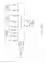


Sources:
- United States Patent and Trademark Office - verify current appl. status at the USPTO↗
Recent applications in this class:
- » 20250156587 2025-05-15
VALIDATION OF COMPONENT TRANSFERS BETWEEN INFORMATION HANDLING SYSTEMS - » 20250139299 2025-05-01
Method to Identify Consumer Electronics Products - » 20250139298 2025-05-01
OUT OF BAND COMPONENT VALIDATION - » 20250103755 2025-03-27
SYSTEMS AND METHODS FOR ESTABLISHING AND USING DEVICE IDENTITY IN INFORMATION HANDLING SYSTEMS - » 20250045463 2025-02-06
SYSTEM AND METHOD FOR NON-BYPASSABLE AND UNCLONABLE MICROELECTRONIC DEVICE FINGERPRINTING - » 20240370590 2024-11-07
SYSTEM AND METHOD FOR DETECTION OF COUNTERFEIT AND CYBER ELECTRONIC COMPONENTS - » 20240370589 2024-11-07
IDENTIFICATION KEY GENERATION CIRCUIT BASED ON PROCESS VARIATION - » 20240346185 2024-10-17
Authentication of Medical Device Computing Systems by Using Metadata Signature - » 20240311517 2024-09-19
TECHNIQUES FOR VALIDATING CLOUD REGIONS BUILT AT A PREFAB FACTORY - » 20240211639 2024-06-27
SYSTEMS AND METHODS FOR HARDWARE DEVICE FINGERPRINTING