Method of growing GaN using CVD and HVPE
US20100248461A1
2010-09-30
11/808,931
2007-06-13
✅ Patent granted
US 7,863,164 B2
2011-01-04
-
-
Alexander G Ghyka | Seahvosh J Nikmanesh
2027-06-13
Abstract:
A thick gallium nitride (GaN) film is formed on a LiAlO2 substrate through two stages. First, GaN nanorods are formed on the LiAlO2 substrate through chemical vapor deposition (CVD). Then the thick GaN film is formed through hydride vapor phase epitaxy (HVPE) by using the GaN nanorods as nucleus sites. In this way, a quantum confined stark effect (QCSE) becomes small and a problem of spreading lithium element into gaps in GaN on using the LiAlO2 substrate is mended.
Inventors:
- Wen-Ching HSU 74 🇹🇼 Hsinchu, Taiwan
- Wen-Ching HSU 21 🇹🇼 Hsinchu City, Taiwan
- Mitch M. C. Chou 5 🇹🇼 Chiayi City, Taiwan
- Mitch M. C. Chou 3 🇹🇼 Chiayi, Taiwan
Assignee:
- National Sun Yat-Sen University 52 🇹🇼 Kaohsiung City, Taiwan
- SINO-AMERICAN SILICON PRODUCTS INC. 38 🇹🇼 Hsinchu, Taiwan
- Sino American Silicon Prouducts Inc. 1 🇹🇼 Hsinchu City, Taiwan
- Natioal Sun Yat-Sen University 1 🇹🇼 Kaohsiung, Taiwan
Interested in similar patents?
Get notified when new applications in this technology area are published.
Classification:
H01L21/0242 » CPC further
Processes or apparatus adapted for the manufacture or treatment of semiconductor or solid state devices or of parts thereof; Manufacture or treatment of semiconductor devices or of parts thereof; Forming layers; Forming inorganic semiconducting materials on a substrate; Substrates; Materials Crystalline insulating materials
H01L21/02513 » CPC further
Processes or apparatus adapted for the manufacture or treatment of semiconductor or solid state devices or of parts thereof; Manufacture or treatment of semiconductor devices or of parts thereof; Forming layers; Forming inorganic semiconducting materials on a substrate; Intermediate layers between substrates and deposited layers; Structure Microstructure
H01L21/0262 » CPC further
Processes or apparatus adapted for the manufacture or treatment of semiconductor or solid state devices or of parts thereof; Manufacture or treatment of semiconductor devices or of parts thereof; Forming layers; Forming inorganic semiconducting materials on a substrate; Formation types; Deposition types Reduction or decomposition of gaseous compounds, e.g. CVD
H01L31/20 IPC
Semiconductor devices sensitive to infra-red radiation, light, electromagnetic radiation of shorter wavelength or corpuscular radiation and specially adapted either for the conversion of the energy of such radiation into electrical energy or for the control of electrical energy by such radiation; Processes or apparatus specially adapted for the manufacture or treatment thereof or of parts thereof; Details thereof; Processes or apparatus specially adapted for the manufacture or treatment of these devices or of parts thereof such devices or parts thereof comprising amorphous semiconductor materials
H01L21/20 IPC
Processes or apparatus adapted for the manufacture or treatment of semiconductor or solid state devices or of parts thereof; Manufacture or treatment of semiconductor devices or of parts thereof the devices having at least one potential-jump barrier or surface barrier, e.g. PN junction, depletion layer or carrier concentration layer the devices having semiconductor bodies comprising elements of Group IV of the Periodic System or AB compounds with or without impurities, e.g. doping materials Deposition of semiconductor materials on a substrate, e.g. epitaxial growth solid phase epitaxy
Description
FIELD OF THE INVENTION
The present invention relates to growing GaN; more particularly, relates to growing a thick GaN film on a GaN nucleus sites through a chemical vapor deposition (CVD) and a hydride vapor phase epitaxy (HVPE).
DESCRIPTION OF THE RELATED ART
An environment for growing GaN through CVD and HVPE usually uses a lot of ammonia (NH3) gas and hydrogen chloride (HCL) gas. And the HCl gas usually etches more surface than the NH3 gas.
However, the growing procedure is complex and the GaN obtained is too thin. If GaN is grown directly under HVPE by using a LiAlO2 substrate under a high temperature, a possible problem is that the lithium element in the substrate may be spread on a surface of the substrate before GaN nucleus sites are formed and thus a pollution may occur.
Consequently, the GaN obtained through the prior art may have HCl accumulated and lithium element spread into GaN structure, not to mention that the GaN obtained is too thin. Hence, the prior art does not fulfill all users' requests on actual use.
SUMMARY OF THE INVENTION
The main purpose of the present invention is to grow GaN nanostructure through a CVD and growing a thick GaN film through a HVPE on the GaN nanostructure as nucleus sites.
Another purpose of the present invention is to effectively mend a problem of spreading lithium element into gaps in GaN while using a LiAlO2 substrate.
To achieve the above purposes, the present invention is a method of growing GaN using CVD and HVPE, comprising steps of: (a) obtaining a LiAlO2 substrate and a two-stage reactor device; (b) obtaining GaN nanorods through CVD in the reactor device under a high temperature; and (c) obtaining a thick GaN film through HVPE in the reactor device with the GaN nanorods as nucleus sites. Accordingly, a novel method of growing GaN using CVD and HVPE is obtained.
BRIEF DESCRIPTIONS OF THE DRAWINGS
The present invention will be better understood from the following detailed description of the preferred embodiment according to the present invention, taken in conjunction with the accompanying drawings, in which
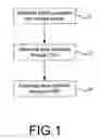
FIG. 1 is the flow view showing the preferred embodiment according to the present invention;
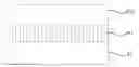
FIG. 2 is the view showing the LiAlO2 substrate;
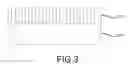
FIG. 3 is the view showing the GaN nanorods; and
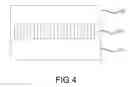
FIG. 4 is the view showing the thick GaN film
DESCRIPTION OF THE PREFERRED EMBODIMENT
The following description of the preferred embodiment is provided to understand the features and the structures of the present invention.
Please refer to FIG. 1 to FIG. 4, which are a flow view showing a preferred embodiment; a view showing a LiAlO2 substrate; a view showing a GaN nanorods; and a view showing a thick GaN film according to the present invention. As shown in the figures, the present invention is a method of growing GaN using CVD and HVPE, comprising the following steps:
(a) Obtaining a LiAlO2 substrate and a reactor device 11: As shown in FIG. 2, a LiAlO2 substrate 21 and a reactor device (not shown in the figures) are obtained. The substrate made of LiAlO2 can be further a substrate made of sapphire (Al2O3), lithium gallium oxide (LiGaO2), lithium silicon oxide (Li2SiO3), lithium germanium oxide (LiGeO3), sodium aluminum oxide (NaAlO2), sodium germanium oxide (Na2GeO3), sodium silicon oxide (Na2SiO3), lithium phosphor oxide (Li3PO4), lithium arsenic oxide (Li3AsO4), lithium vanadium oxide (Li3VO4), lithium magnesium germanium oxide (Li2MgGeO4), lithium zinc germanium oxide (Li2ZnGeO4), lithium cadmium germanium oxide (Li2CdGeO4), lithium magnesium silicon oxide (Li2MgSiO4), lithium zinc silicon oxide (Li2ZnSiO4), lithium cadmium silicon oxide (Li2CdSiO4), sodium magnesium germanium oxide (Na2MgGeO4), sodium zinc germanium oxide (Na2ZnGeO4) or sodium zinc silicon oxide (Na2ZnSiO4). The reactor device is a two-stage reactor device serially processing a CVD and an HVPE.
(b) Obtaining GaN nanorods through CVD 12: As shown in FIG. 3, the LiAlO2 substrate 21 deposed on a seat (not shown in the figure) is sent into the reactor device to be processed with the CVD. Under a high temperature, an ammonia (NH3) gas and a gallium (Ga) metal are obtained as sources for nitrogen (N) element and Ga element. A N2 gas is flowed as a carrying gas. The Ga metal is deposed in a movable boat. Then the NH3 gas is directed in a quartz tube (not shown in the figures) to pass through a mass flow controller (not shown in the figures) for processing the CVD with a chemical reaction to obtain a GaN nanostructure of nanorods 211.
(c) Obtaining a thick GaN film through HVPE 13: As shown in FIG. 4, the LiAlO2 substrate 21 having the GaN nanorods 211 is processed with the HVPE in the two-stage reactor device. A nitrogen gas is used as a diluent gas. The Ga metal and a HCl flowed into the two-stage reactor device are reacted under a temperature between 750 and 800 Celsius degrees (° C.) to obtain gallium chloride (GaCl). Then the GaN nanorods 211 are used as nucleus site where GaCl and NH3 are mixed for reaction under a temperature between 500 and 600° C. to form a thin GaN film 212 on the LiAlO2 substrate 21. Then a temperature and a speed of the gases flowed in are adjusted for growing a thick GaN film. Thus, a novel method of growing GaN using CVD and HVPE is obtained.
On using the present invention, a Ga metal is put in a movable boat with a LiAlO2 substrate 21 on a seat. The LiAlO2 substrate 21 is processed with a CVD under a high temperature in a reactor device to grow GaN nanorods 211. Therein, a linear boron nitride (BN) tube is used to prevent a quartz tube of the reactor device from pollution and to reduce an interfacial free energy between the GaN nanorods 211 and the LiAlO2 substrate 21. Thus, GaN nanorods 211 are obtained through the follow chemical formula:
2Ga+2NH3→2GaN+3H2
Then the GaN nanorods 211 are used as nucleus sites to process the HVPE in the reactor device to directly grow GaN on the nucleus sites through the following formulas:
2Ga+2HCl⇄2GaCl+H2
GaCl+NH3⇄GaN+HCl+H2
And then the LiAlO2 substrate 21 is transferred to a preheated place to be slowly cooled down in a room temperature. By adjusting a temperature of the LiAlO2 substrate and by controlling a growing condition through a small temperature difference between the LiAlO2 substrate 21 and its surrounding environment, a thick GaN film is finally obtained. And, owing to a weaker piezoelectric field of the two-stage reactor device, a quantum confined stark effect (QCSE) becomes smaller to effectively mend a problem of spreading lithium element into gaps in GaN while using a LiAlO2 substrate.
To sum up, the present invention is a method of growing GaN using CVD and HVPE, where a CVD is used to grow a GaN nanostructure and then an HVPE is used to grow a thick GaN film on the GaN nanostructure as nucleus sites; and a problem of spreading lithium element into gaps in GaN while using a LiAlO2 substrate is effectively mended.
The preferred embodiment herein disclosed is not intended to unnecessarily limit the scope of the invention. Therefore, simple modifications or variations belonging to the equivalent of the scope of the claims and the instructions disclosed herein for a patent are all within the scope of the present invention.
Claims
What is claimed is:1. A method of growing gallium nitride (GaN) using a chemical vapor deposition (CVD) and a hydride vapor phase epitaxy (HVPE), comprising steps of:
(a) obtaining a substrate made of LiAlO2 and a reactor device;
(b) deposing said LiAlO2 substrate on a seat, deposing a gallium (Ga) metal in a movable boat, flowing at least a gas into said reactor device, and processing said CVD in said reactor device under a high temperature to deposit a GaN nanostructure on said LiAlO2 substrate; and
(c) processing said LiAlO2 substrate through said HVPE in said reactor device with said GaN having said nanostructure as nucleus sites to obtain a thick GaN film by adjusting a temperature and a flow speed of said gas.
2. The method according to claim 1, wherein said reactor device is a two-stage reactor device serially processing said CVD and said HVPE.
3. The method according to claim 1, wherein said method has a device comprising:
a reactor device, said reactor device being a two-stage reactor device serially processing a CVD and an HVPE;
a substrate, said substrate having a GaN nanostructure grown on said substrate, said GaN nanostructure having a thick GaN film grown on said GaN nanostructure;
a boat, said boat being movable, said boat being deposed with a Ga metal; and
a seat, said seat being deposed with said substrate.
4. The method according to claim 1, wherein said substrate is further made of a material selected from a group consisting of sapphire (Al2O3) lithium gallium oxide (LiGaO2), lithium silicon oxide (Li2SiO3), lithium germanium oxide (LiGeO3), sodium aluminum oxide (NaAlO2) sodium germanium oxide (Na2GeO3), sodium silicon oxide (Na2SiO3), lithium phosphor oxide (Li3PO4), lithium arsenic oxide (Li3AsO4), lithium vanadium oxide (Li3VO4), lithium magnesium germanium oxide (Li2MgGeO4), lithium zinc germanium oxide (Li2ZnGeO4), lithium cadmium germanium oxide (Li2CdGeO4), lithium magnesium silicon oxide (Li2MgSiO4), lithium zinc silicon oxide (Li2ZnSiO4), lithium cadmium silicon oxide (Li2CdSiO4), sodium magnesium germanium oxide (Na2MgGeO4), sodium zinc germanium oxide (Na2ZnGeO4) and sodium zinc silicon oxide (Na2ZnSiO4).
5. The method according to claim 1, wherein said GaN nanostructure is a GaN nanorods.
Images & Drawings included:

Sources:
- United States Patent and Trademark Office - verify current appl. status at the USPTO↗
Recent applications in this class:
- » 20250293025 2025-09-18
METHOD FOR MANUFACTURING GROUP III NITRIDE SEMICONDUCTOR TEMPLATE AND SEMICONDUCTOR TEMPLATE MANUFACTURED THEREBY - » 20250285860 2025-09-11
METHOD FOR MANUFACTURING SEMICONDUCTOR TEMPLATE HAVING GROUP III METAL POLAR SURFACE - » 20250285859 2025-09-11
METHOD FOR MANUFACTURING GROUP 3 NITRIDE SEMICONDUCTOR TEMPLATE - » 20250253149 2025-08-07
METHOD OF FORMING BORON NITRIDE FILM AND FILM FORMING APPARATUS - » 20250201554 2025-06-19
MULTILAYER STRUCTURE, METHOD FOR PRODUCING MULTILAYER STRUCTURE AND SEMICONDUCTOR DEVICE - » 20250191914 2025-06-12
MULTILAYERED STRUCTURE, SEMICONDUCTOR DEVICE, AND MANUFACTURING METHOD THEREOF - » 20250118552 2025-04-10
METHOD FOR PRODUCING A CONTINUOUS NITRIDE LAYER - » 20250054754 2025-02-13
PRODUCTION METHOD FOR NITRIDE CRYSTAL SUBSTRATE, AND PEELED INTERMEDIATE - » 20250029835 2025-01-23
INTEGRATED PLASMA CLEAN AND DIELECTRIC PASSIVATION DEPOSITION PROCESSES - » 20240429050 2024-12-26
PRODUCTION METHOD FOR SEMICONDUCTOR DEVICE
Recent applications for this Assignee:
- » 20250235498 2025-07-24
METHODS OF TREATING OR PREVENTING RESPIRATORY DISEASE WITH HOUTTUYNIA CORDATA THUNB-BASED AEROSOL INHALATION THERAPY - » 20250067321 2025-02-27
CONJUGATE CAM REDUCER - » 20240354599 2024-10-24
METHOD FOR DETERMINING PROBABILITY OF A KIDNEY STONE IN A SUBJECT BEING A URIC-ACID STONE - » 20240352097 2024-10-24
NEUTRALIZING ANTIBODY FOR FLAVIVIRUSES AND PRODUCTION METHOD THEREOF - » 20240026957 2024-01-25
CONJUGATE CAM REDUCER - » 20210239446 2021-08-05
Automatic nut internal thread quality tester - » 20210237182 2021-08-05
Automatic nut tapping equipment - » 20200398304 2020-12-24
Crucible structure and method for forming isolating layer of crucible - » 20190096987 2019-03-28
N-type polysilicon crystal, manufacturing method thereof, and N-type polysilicon wafer - » 20190035946 2019-01-31
SOLAR CELL WAFER