Method for making multi-crystalline film of solar cell
US20100261305A1
2010-10-14
11/980,769
2007-10-31
✅ Patent granted
US 7,892,953 B2
2011-02-22
-
-
Charles D Garber | Andre′ C Stevenson
2027-10-31
Abstract:
A method is disclosed to make a multi-crystalline silicon film of a solar cell. The method includes the step of providing a ceramic substrate, the step of providing a titanium-based film on the ceramic substrate, the step of providing a p+-type back surface field layer on the titanium-based film, the step of providing a p−-type light-soaking layer on the p+-type back surface field layer and the step of conducting n+-type diffusive deposition of phosphine on the p−-type light-soaking layer based on atmospheric pressure chemical vapor deposition, thus forming an n+-type emitter on the p−-type light-soaking layer.
Inventors:
- Tsun-Neng Yang 35 🇹🇼 Taipei City, Taiwan
- Chin-Chen Chiang 10 🇹🇼 Taoyuan County, Taiwan
- Tsun-Neng Yang 28 🇹🇼 Taipei, Taiwan
- Shan-Ming Lan 12 🇹🇼 Daxi Town, Taiwan
- Chin-Chen Chiang 6 🇹🇼 Daxi Town, Taiwan
- Wei-Yang Ma 8 🇹🇼 Banqiao City, Taiwan
- Chien-Te Ku 10 🇹🇼 Pingzhen City, Taiwan
- Yu-Hsiang Huang 8 🇹🇼 Pingzhen City, Taiwan
- Shan-Ming Lan 15 🇹🇼 Taoyuan County, Taiwan
- Wei-Yang Ma 6 🇹🇼 Taipei County, Taiwan
- Chien-Te Ku 7 🇹🇼 Taoyuan County, Taiwan
- Yu-Hsiang Huang 4 🇹🇼 Taoyuan County, Taiwan
Assignee:
- ATOMIC ENERGY COUNCIL- INSTITUTE OF NUCLEAR ENERGY RESEARCH 159 🇹🇼 Taoyuan, Taiwan
Interested in similar patents?
Get notified when new applications in this technology area are published.
Classification:
H01L31/03682 » CPC main
Semiconductor devices sensitive to infra-red radiation, light, electromagnetic radiation of shorter wavelength or corpuscular radiation and specially adapted either for the conversion of the energy of such radiation into electrical energy or for the control of electrical energy by such radiation; Processes or apparatus specially adapted for the manufacture or treatment thereof or of parts thereof; Details thereof characterised by their semiconductor bodies characterised by their crystalline structure or particular orientation of the crystalline planes including polycrystalline semiconductors including only elements of Group IV of the Periodic System
H01L31/068 » CPC further
Semiconductor devices sensitive to infra-red radiation, light, electromagnetic radiation of shorter wavelength or corpuscular radiation and specially adapted either for the conversion of the energy of such radiation into electrical energy or for the control of electrical energy by such radiation; Processes or apparatus specially adapted for the manufacture or treatment thereof or of parts thereof; Details thereof adapted as photovoltaic [PV] conversion devices characterised by at least one potential-jump barrier or surface barrier the potential barriers being only of the PN homojunction type, e.g. bulk silicon PN homojunction solar cells or thin film polycrystalline silicon PN homojunction solar cells
H01L31/1804 » CPC further
Semiconductor devices sensitive to infra-red radiation, light, electromagnetic radiation of shorter wavelength or corpuscular radiation and specially adapted either for the conversion of the energy of such radiation into electrical energy or for the control of electrical energy by such radiation; Processes or apparatus specially adapted for the manufacture or treatment thereof or of parts thereof; Details thereof; Processes or apparatus specially adapted for the manufacture or treatment of these devices or of parts thereof comprising only elements of Group IV of the Periodic System
H01L31/1864 » CPC further
Semiconductor devices sensitive to infra-red radiation, light, electromagnetic radiation of shorter wavelength or corpuscular radiation and specially adapted either for the conversion of the energy of such radiation into electrical energy or for the control of electrical energy by such radiation; Processes or apparatus specially adapted for the manufacture or treatment thereof or of parts thereof; Details thereof; Processes or apparatus specially adapted for the manufacture or treatment of these devices or of parts thereof; Particular post-treatment for the devices, e.g. annealing, impurity gettering, short-circuit elimination, recrystallisation Annealing
Y02E10/546 » CPC further
Energy generation through renewable energy sources; Photovoltaic [PV] energy Polycrystalline silicon PV cells
Y02E10/546 » CPC further
Energy generation through renewable energy sources; Photovoltaic [PV] energy Polycrystalline silicon PV cells
Y02E10/547 » CPC further
Energy generation through renewable energy sources; Photovoltaic [PV] energy Monocrystalline silicon PV cells
Y02E10/547 » CPC further
Energy generation through renewable energy sources; Photovoltaic [PV] energy Monocrystalline silicon PV cells
Y02P70/50 » CPC further
Climate change mitigation technologies in the production process for final industrial or consumer products Manufacturing or production processes characterised by the final manufactured product
Y02P70/50 » CPC further
Climate change mitigation technologies in the production process for final industrial or consumer products Manufacturing or production processes characterised by the final manufactured product
H01L31/18 IPC
Semiconductor devices sensitive to infra-red radiation, light, electromagnetic radiation of shorter wavelength or corpuscular radiation and specially adapted either for the conversion of the energy of such radiation into electrical energy or for the control of electrical energy by such radiation; Processes or apparatus specially adapted for the manufacture or treatment thereof or of parts thereof; Details thereof Processes or apparatus specially adapted for the manufacture or treatment of these devices or of parts thereof
H01L21/20 IPC
Processes or apparatus adapted for the manufacture or treatment of semiconductor or solid state devices or of parts thereof; Manufacture or treatment of semiconductor devices or of parts thereof the devices having at least one potential-jump barrier or surface barrier, e.g. PN junction, depletion layer or carrier concentration layer the devices having semiconductor bodies comprising elements of Group IV of the Periodic System or AB compounds with or without impurities, e.g. doping materials Deposition of semiconductor materials on a substrate, e.g. epitaxial growth solid phase epitaxy
Description
FIELD OF THE INVENTION
The present invention relates to a solar cell and, more particularly, to a method for making a multi-crystalline silicon film of a solar cell.
DESCRIPTION OF THE RELATED ART
Most silicon-based solar cells are made in low-temperature processes based on plasma-enhanced chemical vapor deposition (“PECVD”). An amorphous silicon or multi-crystalline silicon film is coated on a glass, aluminum, silicon, stainless steel or plastic substrate. A back contact is made of aluminum, gold, silver or transparent conductive oxide such as indium-tin oxide (“ITO”) and zinc oxide.
The primary advantage of the low-temperature processes is the wide variety of materials that can be used to make the substrates. However, they suffer drawbacks such as defective silicon films, low photoelectrical conversion efficiencies and low light-soaking stability.
In the PECVD, while coating the microcrystalline silicon film, a silicon material is highly diluted in hydrogen. For example, [H2]/[SiH4]>15. That is, the concentration or flow rate of H2 is more than 15 times as high as that of SiH4. The problems with the PECVD are a low growth rate of the film, a long process and a high cost.
Regarding the making of the poly-silicon solar cells, there are various techniques such as solid phase crystallization (“SPC”) and aluminum-induced crystallization (“AIC”). The SPC is based on the PECVD. An amorphous silicon film is deposited, intensively heated and annealed at a high temperature. Thus, a poly-silicon film with a grain size of 1 to 2 micrometers is made.
In the AIC as shown in FIGS. 5 through 9, an aluminum film 32 is coated on a substrate 31. An amorphous silicon film 33 is coated on the aluminum film 32 based on the PECVD and annealed at a temperature of about 575 degrees Celsius for a long time to form a seeding layer 34. Then, it is subjected to an epitaxial process such as the PECVD or an electron cyclotron resonance chemical deposition (“ECR-CVD”) to make a poly-silicon film 35. The AIC however involves many steps and takes a long time. The resultant grain size is about 0.1 to 10 micrometers.
As discussed above, regarding the conventional methods for making poly-silicon film solar cells in the low-temperature processes based on the PECVD, there are many defects in the silicon films, the photoelectrical conversion efficiencies are low, the light soaking stabilities low, the growth rates of the films low, the processes long, and the costs high. Concerning the method for making poly-silicon film solar cells based on the AIC, the processes are long for including many steps and therefore expensive.
The present invention is therefore intended to obviate or at least alleviate the problems encountered in prior art.
SUMMARY OF THE INVENTION
It is an objective of the present invention is to provide an efficient method for making a multi-crystalline silicon film of a solar cell.
It is another objective of the present invention to provide a method for providing a quality multi-crystalline silicon film of a solar cell.
It is another objective of the present invention to provide a method for making a multi-crystalline silicon film that can be used to make a solar cell that exhibits a high photoelectrical conversion efficiency and stability of the soaking of light.
To achieve the fore-going objectives, the method includes the step of providing a ceramic substrate, the step of providing a titanium-based film on the ceramic substrate, the step of providing a p+-type back surface field layer on the titanium-based film, the step of providing a p−-type light-soaking layer on the p+-type back surface field layer and the step of conducting n+-type diffusive deposition of phosphine on the p−-type light-soaking layer based on atmospheric pressure chemical vapor deposition, thus forming an n+-type emitter on the p−-type light-soaking layer.
Other objectives, advantages and features of the present invention will become apparent from the following description referring to the attached drawings.
BRIEF DESCRIPTIONS OF THE DRAWINGS
The present invention will be described via the detailed illustration of the preferred embodiment referring to the drawings.
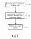
FIG. 1 is a flowchart of a method for making a multi-crystalline silicon film of a solar cell according to the preferred embodiment of the present invention.
FIG. 2 is a side view of a ceramic substrate, a titanium-based film coated on the ceramic substrate, a p+-type back surface field layer coated on the titanium-based film and a p−-type light-soaking layer coated on the p+-type back surface field layer in the method shown in FIG. 1.
FIG. 3 is a side view of an atmospheric pressure chemical vapor deposition device for diffusively depositing phosphine on the p−-type light-soaking layer shown in FIG. 2.
FIG. 4 is a side view of an n+-type emitter coated on the p−-type light-soaking layer shown in FIG. 3.
FIG. 5 is a side view of a substrate used in a conventional method for making a multi-crystalline silicon film.
FIG. 6 is a side view of an aluminum film coated on the substrate shown in FIG. 5.
FIG. 7 is a side view of an amorphous silicon film coated on the aluminum film shown in FIG. 6.
FIG. 8 is a side view of the substrate coated with a seed layer converted from the amorphous silicon film and the aluminum film shown in FIG. 7.
FIG. 9 is a side view of a multi-crystalline silicon film coated on the seed layer shown in FIG. 6.
DESCRIPTIONS OF THE PREFERRED EMBODIMENTS
Referring to FIG. 1, shown is a method for making a multi-crystalline silicon film of a solar cell according to the preferred embodiment of the present invention.
Referring to FIGS. 1 and 2, at 11, a ceramic substrate 21 is provided. The ceramic substrate 21 is made of aluminum oxide. The thickness of the substrate 21 is about 0.1 to 1.0 mm.
A titanium-based film 22 is coated on the ceramic substrate 21. The thickness of the titanium-based film 22 is about 1000 to 5000 angstroms. The titanium-based film 22 is used both as a back contact and a seed layer. The titanium-based film 22 is made of TiSi2, TiN, TiC, TiB2 or TiCxNy.
The epitaxial growth of a p+-type back surface field (“BSF”) layer 23 is conducted on the titanium-based film 22. The thickness of the p+-type BSF layer 23 is no larger than 1 micrometer.
The epitaxial growth of a p−-type light-soaking layer 24 is conducted on the p+-type BSF layer 23. The thickness of the p−-type light-soaking layer 24 is about 15 micrometers. The size of silicon crystals 241 at grain boundaries 242 in the p−-type light-soaking layer 24 is larger than 10 micrometers.
Referring to FIGS. 1 and 3, at 12, in an atmospheric pressure chemical vapor deposition (“APCVD”) device 3, at about 800 to 1000 degrees Celsius, phosphine is diffusively deposited on the p−-type light-soaking layer 24. Thus, the n+-type diffusive deposition of the phosphorous atoms of the phosphine is conducted on the p−-type light-soaking layer 24.
Referring to FIGS. 1 and 4, at 13, an n+-type emitter 25 is coated on the p−-type light-soaking layer 24. The thickness of the n+-type emitter 25 is smaller than 1000 angstroms. The concentration of the phosphorous atoms in the n+-type emitter 25 is about 1018 to 1019 #/mm3.
As discussed above, the atmospheric pressure chemical vapor deposition process is conducted at a high temperature. The ceramic substrate 21 is made of aluminum oxide. The titanium-based film 22 is used both as the back contact and the seed layer. The epitaxial growth of the P+-type BSF layer 23 and the p−-type light-soaking layer 24 is directly conducted on the titanium-based film 22. The n+-type diffusive deposition is conducted on the p−-type light-soaking layer 24. Thus, the n+-type emitter 25 thinner than 1000 angstroms is formed. Moreover, as multi-crystalline silicon exhibits high electron-hole mobility, large electron-hole diffusion length and long electron-hole recombination, the solar cell made according to the present invention exhibits a high epitaxial growth rate, excellent crystal quality, a high photoelectrical conversion efficiency and stable light-soaking. In addition, the cost of equipment is low, and the process simple.
The present invention has been described via the detailed illustration of the preferred embodiment. Those skilled in the art can derive variations from the preferred embodiment without departing from the scope of the present invention. Therefore, the preferred embodiment shall not limit the scope of the present invention defined in the claims.
Claims
What is claimed is:1. A method for making a multi-crystalline silicon film of a solar cell, the method comprising the steps of:
providing a ceramic substrate;
providing a titanium-based film on the ceramic substrate;
providing a p+-type back surface field layer on the titanium-based film;
providing a p−-type light-soaking layer on the p+-type back surface field layer; and
conducting n+-type diffusive deposition of phosphine on the p−-type light-soaking layer based on atmospheric pressure chemical vapor deposition, thus forming an n+-type emitter on the p−-type light-soaking layer.
2. The method according to claim 1, wherein the titanium-based film is made of a material selected from a group consisting of TiSi2, TiN, TiC, TiB2 and TiCxNy.
3. The method according to claim 1, wherein the thickness of the titanium-based film is about 1000 to 5000 angstroms.
4. The method according to claim 1, wherein the titanium-based film is used both as a back contact and a seed layer.
5. The method according to claim 1, wherein the thickness of the ceramic substrate is about 0.1 to 1.0 mm.
6. The method according to claim 1, wherein the thickness of the p+-type back surface field layer is no larger than 1 micrometer.
7. The method according to claim 1, wherein the thickness of the p−-type light-soaking layer is about 1 to 15 micrometers, and the grain size of the p−-type light-soaking layer is larger than 10 micrometers.
8. The method according to claim 1, wherein the n+-type diffusive deposition is conducted at 800 to 1000 degrees Celsius.
9. The method according to claim 1, wherein the thickness of the n+-type emitter is smaller than 1000 angstroms.
10. The method according to claim 1, wherein the concentration of the phosphorous atoms in the n+-type emitter is about 1018 to 1019 #/mm3.
Images & Drawings included:


Sources:
- United States Patent and Trademark Office - verify current appl. status at the USPTO↗
Recent applications in this class:
- » 20240234602 2024-07-11
CONDUCTIVE PASTE COMPOSITION, PREPARATION METHOD AND USE THEREOF, CRYSTALLINE SILICON SOLAR CELL - » 20240105870 2024-03-28
PHOTODETECTION ELEMENT AND METHOD FOR MANUFACTURING PHOTODETECTION ELEMENT - » 20240063318 2024-02-22
CRYSTALLINE SILICON SOLAR CELL AND METALLIZATION METHOD THEREFOR - » 20170062635 2017-03-02
Polycrystalline silicon column and polycrystalline silicon wafer - » 20170018667 2017-01-19
Thick damage buffer for foil-based metallization of solar cells - » 20160155868 2016-06-02
CRYSTALLINE SILICON SOLAR CELL AND METHOD FOR PRODUCING SAME - » 20150280031 2015-10-01
Solar cells with tunnel dielectrics - » 20150122321 2015-05-07
SOLAR CELL - » 20140134788 2014-05-15
Method of fabricating a solar cell with a tunnel dielectric layer - » 20140124019 2014-05-08
LOW VACUUM FABRICATION OF MICROCRYSTALLINE SOLAR CELLS
Recent applications for this Assignee:
- » 20160028091 2016-01-28
Method for manufacturing solid oxide fuel cell anode with high stability and high efficiency - » 20120279945 2012-11-08
Direct current steam plasma torch and method for reducing the erosion of electrodes thereof - » 20120070938 2012-03-22
Method of fabricating silicon nanowire solar cell device having upgraded metallurgical grade silicon substrate - » 20110251056 2011-10-13
Method of fabricating layered nano-carbonate used for medium-high temperature COsorbent - » 20110139020 2011-06-16
Apparatus for restraining a squeezed CRD blade - » 20110108429 2011-05-12
Method of recycling Cd-112 isotope - » 20110091991 2011-04-21
Protein Biomarkers for Alzheimer's Disease Detection - » 20110082679 2011-04-07
Apparatus of simulating data certification with safe network communication - » 20110062946 2011-03-17
Eddy current probes having magnetic gap - » 20110060582 2011-03-10
Diversity and defense-in-depth simulation apparatus