Solar Cell Device Having Low Electrical and Thermal Impedance
US20100282311A1
2010-11-11
12/637,424
2009-12-14
Abstract:
A solar cell is fabricated. Its light-absorbing part is close to a heat-diffusing device. Thus, the solar cell has low electrical and thermal Impedance. The solar cell has a strong structure, high efficiency and is fit for mass production.
Assignee:
- ATOMIC ENERGEY COUNCIL-INSTITUTE OF NUCLEAR ENERGY RESEARCH 1 🇹🇼 Lungtan, Taiwan
Interested in similar patents?
Get notified when new applications in this technology area are published.
Classification:
H01L31/052 » CPC main
Semiconductor devices sensitive to infra-red radiation, light, electromagnetic radiation of shorter wavelength or corpuscular radiation and specially adapted either for the conversion of the energy of such radiation into electrical energy or for the control of electrical energy by such radiation; Processes or apparatus specially adapted for the manufacture or treatment thereof or of parts thereof; Details thereof adapted as photovoltaic [PV] conversion devices Cooling means directly associated or integrated with the PV cell, e.g. integrated Peltier elements for active cooling or heat sinks directly associated with the PV cells
H01L31/035281 » CPC further
Semiconductor devices sensitive to infra-red radiation, light, electromagnetic radiation of shorter wavelength or corpuscular radiation and specially adapted either for the conversion of the energy of such radiation into electrical energy or for the control of electrical energy by such radiation; Processes or apparatus specially adapted for the manufacture or treatment thereof or of parts thereof; Details thereof characterised by their semiconductor bodies characterised by their shape or by the shapes, relative sizes or disposition of the semiconductor regions characterised by at least one potential jump barrier or surface barrier Shape of the body
H01L31/06 » CPC further
Semiconductor devices sensitive to infra-red radiation, light, electromagnetic radiation of shorter wavelength or corpuscular radiation and specially adapted either for the conversion of the energy of such radiation into electrical energy or for the control of electrical energy by such radiation; Processes or apparatus specially adapted for the manufacture or treatment thereof or of parts thereof; Details thereof adapted as photovoltaic [PV] conversion devices characterised by at least one potential-jump barrier or surface barrier
Y02E10/50 » CPC further
Energy generation through renewable energy sources Photovoltaic [PV] energy
Y02E10/50 » CPC further
Energy generation through renewable energy sources Photovoltaic [PV] energy
H01L31/02 IPC
Semiconductor devices sensitive to infra-red radiation, light, electromagnetic radiation of shorter wavelength or corpuscular radiation and specially adapted either for the conversion of the energy of such radiation into electrical energy or for the control of electrical energy by such radiation; Processes or apparatus specially adapted for the manufacture or treatment thereof or of parts thereof; Details thereof Details
Description
FIELD OF THE INVENTION
The present invention relates to a solar cell device; more particularly, relates to adhering a light absorption region to a heat dissipation device for reducing an electric resistance and a thermal resistance with strong structure and high efficiency.
DESCRIPTION OF THE RELATED ARTS
A general solar cell device, as shown in FIG. 5, comprises a thin substrate 4 and a plurality of electric contact pads 5 deposed above the substrate 4, where the solar cell device can be adhered to a heat dissipation device 7 by using a bonding agent on a lower flat surface of the substrate 4.
However, the above structure requires a complex procedure. For example, since the substrate 4 is weak during wire bonding on wafer, an extra substrate is needed for bonding; but the same extra substrate is removed later. As a result, the fabricating time is prolonged and is not good for mass production. In addition, the whole structure does not have enough heat dissipation efficiency. Hence, when the device is used under a high condensing light, heat is greatly aggregated and so the device is reduced in efficiency and even in life of use. Hence, the prior art does not fulfill all users' requests on actual use.
SUMMARY OF THE INVENTION
The main purpose of the present invention is to adhere a light absorption region of a solar cell to a heat dissipation device for reducing an electric resistance and a thermal resistance with strong structure and high efficiency.
To achieve the above purpose, the present invention is a solar cell device having low electrical and thermal impedance, comprising a substrate, a plurality of electric contact pads and an ohmic contact, where the substrate has an upper surface and a lower surface; the lower surface is corresponding to the upper surface; the substrate has a recessed hole on the lower surface; the recessed hole has openings connected with four recessed channels; the recessed hole comprises a central recess and a recess sidewall; the recess sidewall surrounds the central recess; the electric contact pads is deposed on the upper surface of the substrate; and the ohmic contact is deposed on the lower surface, the recessed hole and the recessed channels. Accordingly, a novel solar cell device having low electrical and thermal impedance is obtained.
BRIEF DESCRIPTIONS OF THE DRAWINGS
The present invention will be better understood from the following detailed description of the preferred embodiment according to the present invention, taken in conjunction with the accompanying drawings, in which
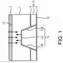
FIG. 1 is the sectional side view showing the preferred embodiment according to the present invention;
FIG. 2 to FIG. 4 are the first to the third sectional bottom-up views showing the preferred embodiment; and
FIG. 5 is the view of the prior art.
DESCRIPTION OF THE PREFERRED EMBODIMENT
The following description of the preferred embodiment is provided to understand the features and the structures of the present invention.
Please refer to FIG. 1, which is a sectional side view showing a preferred embodiment according to the present invention. As shown in the figure, the preferred embodiment is a solar cell device having low electrical and thermal impedance, comprising a substrate 1, a plurality of electric contact pads 2 and an ohmic contact 3.
The substrate 1 has an upper surface 11 and a lower surface 12; the lower surface 12 is corresponding to the upper surface 11; the lower surface 12 has a columnar recessed hole 13 and four recessed channels 14˜17 connected with openings of the recessed hole 13; the recessed channel 13 is made of an electric and thermal conductive material; the recessed hole 13 comprises a central recess 131 and a recess sidewall 132 surrounding the central recess 131; and, every one of the recessed channels 14˜17 has a depth not deeper than that of the recessed hole 13.
The electric contact pads 2 are deposed on at least a part of the upper surface 11.
The ohmic contact 3 is deposed on the lower surface 12, the recessed hole 13 and the recessed channels 14˜17. Thus, a novel solar cell device having low electrical and thermal impedance is obtained.
Please refer to FIG. 2 to FIG. 4, which are a first to a third sectional bottom-up views showing the preferred embodiment. As shown in the figures, on using the present invention, a recessed hole 13 is a square hole (in FIG. 2) or a circular hole (in FIG. 3); and recessed channels 14˜17 connected with openings of the recessed hole 13 are two channels (14,15 or 16,17) or three channels 14˜16 (in FIG. 4).
A light absorption region of the present invention is thus adhered to a heat dissipation device. Hence, an electric resistance and a thermal resistance are greatly reduced when the light absorption region is bonded to the recessed channels. Furthermore, the present invention has a strong structure and do not need extra bonding substrate while photon is reflected at back of the device; so more current is outputted efficiently and the present invention can be easily fabricated for mass production.
To sum up, the present invention is a solar cell device having low electrical and thermal impedance, where a light absorption region of the solar cell device is adhered to a heat dissipation device for reducing an electric resistance and a thermal resistance with a strong structure and a high efficiency; and the present invention can be easily fabricated for mass production.
The preferred embodiment herein disclosed is not intended to unnecessarily limit the scope of the invention. Therefore, simple modifications or variations belonging to the equivalent of the scope of the claims and the instructions disclosed herein for a patent are all within the scope of the present invention.
Claims
What is claimed is:1. A solar cell device having low electrical and thermal impedance, comprising
a substrate, said substrate having an upper surface and a lower surface, said lower surface being corresponding to said upper surface, said substrate having a recessed hole on said lower surface, said recessed hole having openings connected with four recessed channels, said recessed hole comprising a central recess and a recess sidewall, said recess sidewall surrounding said central recess;
a plurality of electric contact pads, said electric contact pads being deposed on said upper surface of said substrate; and
an ohmic contact, said ohmic contact being deposed on said lower surface, said recessed hole and said recessed channels.
2. The solar cell device according to claim 1, wherein said recessed hole is a square hole.
3. The solar cell device according to claim 1, wherein said recessed hole is a circular hole.
4. The solar cell device according to claim 1, wherein said recessed channel is made of an electric and thermal conductive material.
5. The solar cell device according to claim 1, wherein said recessed hole has openings connected with two recessed channels.
6. The solar cell device according to claim 1, wherein said recessed hole has openings connected with three recessed channels.
7. The solar cell device according to claim 1, wherein said recessed channel has a depth not deeper than that of said recessed hole.
Images & Drawings included:


Sources:
- United States Patent and Trademark Office - verify current appl. status at the USPTO↗
Recent applications in this class:
- » 20250072162 2025-02-27
HORIZONTAL BALANCED SOLAR TRACKER - » 20250063852 2025-02-20
HORIZONTAL BALANCED SOLAR TRACKER - » 20240387760 2024-11-21
HEAT DISSIPATING STRUCTURES FOR SOLAR CELL ARRAYS FOR USE IN SPACE APPLICATIONS - » 20240234609 2024-07-11
SOLAR CELL, SOLAR CELL MODULE AND SOLAR CELL MANUFACTURING EQUIPMENT - » 20240186437 2024-06-06
Self-similar high efficiency solar cells and concentrators - » 20240136458 2024-04-25
SOLAR CELL, SOLAR CELL MODULE AND SOLAR CELL MANUFACTURING EQUIPMENT - » 20240088318 2024-03-14
HEAT CONDUCTING LAYERS FOR PHOTOVOLTAIC MODULES - » 20230275173 2023-08-31
STRUCTURES AND METHODS FOR PRODUCING AN OPTOELECTRONIC DEVICE - » 20230163227 2023-05-25
A Heat Exchanger and Uses Thereof - » 20220367742 2022-11-17
Thermal conductive and electrically insulating paint composition, and exterior steel sheet for solar cell comprising same