Thin wafer handling structure and method
US20100330788A1
2010-12-30
12/818,362
2010-06-18
✅ Patent granted
US 8,871,609 B2
2014-10-28
-
-
Calvin Choi
Lowe Hauptman & Ham, LLP
2030-06-18
Abstract:
A thin wafer handling structure includes a semiconductor wafer, a release layer that can be released by applying energy, an adhesive layer that can be removed by a solvent, and a carrier, where the release layer is applied on the carrier by coating or laminating, the adhesive layer is applied on the semiconductor wafer by coating or laminating, and the semiconductor wafer and the carrier is bonded together with the release layer and the adhesive layer in between. The method includes applying a release layer on a carrier, applying an adhesive layer on a semiconductor wafer, bonding the carrier and the semiconductor wafer, releasing the carrier by applying energy on the release layer, e.g. UV or laser, and cleaning the semiconductor's surface by a solvent to remove any residue of the adhesive layer.
Inventors:
- Ching-Wen Hsiao 14 🇹🇼 Banqiao City, Taiwan
- Chen-Shien Chen 319 🇹🇼 Zhubei City, Taiwan
- Chen-Hua YU 1,372 🇹🇼 Hsinchu, Taiwan
- Kuo-Ching HSU 31 🇹🇼 Chung-Ho City, Taiwan
- Chen-Shien Chen 311 🇹🇼 Zhubei, Taiwan
- Kuo-Ching Hsu 29 🇹🇼 Chung-Ho, Taiwan
- Ching-Wen Hsiao 12 🇹🇼 Banqiao, Taiwan
Assignee:
- TAIWAN SEMICONDUCTOR MANUFACTURING COMPANY, LTD. 15,428 🇹🇼 Hsinchu, Taiwan
- TAIWAN SEMICONDUCTOR MANUFACTURING COMPANY, LTD. 1,384 🇹🇼 , Taiwan
Applicant:
Interested in similar patents?
Get notified when new applications in this technology area are published.
Classification:
Y10T428/1476 » CPC further
Stock material or miscellaneous articles; Layer or component removable to expose adhesive Release layer
H01L21/306 IPC
Processes or apparatus adapted for the manufacture or treatment of semiconductor or solid state devices or of parts thereof; Manufacture or treatment of semiconductor devices or of parts thereof the devices having at least one potential-jump barrier or surface barrier, e.g. PN junction, depletion layer or carrier concentration layer the devices having semiconductor bodies comprising elements of Group IV of the Periodic System or AB compounds with or without impurities, e.g. doping materials; Treatment of semiconductor bodies using processes or apparatus not provided for in groups - to change their surface-physical characteristics or shape, e.g. etching, polishing, cutting Chemical or electrical treatment, e.g. electrolytic etching
H01L21/3205 IPC
Processes or apparatus adapted for the manufacture or treatment of semiconductor or solid state devices or of parts thereof; Manufacture or treatment of semiconductor devices or of parts thereof the devices having at least one potential-jump barrier or surface barrier, e.g. PN junction, depletion layer or carrier concentration layer the devices having semiconductor bodies comprising elements of Group IV of the Periodic System or AB compounds with or without impurities, e.g. doping materials; Treatment of semiconductor bodies using processes or apparatus not provided for in groups - to form insulating layers thereon, e.g. for masking or by using photolithographic techniques ; After treatment of these layers; Selection of materials for these layers Deposition of non-insulating-, e.g. conductive- or resistive-, layers on insulating layers; After-treatment of these layers
B32B7/12 IPC
Layered products characterised by the relation between layers; Layered products characterised by the relative orientation of features between layers, or by the relative values of a measurable parameter between layers, i.e. products comprising layers having different physical, chemical or physicochemical properties; Layered products characterised by the interconnection of layers; Interconnection of layers using interposed adhesives or interposed materials with bonding properties
C23C14/34 IPC
Coating by vacuum evaporation, by sputtering or by ion implantation of the coating forming material characterised by the process of coating Sputtering
B24B1/00 IPC
Processes of grinding or polishing; Use of auxiliary equipment in connection with such processes
H01L21/187 » CPC main
Processes or apparatus adapted for the manufacture or treatment of semiconductor or solid state devices or of parts thereof; Manufacture or treatment of semiconductor devices or of parts thereof the devices having at least one potential-jump barrier or surface barrier, e.g. PN junction, depletion layer or carrier concentration layer the devices having semiconductor bodies comprising elements of Group IV of the Periodic System or AB compounds with or without impurities, e.g. doping materials; Joining of semiconductor bodies for junction formation by direct bonding
H01L21/30 IPC
Processes or apparatus adapted for the manufacture or treatment of semiconductor or solid state devices or of parts thereof; Manufacture or treatment of semiconductor devices or of parts thereof the devices having at least one potential-jump barrier or surface barrier, e.g. PN junction, depletion layer or carrier concentration layer the devices having semiconductor bodies comprising elements of Group IV of the Periodic System or AB compounds with or without impurities, e.g. doping materials Treatment of semiconductor bodies using processes or apparatus not provided for in groups -
H01L21/46 IPC
Processes or apparatus adapted for the manufacture or treatment of semiconductor or solid state devices or of parts thereof; Manufacture or treatment of semiconductor devices or of parts thereof the devices having at least one potential-jump barrier or surface barrier, e.g. PN junction, depletion layer or carrier concentration layer the devices having semiconductor bodies not provided for in groups, , , and with or without impurities, e.g. doping materials Treatment of semiconductor bodies using processes or apparatus not provided for in groups
H01L21/683 IPC
Processes or apparatus adapted for the manufacture or treatment of semiconductor or solid state devices or of parts thereof; Apparatus specially adapted for handling semiconductor or electric solid state devices during manufacture or treatment thereof; Apparatus specially adapted for handling wafers during manufacture or treatment of semiconductor or electric solid state devices or components ; Apparatus not specifically provided for elsewhere for supporting or gripping
H01L21/18 IPC
Processes or apparatus adapted for the manufacture or treatment of semiconductor or solid state devices or of parts thereof; Manufacture or treatment of semiconductor devices or of parts thereof the devices having at least one potential-jump barrier or surface barrier, e.g. PN junction, depletion layer or carrier concentration layer the devices having semiconductor bodies comprising elements of Group IV of the Periodic System or AB compounds with or without impurities, e.g. doping materials
H01L21/6835 » CPC further
Processes or apparatus adapted for the manufacture or treatment of semiconductor or solid state devices or of parts thereof; Apparatus specially adapted for handling semiconductor or electric solid state devices during manufacture or treatment thereof; Apparatus specially adapted for handling wafers during manufacture or treatment of semiconductor or electric solid state devices or components ; Apparatus not specifically provided for elsewhere for supporting or gripping using temporarily an auxiliary support
H01L2221/68381 » CPC further
Processes or apparatus adapted for the manufacture or treatment of semiconductor or solid state devices or of parts thereof covered by; Apparatus for handling semiconductor or electric solid state devices during manufacture or treatment thereof; Apparatus for handling wafers during manufacture or treatment of semiconductor or electric solid state devices or components; Apparatus not specifically provided for elsewhere for supporting or gripping using temporarily an auxiliary support Details of chemical or physical process used for separating the auxiliary support from a device or wafer
H01L2221/68327 » CPC further
Processes or apparatus adapted for the manufacture or treatment of semiconductor or solid state devices or of parts thereof covered by; Apparatus for handling semiconductor or electric solid state devices during manufacture or treatment thereof; Apparatus for handling wafers during manufacture or treatment of semiconductor or electric solid state devices or components; Apparatus not specifically provided for elsewhere for supporting or gripping using temporarily an auxiliary support used during dicing or grinding
H01L2221/68318 » CPC further
Processes or apparatus adapted for the manufacture or treatment of semiconductor or solid state devices or of parts thereof covered by; Apparatus for handling semiconductor or electric solid state devices during manufacture or treatment thereof; Apparatus for handling wafers during manufacture or treatment of semiconductor or electric solid state devices or components; Apparatus not specifically provided for elsewhere for supporting or gripping using temporarily an auxiliary support Auxiliary support including means facilitating the separation of a device or wafer from the auxiliary support
H01L21/26 IPC
Processes or apparatus adapted for the manufacture or treatment of semiconductor or solid state devices or of parts thereof; Manufacture or treatment of semiconductor devices or of parts thereof the devices having at least one potential-jump barrier or surface barrier, e.g. PN junction, depletion layer or carrier concentration layer the devices having semiconductor bodies comprising elements of Group IV of the Periodic System or AB compounds with or without impurities, e.g. doping materials Bombardment with radiation
H01L21/265 IPC
Processes or apparatus adapted for the manufacture or treatment of semiconductor or solid state devices or of parts thereof; Manufacture or treatment of semiconductor devices or of parts thereof the devices having at least one potential-jump barrier or surface barrier, e.g. PN junction, depletion layer or carrier concentration layer the devices having semiconductor bodies comprising elements of Group IV of the Periodic System or AB compounds with or without impurities, e.g. doping materials; Bombardment with radiation with high-energy radiation producing ion implantation
Description
CROSS-REFERENCE TO RELATED APPLICATIONS
The present application claims priority of U.S. Provisional Patent Application Ser. No. 61/221,890 filed on Jun. 30, 2009 which is incorporated herein by reference in its entirety.
TECHNICAL FIELD
This disclosure relates generally to wafer processing and more particularly to a thin wafer handling structure and method to facilitate bonding and debonding.
BACKGROUND
In semiconductor wafer processing, temporary bonding and debonding techniques are necessary for thin wafer backside processes. The wafer is bonded on rigid carrier by adhesive layers. After grinding and/or other post-bonding processes the wafer is debonded from the rigid carrier.
One of the conventional debonding methods uses a laser on a light-to-heat conversion layer (LTHC) to release the carrier, and then peel off the adhesive. The adhesive material is UV-cured material, e.g. thermal setting polymer that cannot be stripped by chemicals and should be peeled off instead. This method suffers chemical residue after debonding. Also, the laser release layer has a weak chemical resistance during backside processes.
Another conventional method uses chemical release. This method chemically dissolves the adhesive to release the wafer from the carrier. This method needs perforated glass and easily induces cross contamination. The process speed, e.g. wafers per hour (WPH) is also slow compared to the other methods.
Yet another conventional method is thermal sliding. This method treats the wafer and carrier with heat and then slides them apart. This method needs higher debonding temperatures and may adversely impact the interconnection scheme.
Accordingly, new structure and methods are desired for a robust wafer bonding to ensure surface cleanness after debonding and to have good chemical resistance during post-bonding processes.
BRIEF DESCRIPTION OF THE DRAWINGS
For a more complete understanding of the present disclosure, and the advantages thereof, reference is now made to the following descriptions taken in conjunction with the accompanying drawings, in which:
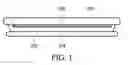
FIG. 1 illustrates an example of a thin wafer handling structure to facilitate bonding and debonding according to one aspect of the present disclosure; and
FIG. 2 illustrates an example method to facilitate thin wafer bonding and debonding according to another aspect of the present disclosure.
DETAILED DESCRIPTION OF ILLUSTRATIVE EMBODIMENTS
The making and using of the presently preferred embodiments are discussed in detail below. It should be appreciated, however, that the present disclosure provides many applicable inventive concepts that can be embodied in a wide variety of specific contexts. The specific embodiments discussed are merely illustrative of specific ways to make and use the disclosure, and do not limit the scope of the invention.
A thin wafer handling structure and method to facilitate bonding and debonding for wafer process are provided. Throughout the various views and illustrative embodiments of the present disclosure, like reference numbers are used to designate like elements.
FIG. 1 illustrates an example of a thin wafer handling structure to facilitate bonding and debonding according to one aspect of the present disclosure. The wafer 102 is bonded on the carrier 108 using two layers in between, i.e. the release layer 106 and the adhesive layer 104. The release layer 106 is applied on carrier 108 by coating or lamination processes followed by removal of the outer most 0.1 mm-3 mm of the release layer 106 from the edge of the carrier by edge bead removal (EBR).
EBR removes a build-up of material at the wafer edges. Without any intervention, excess material may accumulate at the edge of the wafer at up to several times the nominal thickness of the layer. Such a condition would present a significant contamination risk for process equipment. For chemical EBR, solvent is dispensed on the edge of the wafer as the wafer is rotated immediately after coating.
The adhesive layer 104 is applied on wafer 102 by coating or lamination process, and should be capable of being removed by solvent, e.g. thermal plastic polymer can be used as the adhesive layer 104 in one preferred embodiment. The carrier 108 and the wafer 102 are bonded together by UV light or thermal energy.
FIG. 2 illustrates an example method to facilitate thin wafer bonding and debonding according to another aspect of the present disclosure. At step 202, the release layer 106 is applied on the carrier 108 by coating or lamination. Spin coating can be used for adhesive layer application according to one embodiment. At step 204, the adhesive layer 104 is applied on the wafer 102 by coating or lamination. At step 206, the carrier 108 and the wafer 102 are bonded together with the release layer 106 and the adhesive layer 104 in between and cured by thermal energy or UV light. The adhesive can be pre-baked prior to bonding. At step 208, the wafer goes through post-bonding processes, e.g. grinding, wafer backside processing, etc. The wafer backside processing may include ion implantation, annealing, etching, sputtering, evaporation, and/or metallization, etc.
After the post-bonding processes, the wafer goes through the debonding processes, which includes carrier release and post cleaning. At step 210, the carrier 108 is released by energy application on the release layer 106, e.g. UV light or light from a laser. The thin wafer 102 can be attached on dicing frame for dicing tape lamination prior to releasing the carrier. Then the wafer 102 surface is cleaned by chemical soaking in solvent to remove any residue of the adhesive layer 104. For example, an adhesive layer 104 using thermal plastic polymer can be chemically cleaned with a solvent. A skilled person in the art will appreciate that there can be many embodiment variations of this disclosure.
The advantageous features of the present disclosure include surface cleanness after debonding and good chemical resistance during post-bonding processes. Although the present disclosure and its advantages have been described in detail, it should be understood that various changes, substitutions and alterations can be made herein without departing from the spirit and scope of the invention as defined by the appended claims. Moreover, the scope of the present application is not intended to be limited to the particular embodiments of the process, machine, manufacture, and composition of matter, means, methods and steps described in the specification. As one of ordinary skill in the art will readily appreciate from the disclosure, processes, machines, manufacture, compositions of matter, means, methods, or steps, presently existing or later to be developed, that perform substantially the same function or achieve substantially the same result as the corresponding embodiments described herein may be utilized according to the present disclosure.
Claims
What is claimed is:1. A thin wafer handling structure, comprising:
a semiconductor wafer;
a release layer that can be released by applying energy;
an adhesive layer that can be removed by a solvent; and
a carrier;
wherein the release layer is applied to the carrier by at least one of coating or laminating, the adhesive layer is applied to the semiconductor wafer by at least one of coating or laminating, and the semiconductor wafer and the carrier are bonded together with the release layer and the adhesive layer in between the semiconductor wafer and the carrier.
2. The structure of claim 1, wherein the carrier and the semiconductor wafer are bonded together by applying at least one of UV light or thermal energy.
3. The structure of claim 1, wherein the release layer goes through edge bead removal (EBR) process after the at least one of coating or laminating onto the carrier.
4. The structure of claim 3, wherein the EBR process removes the outer most 0.1 mm-3 mm of the release layer from an edge of the carrier.
5. The structure of claim 1, wherein the release layer is released by applying at least one of UV light or light from a laser.
6. The structure of claim 1, wherein the adhesive layer is thermal plastic polymer.
7. A method, comprising:
applying a release layer on a carrier by at least one of coating or lamination;
applying an adhesive layer to a semiconductor wafer by at least one of coating or lamination;
bonding the carrier and the semiconductor wafer with the release layer and the adhesive layer in between the carrier and the semiconductor wafer;
releasing the carrier by applying energy to the release layer; and
cleaning a surface of the semiconductor wafer with a solvent to remove any residue of the adhesive layer.
8. The method of claim 7, further comprising performing a post-bonding process on the semiconductor wafer.
9. The method of claim 8, wherein the post-bonding process includes grinding and/or wafer backside processing.
10. The method of claim 9, wherein the wafer backside processing includes at least one of ion implantation, annealing, etching, sputtering, evaporation or metallization.
11. The method of claim 7, wherein the carrier and the semiconductor wafer are bonded together by applying UV light or thermal energy.
12. The method of claim 7, wherein the release layer is released by applying UV light or light from a laser.
13. The method of claim 7, wherein the adhesive layer is thermal plastic polymer that can be chemically cleaned with a solvent.
14. The method of claim 7, further comprising performing edge bead removal (EBR) process on the release layer after coating or laminating onto the carrier.
15. The method of claim 14, wherein the EBR process removes the outer most 0.1 mm-3 mm.
16. A method, comprising:
applying a release layer to a carrier by at least one of coating or lamination;
applying an adhesive layer to a semiconductor wafer by at least one of coating or lamination;
bonding the carrier and the semiconductor wafer with the release layer and the adhesive layer in between the carrier and the semiconductor wafer by applying UV light or thermal energy;
performing a post-bonding process on the semiconductor wafer;
releasing the carrier by energy application to the release layer by applying UV light or light from a laser; and
cleaning a surface of the semiconductor wafer with a solvent to remove any residue from the adhesive layer.
17. The method of claim 16, wherein the post-bonding process includes at least one of grinding or wafer backside processing.
18. The method of claim 17, wherein the wafer backside processing includes at least one of ion implantation, annealing, etching, sputtering, evaporation, or metallization.
19. The method of claim 16, wherein the adhesive layer is thermal plastic polymer that can be chemically cleaned with a solvent.
20. The method of claim 16, further comprising performing edge bead removal (EBR) process on the release layer after coating or laminating onto the carrier.
Images & Drawings included:


Sources:
- United States Patent and Trademark Office - verify current appl. status at the USPTO↗
Similar patent applications:
Recent applications in this class:
- » 20240371641 2024-11-07
METHOD OF MANUFACTURING COMPOUND SEMICONDUCTOR BONDED SUBSTRATE AND COMPOUND SEMICONDUCTOR BONDED SUBSTRATE - » 20240266172 2024-08-08
SEMICONDUCTOR STRUCTURE COMPRISING AN ELECTRICALLY CONDUCTIVE BONDING INTERFACE, AND ASSOCIATED MANUFACTURING METHOD - » 20240128085 2024-04-18
Carrier-Assisted Method for Parting Crystalline Material Along Laser Damage Region - » 20240063022 2024-02-22
WAFER BONDING PROCESS WITH REDUCED OVERLAY DISTORTION - » 20240038536 2024-02-01
PLASMA PROCESSING APPARATUS, WAFER TO WAFER BONDING SYSTEM AND WAFER TO WAFER BONDING METHOD - » 20240030033 2024-01-25
METHOD FOR PRODUCING A SEMICONDUCTOR STRUCTURE COMPRISING AN INTERFACE REGION INCLUDING AGGLOMERATES - » 20230326757 2023-10-12
SUBSTRATE PROCESSING METHOD AND SUBSTRATE PROCESSING APPARATUS - » 20230307234 2023-09-28
SEMICONDUCTOR DEVICE WITH TWO-DIMENSIONAL MATERIALS - » 20230223264 2023-07-13
METHOD FOR MANUFACTURING SEMICONDUCTOR STRUCTURE AND SEMICONDUCTOR STRUCTURE - » 20230197453 2023-06-22
STRUCTURE WITH CONDUCTIVE FEATURE FOR DIRECT BONDING AND METHOD OF FORMING SAME
Recent applications for this Assignee:
- » 20250294856 2025-09-18
STACKED TRANSISTORS AND METHOD OF FORMING THE SAME - » 20250294853 2025-09-18
SEMICONDUCTOR DEVICE STRUCTURE WITH METAL GATE STACK - » 20250294838 2025-09-18
SEMICONDUCTOR DEVICES AND METHODS OF FABRICATING THE SAME - » 20250294819 2025-09-18
METHOD OF MANUFACTURING A SEMICONDUCTOR DEVICE AND A SEMICONDUCTOR DEVICE - » 20250294814 2025-09-18
SEMICONDUCTOR DEVICE WITH OXIDE-BASED SEMICONDUCTOR CHANNEL - » 20250294731 2025-09-18
NOVEL METAL FUSE STRUCTURE BY VIA LANDING - » 20250293173 2025-09-18
CHIP PACKAGE AND METHOD OF FORMING THE SAME - » 20250293148 2025-09-18
DECOUPLING CAPACITORS WITH BACK SIDE POWER RAILS - » 20250293106 2025-09-18
SEMICONDUCTOR PACKAGE - » 20250293104 2025-09-18
PACKAGE ASSEMBLY AND MANUFACTURING METHOD THEREOF