METHOD OF OPERATING NONVOLATILE MEMORY DEVICE
US20100332736A1
2010-12-30
12/764,520
2010-04-21
Abstract:
A method of programming a nonvolatile memory device comprises storing first data of a first memory block in a page buffer unit, and then programming the first data into a redundant memory block coupled to the page buffer unit, storing second data of a second memory block in the page buffer unit, and then programming the second data into the first memory block, storing third data of a third memory block in the page buffer unit, and then programming the third data into the second memory block, storing the second data of the first memory block in the page buffer unit, and then programming the stored second data into the third memory block, and storing the first data stored in the redundant memory block in the page buffer unit, and then programming the stored first data into the first memory block.
Interested in similar patents?
Get notified when new applications in this technology area are published.
Classification:
G06F12/0246 » CPC main
Accessing, addressing or allocating within memory systems or architectures; Addressing or allocation; Relocation; User address space allocation, e.g. contiguous or non contiguous base addressing; Free address space management; Memory management in non-volatile memory, e.g. resistive RAM or ferroelectric memory in block erasable memory, e.g. flash memory
G11C16/10 » CPC further
Erasable programmable read-only memories electrically programmable; Auxiliary circuits, e.g. for writing into memory Programming or data input circuits
G11C16/3431 » CPC further
Erasable programmable read-only memories electrically programmable; Auxiliary circuits, e.g. for writing into memory; Determination of programming status, e.g. threshold voltage, overprogramming or underprogramming, retention; Disturbance prevention or evaluation; Refreshing of disturbed memory data Circuits or methods to detect disturbed nonvolatile memory cells, e.g. which still read as programmed but with threshold less than the program verify threshold or read as erased but with threshold greater than the erase verify threshold, and to reverse the disturbance via a refreshing programming or erasing step
G06F2212/1032 » CPC further
Indexing scheme relating to accessing, addressing or allocation within memory systems or architectures; Providing a specific technical effect Reliability improvement, data loss prevention, degraded operation etc
G06F2212/7202 » CPC further
Indexing scheme relating to accessing, addressing or allocation within memory systems or architectures; Details relating to flash memory management Allocation control and policies
G06F12/00 IPC
Accessing, addressing or allocating within memory systems or architectures
G06F12/02 IPC
Accessing, addressing or allocating within memory systems or architectures Addressing or allocation; Relocation
Description
CROSS-REFERENCE TO RELATED APPLICATION
Priority to Korean patent application number 10-2009-0058449 filed on Jun. 29, 2009, the entire disclosure of which is incorporated by reference herein, is claimed.
BACKGROUND
Exemplary embodiments relate to a method of operating a nonvolatile memory device and, more particularly, to the refresh operation of a nonvolatile memory device.
There is an increasing demand for nonvolatile memory devices which can be electrically programmed and erased and which do not require the refresh function of rewriting data at specific intervals. Herein, the term ‘program’ refers to an operation of writing data into a memory cell.
To increase the degree of integration of memory devices, a NAND type flash memory device has been developed where a plurality of memory cells are coupled together in series (the drain or the source is shared by neighboring memory cells), thus forming one string. The NAND type flash memory device, unlike a NOR type flash memory device, is a memory device configured to sequentially read information.
However, data stored in cells of NAND type flash memory devices may no longer be reliable after a certain time period. This reliability concern arises because electric charges stored in the floating gate of a flash memory cell are gradually lost after a certain time period. This certain time period in which data stored in the floating gates of a flash memory cell are reliable is called a retention period. In other words, data stored by NAND type flash memory devices can be lost after expiration of the retention period, which is determined by the characteristics of the flash memory cell.
BRIEF SUMMARY
Exemplary embodiments relate to a refresh operation capable of improving the retention characteristic of a nonvolatile memory device by reprogramming data in a memory block in such a manner that data stored in a first memory block of memory blocks are read and programmed into a redundant memory block, and data stored in a second memory block of the memory blocks are read and programmed into the first memory block.
A method of programming a nonvolatile memory device according to an aspect of the present disclosure comprises reading first data of a first memory block, storing the first data in a page buffer unit, and then programming the first data into a redundant memory block coupled to the page buffer unit, reading second data of a second memory block, storing the second data in the page buffer unit, and then programming the second data into the first memory block, reading third data of a third memory block, storing the third data in the page buffer unit, and then programming the third data into the second memory block, reading the second data of the first memory block, storing the read second data in the page buffer unit, and then programming the stored second data into the third memory block, and reading the first data stored in the redundant memory block, storing the read first data in the page buffer unit, and then programming the stored first data into the first memory block.
A method of operating a nonvolatile memory device comprising first to Nth memory blocks according to another aspect of the present disclosure comprises reading data of the first memory block and programming the read data into a redundant memory block, reading data from the second memory block unit to the Nth memory block while increasing an address of each of the second memory block unit to the Nth memory block, and programming the read data into the first to (N−1)th memory block, respectively, wherein N is a natural number, reading the data programmed into the first memory block and programming the read data into the Nth memory block, and reading the data programmed into the redundant memory block and programming the read data into the first memory block.
A method of operating a nonvolatile memory device, which comprises a plurality of memory blocks and a redundant memory block for temporarily storing data during a refresh operation, according to another aspect of the present disclosure comprises reading program data of a selected memory block of the plurality of memory blocks, storing the read program data in a page buffer unit, and programming the stored program data into the redundant memory block coupled to the page buffer unit, erasing the selected memory block, and reading the program data stored in the redundant memory block, storing the read program data in the page buffer unit, and programming the stored program data into the selected memory block.
BRIEF DESCRIPTION OF THE DRAWINGS
FIG. 1 is a diagram illustrating the operation of a nonvolatile memory device according to a first embodiment of the present disclosure;
FIG. 2 is a flowchart illustrating the operation of the nonvolatile memory device according to the first embodiment of the present disclosure; and
FIG. 3 is a diagram illustrating the operation of a nonvolatile memory device according to a second embodiment of the present disclosure.
DESCRIPTION OF EMBODIMENTS
Hereinafter, exemplary embodiments of the present disclosure will be described in detail with reference to the accompanying drawings. The figures are provided to allow those having ordinary skill in the art to understand the scope of the embodiments of the disclosure.
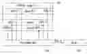
FIG. 1 is a diagram illustrating the operation of a nonvolatile memory device according to a first embodiment of the present disclosure.
Referring to FIG. 1, the nonvolatile memory device includes a memory block unit 100 configured to include a plurality of memory blocks Block 0 to Block N, a page buffer unit 110 coupled to the memory block unit 100, and a redundant memory block Block e 120 coupled to the page buffer unit 110.
FIG. 2 is a flowchart illustrating the operation of the nonvolatile memory device according to the first embodiment of the present disclosure.
A refresh operation of the nonvolatile memory device according to an embodiment of the present disclosure is described below with reference to FIGS. 1 and 2.
First, data (e.g., data DATA_0) of a first memory block (e.g., Block 0) of the memory block unit 100 are read and stored in the page buffer unit 110 at step 210. That is, the data DATA_0 stored in the selected memory block Block 0 are read.
Next, the data DATA_0 stored in the page buffer unit 110 are programmed into the redundant memory block Block e 120 at step 220. That is, the data DATA_0 are temporarily stored in the memory block Block e 120.
The steps 210 and 220 are described in more detail below. The data DATA_0 stored in the first memory block Block 0 are read and temporarily stored using a page buffer of the page buffer unit 110. Next, the data DATA_0 are programmed into the redundant memory block Block e 120 coupled to the page buffer. Here, since the memory block includes a plurality of pages, the data DATA_0 are moved from the memory block Block 0 to the redundant memory block Block e 120 by sequentially performing the read and program operations on a page basis.
Next, the first memory block Block 0 is erased by performing an erase operation.
It is then determined whether the read memory block is the last memory block (i.e., Block N) of the memory block unit 100 at step 230. If, as a result of the determination, the read memory block is determined not to be the last memory block Block N of the memory block unit 100, a block address of the corresponding memory block is increased by 1 at step 240. That is, a next memory block (i.e., Block 1) is selected.
Next, the process returns to step 210. In other words, data DATA_1 stored in the next memory block Block 1 are read and stored in the page buffer unit 110.
Next, the data DATA_1 stored in the page buffer unit 110 are programmed into the first memory block Block 0.
After the above read and program operations are repeatedly performed for each memory block, the data of the first memory block Block 0 are programmed into the redundant memory block Block e 120, the data of the second memory block Block 1 are programmed into the first memory block Block 0, and the data of the last memory block Block N are programmed into the memory block Block N−1.
Furthermore, in general, information about important data elements of the memory device may be stored in the first memory block Block 0. When the memory device is operated, the information about the important data elements is first selected and used. Accordingly, the data DATA_1 stored in the first memory block Block 0 may be moved to the last memory block Block N using the page buffer unit 110. Next, after the first memory block Block 0 is erased, the data DATA_0 programmed into the redundant memory block Block e 120 may be moved to the first memory block Block 0 using the page buffer unit 110.
As described above, the nonvolatile memory device can be refreshed by reprogramming data, stored in a plurality of the memory blocks Block 0 to Block N of the memory block unit 100, into the redundant memory block Block e 120 and a plurality of the memory blocks Block 0 to Block N−1. Accordingly, the retention characteristic of the nonvolatile memory device can be improved.
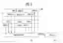
FIG. 3 is a diagram illustrating the operation of a nonvolatile memory device according to a second embodiment of the present disclosure.
Referring to FIG. 3, the nonvolatile memory device includes a memory block unit 100 configured to include a plurality of memory blocks Block 0 to Block N, a page buffer unit 110 coupled to the memory block unit 100, and a redundant memory block Block e (120) coupled to the page buffer unit 110.
The operation of the nonvolatile memory device according to the second embodiment of the present disclosure is described below with reference to FIG. 3.
First, data (e.g., data DATA_0) stored in a first memory block (e.g., Block 0) of the memory block unit 100 are read and stored in the page buffer unit 110. That is, the data DATA_0 of the selected memory block Block 0 are read.
Next, the data DATA_0 stored in the page buffer unit 110 are programmed into the redundant memory block Block e 120. That is, the data DATA_0 are temporarily stored in the memory block Block e 120.
Specifically, the data DATA_0 stored in the first memory block Block 0 are read and temporarily stored using a page buffer of the page buffer unit 110. The stored data DATA_0 are programmed into the redundant memory block Block e 120 coupled to the page buffer. Here, since the memory block includes a plurality of pages, the data DATA_0 are moved from the memory block Block 0 to the redundant memory block Block e 120 by sequentially performing the read and program operations on a page basis.
The first memory block Block 0 is then erased by performing an erase operation.
Next, the data DATA_0 temporarily stored in the redundant memory block Block e 120 are read and temporarily stored in the page buffer unit 110. The data DATA_0 stored in the page buffer unit 110 are then programmed into the first memory block Block 0.
Next, the redundant memory block Block e 120 is erased.
It is then determined whether the corresponding memory block (i.e., the selected memory block Block 0) is the last memory block (i.e., Block N) of the memory block unit 100. If, as a result of the determination, the selected memory block Block 0 is determined not to be the last memory block Block N of the memory block unit 100, a block address of the selected memory block Block 0 is increased by 1, and a next memory block (i.e., Block 1) is selected.
Next, as in the operation for the first memory block Block 0, data DATA_1 stored in the second memory block Block 1 are read and temporarily stored in the page buffer unit 110. The stored data DATA_1 are programmed into the erased first memory block Block 0. After the second memory block Block 1 is erased, the data DATA_0 stored in the redundant memory block Block e 120 are read and temporarily stored in the page buffer unit 110. The stored data DATA_0 are programmed into the erased second memory block Block 1.
If the above read and program operations are repeatedly performed by increasing the block address of a memory block, data stored in a plurality of the memory blocks Block 0 to Block N are temporarily stored in the redundant memory block Block e 120 and then programmed into the original memory blocks Block 0 to Block N again. As a result, a refresh operation is performed on the memory blocks Block 0 to Block N.
According to the present disclosure, data of a memory block are reprogrammed in such a manner that data of a first memory block of a plurality of memory blocks are programmed into a redundant memory block, and data of a second memory block of the memory blocks are read and programmed into the first memory block. Accordingly, a refresh operation capable of improving the retention characteristic of a nonvolatile memory device is provided.
Claims
What is claimed is:1. A method of programming a nonvolatile memory device, the method comprising:
reading first data of a first memory block, storing the first data in a page buffer unit, and then programming the first data into a redundant memory block coupled to the page buffer unit;
reading second data of a second memory block, storing the second data in the page buffer unit, and then programming the second data into the first memory block;
reading third data of a third memory block, storing the third data in the page buffer unit, and then programming the third data into the second memory block;
reading the second data of the first memory block, storing the read second data in the page buffer unit, and then programming the stored second data into the third memory block; and
reading the first data stored in the redundant memory block, storing the read first data in the page buffer unit, and then programming the stored first data into the first memory block.
2. The method of claim 1, further comprising erasing the first memory block after programming the first data into the redundant memory block.
3. The method of claim 1, further comprising erasing the second memory block after programming the second data into the first memory block.
4. The method of claim 1, further comprising erasing the third memory block after programming the third data into the second memory block.
5. The method of claim 1, further comprising erasing the second memory block after programming the second data into the third memory block.
6. A method of operating a nonvolatile memory device comprising first to Nth memory blocks, the method comprising:
reading data of the first memory block and programming the read data into a redundant memory block;
reading data from the second memory block unit to the Nth memory block while increasing an address of each of the second memory block unit to the Nth memory block, and programming the read data into the first to (N−1)th memory block, respectively, wherein N is a natural number;
reading the data programmed into the first memory block and programming the read data into the Nth memory block; and
reading the data programmed into the redundant memory block and programming the read data into the first memory block.
7. The method of claim 6, further erasing a memory block from which data have been read.
8. A method of operating a nonvolatile memory device, which comprises a plurality of memory blocks and a redundant memory block for temporarily storing data during a refresh operation, the method comprising:
reading program data of a selected memory block of the plurality of memory blocks, storing the read program data in a page buffer unit, and programming the stored program data into the redundant memory block coupled to the page buffer unit;
erasing the selected memory block; and
reading the program data stored in the redundant memory block, storing the read program data in the page buffer unit, and programming the stored program data into the selected memory block.
9. The method of claim 8, further comprising, after programming the stored program data into the selected memory block:
determining whether the selected memory block is a last memory block of the plurality of memory blocks;
if, as a result of the determination, the selected memory block is determined not to be the last memory block of the memory blocks, increasing an address of the selected memory block and setting a memory block corresponding to the increased address, from among the plurality of memory blocks, as a newly selected memory block;
reading data programmed into the newly selected memory block and programming the read data into the redundant memory block;
erasing the newly selected memory block; and
reading the data programmed into the redundant memory block, storing the read data into the page buffer unit, and programming the stored data into the newly selected memory block.
Images & Drawings included:
Sources:
- United States Patent and Trademark Office - verify current appl. status at the USPTO↗
Similar patent applications:
- » 20250165341
NONVOLATILE MEMORY DEVICE, OPERATING METHOD OF NONVOLATILE MEMORY DEVICE, AND OPERATING METHOD OF STORAGE DEVICE - » 20200035278
Nonvolatile memory device, operation method of the nonvolatile memory device, and operation method of memory controller controlling the nonvolatile memory device - » 20230410900
NONVOLATILE MEMORY DEVICE, OPERATION METHOD OF A NONVOLATILE MEMORY DEVICE, AND OPERATION METHOD OF A CONTROLLER - » 20200357460
Nonvolatile memory device, operating method of nonvolatile memory device, and storage device including nonvolatile memory device - » 20200286545
Nonvolatile memory device, operating method of nonvolatile memory device, and storage device including nonvolatile memory device - » 20180204620
Nonvolatile memory device, operating method of nonvolatile memory device, and storage device including nonvolatile memory device - » 20220277778
Nonvolatile memory device, operating method of nonvolatile memory device, and electronic device including nonvolatile memory device - » 20110219288
METHOD OF OPERATING NONVOLATILE MEMORY DEVICE, METHOD OF OPERATING CONTROLLER, AND METHOD OF OPERATING MEMORY SYSTEM INCLUDING THE SAME - » 20100208521
Nonvolatile memory device, method of operating nonvolatile memory device and memory system including nonvolatile memory device - » 20200194072
Methods of operating nonvolatile memory devices, methods of operating storage device and storage devices
Recent applications in this class:
- » 20250173261 2025-05-29
MEMORY DEVICE AND MEMORY SYSTEM FOR PERFORMING SWAP OPERATION - » 20250173260 2025-05-29
MEMORY CONTROLLER, STORAGE DEVICE INCLUDING MEMORY CONTROLLER, AND OPERATING METHOD OF MEMORY CONTROLLER - » 20250165393 2025-05-22
METHOD AND SYSTEM FOR IN-LINE ECC PROTECTION - » 20250165392 2025-05-22
MEMORY CONTROLLER FOR SCHEDULING COMMANDS BASED ON RESPONSE FOR RECEIVING WRITE COMMAND, STORAGE DEVICE INCLUDING THE MEMORY CONTROLLER, AND OPERATING METHOD OF THE MEMORY CONTROLLER AND THE STORAGE DEVICE - » 20250165391 2025-05-22
STORAGE DEVICE AND OPERATING METHOD OF THE STORAGE DEVICE - » 20250165390 2025-05-22
OPERATING A STORAGE SYSTEM - » 20250165389 2025-05-22
APPARATUS AND METHOD FOR DISTRIBUTING AND STORING WRITE DATA IN PLURAL MEMORY REGIONS - » 20250165388 2025-05-22
HOST SYSTEMS, MEMORY SYSTEMS, STORAGE MEDIUMS, AND ELECTRONIC APPARATUSES AND OPERATION METHODS THEREOF - » 20250156317 2025-05-15
MANAGEMENT OF STORAGE RESOURCES ALLOCATED FROM NON-VOLATILE MEMORY DEVICES TO USERS - » 20250156316 2025-05-15
VIRTUAL INDEXING IN A MEMORY DEVICE