Method and apparatus for dealing with write errors when writing information data into flash memory devices
US20100332891A1
2010-12-30
12/819,432
2010-06-21
✅ Patent granted
US 8,352,780 B2
2013-01-08
-
-
Joshua P Lottich
2031-02-18
Abstract:
For writing, flash memory devices are physically accessed in a page-oriented mode, but such devices are not error-free in operation. According to the invention, when writing information data in a bus write cycle in a sequential manner into flash memory devices assigned to a common data bus, at least one of said flash memory devices is not fed for storage with a current section of said information data. In case an error is occurring while writing a current information data section into a page of a current one of said flash memory devices, said current information data section is written into a non-flash memory. During the following bus write cycle, while the flash memory device containing that defective page is normally idle, that idle time period is used for copying the corresponding stored section of said information data from said non-flash memory to a non-defect page of that flash memory device.
Inventors:
- Thomas Brune 27 🇩🇪 Hannover, Germany
- Michael Drexler 11 🇩🇪 Gehrden, Germany
- Dieter Haupt 2 🇩🇪 Lueneburg, Germany
Assignee:
- THOMSON LICENSING 1,193 🇫🇷 Issy Les Moulineaux, France
Interested in similar patents?
Get notified when new applications in this technology area are published.
Classification:
G06F11/00 IPC
Error detection; Error correction; Monitoring
G06F11/141 » CPC main
Error detection; Error correction; Monitoring; Responding to the occurrence of a fault, e.g. fault tolerance; Error detection or correction of the data by redundancy in operation; Saving, restoring, recovering or retrying at machine instruction level for bus or memory accesses
G06F12/0246 » CPC further
Accessing, addressing or allocating within memory systems or architectures; Addressing or allocation; Relocation; User address space allocation, e.g. contiguous or non contiguous base addressing; Free address space management; Memory management in non-volatile memory, e.g. resistive RAM or ferroelectric memory in block erasable memory, e.g. flash memory
G06F2212/7209 » CPC further
Indexing scheme relating to accessing, addressing or allocation within memory systems or architectures; Details relating to flash memory management Validity control, e.g. using flags, time stamps or sequence numbers
G11C29/70 » CPC further
Checking stores for correct operation ; Subsequent repair ; Testing stores during standby or offline operation Masking faults in memories by using spares or by reconfiguring
G06F11/20 IPC
Error detection; Error correction; Monitoring; Responding to the occurrence of a fault, e.g. fault tolerance; Error detection or correction of the data by redundancy in hardware using active fault-masking, e.g. by switching out faulty elements or by switching in spare elements
Description
FIELD OF THE INVENTION
The invention relates to a method and to an apparatus for dealing with write errors when writing information data into flash memory devices, wherein multiple flash memory devices are assigned to a common data bus and in a bus write cycle these flash memory devices are sequentially fed with said information data for storage therein.
BACKGROUND OF THE INVENTION
NAND flash semiconductor devices, as used in storage devices like e.g. the Grass Valley VENOM solid state recorders, are not error-free in operation. For writing, flash memory devices are physically accessed in a page-oriented mode, whereby one ‘page’ includes e.g. 1024 or 2048 data words and related error correction code. Future flash devices will have a 4096 bytes page size. Erase operations on a specific flash memory can be carried out on specific-size data ‘blocks’ only. Such data block may include 64 pages. Some of the memory defects are already detected during production of the storage devices and the corresponding memory locations or pages are marked as ‘bad’ and not usable. Specific circuitry avoids information data being stored at such ‘bad’ locations. However, further memory defects will occur during the lifetime and operation of a flash semiconductor. A related processing must prevent that information data intended to be written in such newly defect sections of a flash memory will not be lost. A corresponding processing is described e.g. in WO2007/080031 A1 and in WO2006/108755 A1.
SUMMARY OF THE INVENTION
A disadvantage of such processing is that the information data, which was intended to be written to defective areas of a flash memory and which is cached e.g. into an SRAM memory, is to be copied to ‘save’ areas within the flash memory after the actual recording or take has been finished. This takes some extra time, and the corresponding information is not secured while the information data are not yet stored into the flash memory section of the recording apparatus. Intermediate malfunctions of the recording apparatus, e.g. an operating error or a power-down caused by an empty battery, will lead to information loss. However, such storage malfunctions are not acceptable in a professional storage system.
A problem to be solved by the invention is to deal properly with information data write errors in flash memory devices, such that the error handling occurs during a write cycle for multiple flash memories attached to a common bus. This problem is solved by the method disclosed in claim 1. An apparatus that utilises this method is disclosed in claim 2.
According to the invention, the dynamic defect management is not processed after a recording has been finished but in parallel to that recording.
- Advantageously, the required size of the SRAM memory, which stores information data that were initially intended for storage in defect flash memory pages, can be smaller. Because the I/O data rate of recently commercially available NAND flash devices has been increased with respect to that of previous flash device types, the available bandwidth now remaining can be used for the inventive internal copy process.
- A save storage of all information data is facilitated, even in case of currently unknown types of defects in flash memory devices. No information will be lost in case of recording apparatus malfunction or a system halt due to low battery status occurring between the beginning of a recording and the end of a take.
In principle, the inventive method is suited for dealing with write errors when writing information data into flash memory devices, wherein two or more flash memory devices are assigned to a common data bus and in a bus write cycle two or more of these flash memory devices are sequentially fed with said information data for storage therein, said method including the steps:
- in said bus write cycle, at least one of said flash memory devices is not fed for storage with a current section of said information data;
- at least in case an error is occurring while writing a current section of said information data into a page of a current one of said flash memory devices, writing said current section of said information data into a non-flash memory;
- during the following bus write cycle, while the flash memory device containing that defective page is normally idle, that idle time period is used for copying the corresponding stored section of said information data from said non-flash memory to an assumed save or non-defect page of that flash memory device.
In principle the inventive apparatus is suited for dealing with write errors when writing information data into flash memory devices, said apparatus including:
- at least one common data bus;
- two or more flash memory devices and at least one non-flash memory assigned to each one of said data buses, wherein each one of said data buses receives application data via a FIFO device and wherein in a bus write cycle two or more of these flash memory devices per bus are sequentially fed with said information data for storage therein,
- and wherein in said bus write cycle at least one of said flash memory devices is not fed for storage with a current section of said information data,
- and wherein at least in case an error is occurring while writing a current section of said information data into a page of a current one of said flash memory devices, said current section of said information data is written into said non-flash memory;
- and wherein during the following bus write cycle, while the flash memory device containing that defective page is normally idle, that idle time period is used for copying the corresponding stored section of said information data from said non-flash memory to an assumed save or non-defect page of that flash memory device.
Advantageous additional embodiments of the invention are disclosed in the respective dependent claims.
BRIEF DESCRIPTION OF THE DRAWINGS
Exemplary embodiments of the invention are described with reference to the accompanying drawings, which show in:
FIG. 1 known memory write cycle on a bus;
FIG. 2 inventive memory write cycle on a bus, in a first write sequence;
FIG. 3 successive completed bus write cycles with different flash memory being idle;
FIG. 4 inventive copy processing.
DETAILED DESCRIPTION
The write access to known NAND flash memory devices is performed in two steps:
- An amount of e.g. 2048 or 4096 bytes (i.e. one ‘page’) of information data is collected from the I/O pin of a flash memory device and is stored into an internal buffer memory. The content of the internal buffer memory (one page) is copied to the flash memory area.
On one hand, the above copy process is relatively slow, typically 700 μs copy time for one page. On the other hand, the access to the internal buffer memory from the outside of the flash memory device is relatively fast: a bus data rate of 20-40 MB/s for current devices and up to 200 MB/s for next-generation flash memory devices.
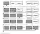
For achieving an increased data rate, the NAND flash devices can be arranged in the recording apparatus as a matrix of memories (as depicted in FIG. 1 of WO2007/080031 A1 and in FIG. 1 of WO2006/108755 A1) that is controlled by several buses, to each bus B of which N NAND flash devices Device0, Device1, Device2, . . . , DeviceN-2, DeviceN-1 are connected, as shown in FIG. 1 of the current application for a single one of the buses. The first row represents a first write period for Device0, the second row represents a second write period for Device1, and so on. The last row represents the last write period for DeviceN-1. The number of NAND flash devices connected to a bus is calculated with respect to the above-mentioned bus data rate and to the above-mentioned copy time, in order to meet the requirements of the application data rate. The writing is performed as an interleaved multiplex. State-of-the-art architectures (e.g. the VENOM FlashPak mentioned above) do not provide bandwidth for additional data transfers in case of write errors.
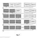
According to the invention, extra bandwidth (with respect to the required application bandwidth) is added by either adding one or more additional flash memory devices to bus or buses B, as shown in FIG. 2, or by using faster flash memory devices. For example, in case N flash memory devices are needed on a bus for fulfilling the original bandwidth requirements, N+1 flash memory devices present on the bus will provide an I/O bandwidth that is increased by a factor of (N+1)/N. This additional bandwidth is used for facilitating the internal copy process from the SRAM memory to the flash devices within the ongoing interleaved multiplex. This extra bandwidth will only be used when flash page write errors will occur. Both, the additional bandwidth for the internal copy process of the flash devices and the interface band-width are selected so as to enable the inventive page write error defect management.
During an error-free page writing operation period, one flash device—e.g. Device0 in FIG. 2—on bus B is not used for writing within a current write cycle. FIG. 2 shows one write cycle starting with Device1 and ending with DeviceN. The first row represents a first write period for Device1, the second row represents a second write period for Device1, and so on. The last row represents the last write period for DeviceN. During the following write cycle, another one of the flash devices on bus B will not be used in that write cycle but Device0 is used instead in that write cycle. A controller or a corresponding program for a processor, which controller or processor is not depicted:
- controls the write operation into the flash memories Device0 to DeviceN attached to bus B;
- controls which one of the flash memories on bus B is not used in a current bus write cycle;
- checks whether a flash memory on bus B—or any other corresponding status data—has signalled a writing error or a newly defective writing area;
- controls the corresponding information data transfer to and from a non-flash memory attached to bus B as described in connection with FIG. 4.
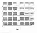
FIG. 3 depicts a successive sequence of (completed) example bus write cycles, in each of which bus write cycles a different flash device is idle on bus B, starting with Device0 in bus write cycle 0 and ending with DeviceN in. After N+1 write cycles each flash device had been idle bus write cycle N.
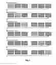
In FIG. 4a, in case a writing error in flash memory e.g. Device0 or a newly defective writing area in that flash memory is signalled (by that flash memory), the information data intended for writing into a defective flash page will instead be temporally stored in a non-flash memory, e.g. an SRAM memory.
- As an alternative, the page information data written into a current flash memory is in parallel also written into the SRAM memory while the previously stored information data in the SRAM memory is deleted or overwritten at the appropriate time, which means that the storage capacity of the SRAM memory needs to be larger than in the other embodiment.
- During the following bus write cycle, while the flash memory device containing that defective page is normally idle, that idle time period is used for initialising and carrying out a copy operation from the SRAM memory to an assumed save or non-defective flash page of that flash memory device, as shown in FIG. 4b. Thereafter the processing continues in the normal way, as depicted in FIG. 4c. The FIFO arranged at the input of bus B is used for compensating the factor (N+1)/N-increased data rate on flash bus B.
In most cases, three or more flash memory devices Device0, Device1, . . . , DeviceN-1 are assigned or connected to the common data bus B, and in a bus write cycle two or more of these flash memory devices are sequentially fed with the information data for storage therein. Within a cache memory device, in a first step the information data are written into the internal cache memory section of the flash device and in a second step are transferred or programmed from that cache memory to the flash memory kernel.
- However, in case a ‘cache mode’ is used for the flash memories, the flash memory device allows to write the information data into the cache memory section of the flash device while the previously received information data are programmed (i.e. stored) from the cache memory into the flash memory kernel (the flash memory device has two cache memory sections or two cache memories). In such ‘cache mode’ operation, at least two flash memory devices Device0, Device1, . . . , DeviceN-1 are assigned or connected to the common data bus B.
Claims
1. A method for dealing with write errors when writing information data into flash memory devices, wherein two or more flash memory devices are assigned to a common data bus and in a bus write cycle two or more of these flash memory devices are sequentially fed with said information data for storage therein, said method comprising the steps:
in said bus write cycle, at least one of said flash memory devices is not fed for storage with a current section of said information data;
at least in case an error is occurring while writing a current section of said information data into a page of a current one of said flash memory devices, writing said current section of said information data into a non-flash memory;
during the following bus write cycle, while the flash memory device containing that defective page is normally idle, that idle time period is used for copying the corresponding stored section of said information data from said non-flash memory to an assumed save or non-defect page of that flash memory device.
2. A method according to claim 1, wherein in each one of successive bus write cycles a different one of said flash memory devices on said bus is not fed for storage with a current section of said information data.
3. A method according to claim 1, wherein said non-flash memory is an SRAM memory.
4. A method according to claim 1, wherein said flash memory devices are operating in a cache mode.
5. A method according to claim 1, wherein said flash memory devices are not operating in a cache mode and wherein three or more flash memory devices are assigned to said common data bus.
6. An apparatus for dealing with write errors when writing information data into flash memory devices, said apparatus comprising:
at least one common data bus;
two or more flash memory devices and at least one non-flash memory assigned to each one of said data buses,
wherein each one of said data buses receives application data via a FIFO device and wherein in a bus write cycle two or more of these flash memory devices per bus are sequentially fed with said information data for storage therein,
and wherein in said bus write cycle at least one of said flash memory devices is not fed for storage with a current section of said information data,
and wherein at least in case an error is occurring while writing a current section of said information data into a page of a current one of said flash memory devices, said current section of said information data is written into said non-flash memory;
and wherein during the following bus write cycle, while the flash memory device containing that defective page is normally idle, that idle time period is used for copying the corresponding stored section of said information data from said non-flash memory to an assumed save or non-defect page of that flash memory device.
7. An apparatus according to claim 6, wherein in each one of successive bus write cycles a different one of said flash memory devices on said bus is not fed for storage with a current section of said information data.
8. An apparatus according to claim 6, wherein said non-flash memory is an SRAM memory.
9. An apparatus according to claim 6, wherein said flash memory devices are operating in a cache mode.
10. An apparatus according to claim 6, wherein said flash memory devices are not operating in a cache mode and wherein three or more flash memory devices are assigned to said common data bus.
Images & Drawings included:
Sources:
- United States Patent and Trademark Office - verify current appl. status at the USPTO↗
Recent applications in this class:
- » 20250225031 2025-07-10
METHOD, DEVICE, AND COMPUTER PROGRAM PRODUCT FOR ADJUSTING DATA PLACEMENT - » 20240320097 2024-09-26
MEMORY SYSTEM - » 20240143443 2024-05-02
METHOD AND APPARATUS FOR REPAIRING HANGING IN COMMUNICATION BUS, ELECTRONIC DEVICE, AND STORAGE MEDIUM - » 20240045765 2024-02-08
STORAGE DEVICE AND STORAGE SYSTEM - » 20230116945 2023-04-20
A MULTI-PART COMPARE AND EXCHANGE OPERATION - » 20230068583 2023-03-02
System and method for fault identification and fault handling in a multiport power sourcing device - » 20220398158 2022-12-15
Memory safety interface configuration - » 20220269563 2022-08-25
Safe-stating a system interconnect within a data processing system - » 20220206899 2022-06-30
Method and apparatus to support instruction replay for executing idempotent code in dependent processing in memory devices - » 20210279138 2021-09-09
Data storage device and method of operating the same
Recent applications for this Assignee:
- » 20190162978 2019-05-30
Apparatus and a method for generating data representative of a pixel beam - » 20190110109 2019-04-11
ELECTRONIC PROGRAM LISTING DISPLAYING HIGH DYNAMIC RANGE AND NON-HIGH DYNAMIC RANGE PROGRAM SELECTIONS - » 20190028750 2019-01-24
MEDIA ASSET RECOMMENDATIONS AND SORTING BASED ON RENDERING DEVICE PROPERTIES - » 20190020923 2019-01-17
Method and apparatus for inhibiting the interruption of content being consumed by a user - » 20190014083 2019-01-10
URL FILTERING METHOD AND DEVICE - » 20190007740 2019-01-03
CONTENT RECOMMENDATIONS ASSOCIATED WITH CONTEXT PROVIDED BY A VIEWER - » 20180376213 2018-12-27
ASSOCIATION BETWEEN A CLIENT AND A MULTIMEDIA DEVICE - » 20180376205 2018-12-27
METHOD AND APPARATUS FOR REMOTE PARENTAL CONTROL OF CONTENT VIEWING IN AUGMENTED REALITY SETTINGS - » 20180375706 2018-12-27
Method and apparatus for receiving a reduced peak to average power ratio signal - » 20180374271 2018-12-27
Key lights direction detection