Easily stackable dies
US20110023574A1
2011-02-03
12/796,101
2010-06-08
✅ Patent granted
US 8,424,357 B2
2013-04-23
-
-
Bena Miller
Muncy, Geissler, Olds & Lowe, PLLC
2030-09-10
Abstract:
A die includes upper contacts, lower contacts and conductive elements. The upper contacts are formed on an upper face of the die. The upper contacts include a non-connected upper contact and connected upper contacts. The lower contacts are formed on a lower face of the die. The lower contacts include a non-connected lower contact and connected lower contacts. Each of the conductive elements connects a related one of the connected upper contacts to a related one of the connected lower contacts.
Inventors:
- Kuei-Wu Chu 9 🇹🇼 Taoyuan County, Taiwan
- Jimmy Liang 6 🇹🇼 Taoyuan County, Taiwan
- Leo Lu 5 🇹🇼 Taoyuan County, Taiwan
Assignee:
- MAO BANG ELECTRONIC CO., LTD. 16 🇹🇼 Taoyuan County, Taiwan
- Aflash Technology, Co., Ltd. 4 🇹🇼 Luzhu Township, Taoyuan County, Taiwan
Applicant:
Interested in similar patents?
Get notified when new applications in this technology area are published.
Classification:
H01L25/0657 » CPC main
Assemblies consisting of a plurality of individual semiconductor or other solid state devices ; Multistep manufacturing processes thereof all the devices being of a type provided for in the same subgroup of groups - , e.g. assemblies of rectifier diodes the devices not having separate containers the devices being of a type provided for in group Stacked arrangements of devices
H01L22/34 » CPC further
Testing or measuring during manufacture or treatment; Reliability measurements, i.e. testing of parts without further processing to modify the parts as such; Structural arrangements therefor; Structural arrangements specially adapted for testing or measuring during manufacture or treatment, or specially adapted for reliability measurements Circuits for electrically characterising or monitoring manufacturing processes, e. g. whole test die, wafers filled with test structures, on-board-devices incorporated on each die, process control monitors or pad structures thereof, devices in scribe line
H01L2225/06513 » CPC further
Details relating to assemblies covered by the group but not provided for in its subgroups; All the devices being of a type provided for in the same subgroup of groups - the devices not having separate containers the devices being of a type provided for in group; Stacked arrangements of devices Bump or bump-like direct electrical connections between devices, e.g. flip-chip connection, solder bumps
H01L2225/06527 » CPC further
Details relating to assemblies covered by the group but not provided for in its subgroups; All the devices being of a type provided for in the same subgroup of groups - the devices not having separate containers the devices being of a type provided for in group; Stacked arrangements of devices Special adaptation of electrical connections, e.g. rewiring, engineering changes, pressure contacts, layout
H01L2225/06551 » CPC further
Details relating to assemblies covered by the group but not provided for in its subgroups; All the devices being of a type provided for in the same subgroup of groups - the devices not having separate containers the devices being of a type provided for in group; Stacked arrangements of devices Conductive connections on the side of the device
H01L2924/0002 » CPC further
Indexing scheme for arrangements or methods for connecting or disconnecting semiconductor or solid-state bodies as covered by; Technical content checked by a classifier Not covered by any one of groups , and
H01L2924/00 » CPC further
Indexing scheme for arrangements or methods for connecting or disconnecting semiconductor or solid-state bodies as covered by
B21C3/16 IPC
Profiling tools for metal drawing; Combinations of dies and mandrels Mandrels; Mounting or adjusting same
B21D37/16 IPC
Tools as parts of machines covered by this subclass Heating or cooling
Description
BACKGROUND OF INVENTION
1. Field of Invention
The present invention relates to a die and, more particularly, to a die that can easily be stacked with other dies and that is made by masks that can easily be designed and managed.
2. Related Prior Art
Traditionally, different masks are used to make different layouts on upper and lower faces of a die according to different contacts and layouts. A die can be stacked with other dies. After the dies are stacked, wires are used to connect the contacts of each of the dies to the contacts of another one of the dies. However, the design of a system of such dies is limited, and the stacking of such dies is not easy. Moreover, the contacts and layout on the upper face of the die and the contacts and layout on the lower face of the die are made by different masks. The masks cannot be used in place of each other. The management of the masks is troublesome.
The present invention is therefore intended to obviate or at least alleviate the problems encountered in prior art.
SUMMARY OF INVENTION
It is the primary objective of the present invention to provide a die that can easily be stacked with other dies.
To achieve the foregoing objective, the die includes upper contacts, lower contacts and conductive elements. The upper contacts are formed on an upper face of the die. The upper contacts include a non-connected upper contact and connected upper contacts. The lower contacts are formed on a lower face of the die. The lower contacts include a non-connected lower contact and connected lower contacts. Each of the conductive elements connects a related one of the connected upper contacts to a related one of the connected lower contacts.
Other objectives, advantages and features of the present invention will be apparent from the following description referring to the attached drawings.
BRIEF DESCRIPTION OF DRAWINGS
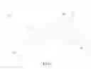
The present invention will be described via detailed illustration of the preferred embodiment referring to the drawings wherein:
FIG. 1 is a perspective view of a die according to the preferred embodiment of the present invention;
FIG. 2 is another perspective view of the die shown in FIG. 1;
FIG. 3 is a perspective view of a stack of dies as shown in FIG. 1; and
FIG. 4 is a perspective view of a control circuit board connected to the stack of dies shown in FIG. 3.
DETAILED DESCRIPTION OF PREFERRED EMBODIMENT
Referring to FIGS. 1 and 2, there is shown a die 1 according to the preferred embodiment of the present invention. The die 1 includes an upper face 11, a lower face 12 and a lateral face 13 extending between the upper face 11 and the lower face 12.
There are upper contacts 2 formed on the upper face 11 of the die 1. The upper contacts 2 include a non-connected upper contact 21 and connected upper contacts 22. The first upper contact 2 is preferably the non-connected upper contact 21. The other upper contacts 2 are the connected upper contacts 22.
There are lower contacts 2a formed on the lower face 12 of the die 1. The lower contacts 2a include a non-connected lower contact 21a and connected lower contacts 22a. The last lower contact 2a is preferably the non-connected lower contact 21a. The other lower contacts 2a are the connected lower contacts 22a.
There are conductive elements 3 for connecting the connected upper contacts 22 to the connected lower contacts 22a. Each of the conductive elements 3 includes an upper conductive portion 31 extending on the upper face 11 of the die 1, a lower conductive portion 32 extending on the lower face 12 of the die 1, and a lateral conductive portion 33 extending to the upper conductive portion 31 from the lower conductive portion 32 on the lateral face 13 of the die 1.
Referring to FIG. 3, there is shown a stack of dies 1 as shown in FIGS. 1 and 2. The first connected lower contact 22 of each of the dies 1 is connected to the non-connected upper contact 21 of a lower one of the dies 1. The second connected lower contact 22 of the upper die 1 is connected to the first connected upper contact 22 of the lower die 1. The third connected lower contact 22 of the upper die 1 is connected to the second connected upper contact 22 of the lower die 1. The fourth connected lower contact 22 of the upper die 1 is connected to the third connected upper contact 22 of the lower die 1.
Referring to FIG. 4, a control circuit board 4 is connected to the stack of dies 1. More particularly, the control circuit board 4 is directly connected to the first die 1. For example, the second, third and fourth connected contacts 22 of the first die 1 are used to control the second, third and fourth dies 1, respectively. The non-connected contact 21 of the first die 1 is used to test whether the lateral conductive portion 33 of the conductive elements 3 of any one of the dies 1 is connected. Thus, there is no need for any jumper to use the stack of dies 1.
The present invention has been described via the detailed illustration of the preferred embodiment. Those skilled in the art can derive variations from the preferred embodiment without departing from the scope of the present invention. Therefore, the preferred embodiment shall not limit the scope of the present invention defined in the claims.
Claims
1. A die 1 including:
an upper face 11;
a lower face 12;
a lateral face 13 extending between the upper and lower faces 11, 12;
upper contacts 2 formed on the upper face 11 of the die 1, wherein the upper contacts 2 include a non-connected upper contact 21 and connected upper contacts 22;
lower contacts 2a formed on the lower face 12 of the die 1, wherein the lower contacts 2a include a non-connected lower contact 21a and connected lower contacts 22a; and
conductive elements 3 each for connecting a related one of the connected upper contacts 22 to a related one of the connected lower contacts 22a.
2. The die according to claim 1, wherein a first one of the upper contacts 2 is the non-connected upper contact 21.
3. The die according to claim 1, wherein a last one of the lower contacts 2a is the non-connected lower contact 21a.
4. The die according to claim 1, wherein each of the conductive elements 3 includes an upper conductive portion 31 extending on the upper face 11 of the die 1, a lower conductive portion 32 extending on the lower face 12 of the die 1, and a lateral conductive portion 33 extending on the lateral face 13 of the die 1.
Images & Drawings included:


Sources:
- United States Patent and Trademark Office - verify current appl. status at the USPTO↗
Recent applications in this class:
- » 20250293212 2025-09-18
SEMICONDUCTOR PACKAGES - » 20250293211 2025-09-18
HEAT DISSIPATION FOR STACKED INTEGRATED CIRCUIT DEVICES - » 20250293210 2025-09-18
SYSTEMS AND METHODS FOR PACKAGING A SEMICONDUCTOR DEVICE - » 20250286021 2025-09-11
SEMICONDUCTOR PACKAGE - » 20250286020 2025-09-11
SEMICONDUCTOR BONDING STRUCTURE - » 20250286019 2025-09-11
SEMICONDUCTOR PACKAGE - » 20250286018 2025-09-11
METHOD OF FABRICATING SEMICONDUCTOR BONDING STRUCTURE - » 20250286017 2025-09-11
SEMICONDUCTOR DEVICE - » 20250279399 2025-09-04
SEMICONDUCTOR DEVICES AND MANUFACTURING METHODS OF THE SAME - » 20250279398 2025-09-04
VERTICAL INTERCONNECT STRUCTURES IN THREE-DIMENSIONAL INTEGRATED CIRCUITS
Recent applications for this Assignee:
- » 20150270448 2015-09-24
Flip-chip LED, method for manufacturing the same and flip-chip package of the same - » 20120181065 2012-07-19
Multi-Layered Circuit Board Device - » 20120091595 2012-04-19
Layered Integrated Circuit Apparatus - » 20120074558 2012-03-29
Circuit Board Packaged with Die through Surface Mount Technology - » 20110291291 2011-12-01
Silicon Chip Having Penetrative Connection Holes - » 20110260300 2011-10-27
Wafer-bump structure - » 20110260300 2011-10-27
Wafer-bump structure - » 20110228487 2011-09-22
Integrated circuit card - » 20110228487 2011-09-22
Integrated circuit card - » 20110176021 2011-07-21
Image-Processing Integrated Circuit