Flip chip package structure with heat dissipation enhancement and its application
US20110221047A1
2011-09-15
13/043,782
2011-03-09
✅ Patent granted
US 8,659,128 B2
2014-02-25
-
-
Howard Weiss | Steven Rao
Muncy, Geissler, Olds & Lowe, P.C.
2031-03-15
Abstract:
A flip chip package structure includes a chip placed under a lead frame, a bump on the upper surface of the chip that is electrically connected to the lead of the lead frame, and a backside metal on the lower surface of the chip that is exposed outside an encapsulant encapsulating the chip and a portion of the lead frame.
Inventors:
- Yu-Lin Yang 3 🇹🇼 Xiyu Township, Taiwan
- Lih-Ming Doong 2 🇹🇼 Zhunan Township, Taiwan
- Yu-Lin Yang 1 🇹🇼 Xiyu Township, Penghu County, Taiwan
- Lih-Ming Doong 1 🇹🇼 Zhunan Township, Miaoli County, Taiwan
Assignee:
- RICHTEK TECHNOLOGY CORP. 225 🇹🇼 Hsinchu, Taiwan
Applicant:
Interested in similar patents?
Get notified when new applications in this technology area are published.
Classification:
H01L23/4334 » CPC main
Details of semiconductor or other solid state devices; Arrangements for cooling, heating, ventilating or temperature compensation ; Temperature sensing arrangements; Fillings or auxiliary members in containers or encapsulations selected or arranged to facilitate heating or cooling; Auxiliary members in containers characterised by their shape, e.g. pistons Auxiliary members in encapsulations
H01L23/49572 » CPC further
Details of semiconductor or other solid state devices; Arrangements for conducting electric current to or from the solid state body in operation, e.g. leads, terminal arrangements ; Selection of materials therefor consisting of soldered constructions; Lead-frames or other flat leads consisting of thin flexible metallic tape with or without a film carrier
H01L2224/73253 » CPC further
Indexing scheme for arrangements for connecting or disconnecting semiconductor or solid-state bodies and methods related thereto as covered by; Means for bonding being of different types provided for in two or more of groups; Location after the connecting process on different surfaces Bump and layer connectors
H01L23/495 IPC
Details of semiconductor or other solid state devices; Arrangements for conducting electric current to or from the solid state body in operation, e.g. leads, terminal arrangements ; Selection of materials therefor consisting of soldered constructions Lead-frames or other flat leads
Description
FIELD OF THE INVENTION
The present invention is related generally to a flip chip package structure and, more particularly, to a flip chip package structure with heat dissipation enhancement and its application.
BACKGROUND OF THE INVENTION
The flip chip package is one of the chip package techniques. As compared with the traditional chip packages where the chip is attached to a pad and then wire bonded to the electrical connection pads on a substrate, the flip chip package is distinguished by growing bumps from the electrical connection pads on the chip and then flipping the chip over to be bonded to the electrical connection pads on a substrate with the bumps. The flip chip package contributes to effective heat dissipation while ensuring low signal interference, good electrical properties and minimum connection circuit loss. In fine pitch applications, high frequency or high input/output (I/O) pin count, benefits of the flip chip package can be fully demonstrated.
The future trend for electronic products is toward compactness, high speed and high pin count while the traditional lead frame based package is not applicable and will be limited to low-end/low-cost products. The development of the flip chip package will remain in pursuing applications of high pin count and fine pitch. Hence, there is a need of a flip chip package structure with heat dissipation enhancement.
SUMMARY OF THE INVENTION
An objective of the present invention is to provide a flip chip package structure with heat dissipation enhancement.
According to the present invention, a flip chip package structure with heat dissipation enhancement includes a lead frame having a lead, a chip having an upper surface formed with a bump thereon that is electrically connected to the lead and a lower surface provided with a backside metal for heat dissipation, and an encapsulant encapsulating the chip and the lead frame but leaving the backside metal exposed outside.
BRIEF DESCRIPTION OF THE DRAWINGS
These and other objectives, features and advantages of the present invention will become apparent to those skilled in the art upon consideration of the following description of the preferred embodiments of the present invention taken in conjunction with the accompanying drawings, in which:
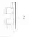
FIG. 1 shows a chip structure used in a flip chip package structure according to the present invention;
FIG. 2 is a first embodiment according to the present invention;
FIG. 3 is a second embodiment according to the present invention; and
FIG. 4 shows an application of the flip chip package structure of FIG. 2.
DETAILED DESCRIPTION OF THE INVENTION
FIG. 1 shows a chip structure used in a flip chip package structure according to the present invention, in which the upper surface of a chip 10 has bumps 12 at electrical connections to be bonded to an external circuit, and the lower surface of the chip 10 has a backside metal 14 attached thereto for transferring heat outward from the chip 10.
FIG. 2 is a first embodiment according to the present invention, which includes a lead frame 16 having leads 162, and an encapsulant 18 encapsulating the bumps 12, a portion of the chip 10, and a portion of the lead frame 16. In this package structure, the chip 10, rather than flipped over as required by the conventional flip chip package structures, is directly placed under the lead frame 16 for electrical connections between the leads 162 and the bumps 12, yet the resultant structure possesses the advantages of low signal interference, good electrical properties, minimum connection circuit loss and effective heat dissipation as those provided by the conventional flip chip package structures. The backside metal 14 is exposed outside the encapsulant 18 for the chip 10 to dissipate heat to the ambient environment directly, thereby improving heat dissipation. In this embodiment, the leads 162 of the lead frame 16 are partially covered by the encapsulant 18 with the remained part as outer leads.
FIG. 3 is a second embodiment according to the present invention. Similar to that of FIG. 2, the chip 10 is placed under the lead frame 16 so as for the electrical connections between the leads 162 and the bumps 12, and the backside metal 14 is exposed outside an encapsulant 20 for heat dissipation enhancement. Different from that of FIG. 2, however, the lead frame 16 in this embodiment is fully encapsulated by the encapsulant 20 so that there are no outer leads extended outside the encapsulant 20 but only partial lower surfaces 164 of the leads 162 are exposed.
FIG. 4 shows an application of the flip chip package structure of FIG. 2 that is placed on a circuit board 22, and has the chip 10 electrically connected to metal 24 of the circuit board 22 through the bumps 12 and the leads 162, and the backside metal 14 in thermal contact with a thermally conductive material 26 on the circuit board 22. The backside metal 14 may be soldered to the thermally conductive material 26; or, alternatively, applied with a thermally conductive adhesive between the backside metal 14 and the thermally conductive material 26. Heat generated by the working chip 10 is transferred to the thermally conductive material 26 through the backside metal 14, so as to maintain the chip 10 working under a stable temperature condition. In other embodiments, the thermally conductive material 26 on the circuit board 22 is a portion of the same metal layer from which is made the metal 24 on the circuit board 22.
While the present invention has been described in conjunction with preferred embodiments thereof, it is evident that many alternatives, modifications and variations will be apparent to those skilled in the art. Accordingly, it is intended to embrace all such alternatives, modifications and variations that fall within the spirit and scope thereof as set forth in the appended claims.
Claims
What is claimed is:1. A flip chip package structure with heat dissipation enhancement, comprising:
a lead frame having a lead;
a chip having a bump on an upper surface thereof and a backside metal on a lower surface thereof, placed under the lead frame with the bump electrically connected to the lead; and
an encapsulant encapsulating the chip and the lead frame but exposing the backside metal to be in contact with a thermally conductive material on an external circuit board.
2. The flip chip package structure of claim 1, wherein the encapsulant encapsulates only a portion of the chip, the bump, only a portion of the lead frame to expose a portion of the lead.
3. The flip chip package structure of claim 2. wherein the exposed portion of the lead is a lower surface of the lead.
4. An application of the flip chip package structure of claim 1, comprising a circuit board having a metal electrically connected to the lead and a thermally conductive material in thermal contact with the backside metal.
Images & Drawings included:


Sources:
- United States Patent and Trademark Office - verify current appl. status at the USPTO↗
Recent applications in this class:
- » 20250246514 2025-07-31
ELECTRONIC PACKAGE AND METHOD OF FORMING THE SAME - » 20250201664 2025-06-19
LIQUID METAL ENCAPSULATION DEVICE - » 20250149405 2025-05-08
SEMICONDUCTOR DEVICE, ELECTRIC POWER CONVERSION UNIT AND METHOD FOR MANUFACTURING SEMICONDUCTOR DEVICE - » 20250149404 2025-05-08
ELECTRONIC COMPONENT-INCORPORATING SUBSTRATE - » 20250079261 2025-03-06
SEMICONDUCTOR PACKAGES WITH THERMAL DISSIPATION - » 20250062188 2025-02-20
SEMICONDUCTOR PACKAGES AND MANUFACTURING METHOD OF THE SAME - » 20240363488 2024-10-31
SEMICONDUCTOR PACKAGES HAVING THERMAL CONDUCTIVE PATTERN - » 20240312868 2024-09-19
SEMICONDUCTOR DEVICE - » 20240282668 2024-08-22
PROTECTION DAM FOR A POWER MODULE WITH SPACERS - » 20240274505 2024-08-15
ELECTRONIC PACKAGE AND MANUFACTURING METHOD THEREOF
Recent applications for this Assignee:
- » 20160043627 2016-02-11
Over-voltage protection circuit and over-voltage protection method - » 20150372602 2015-12-24
Voltage converting controller, voltage converting circuit, and control method for voltage converting - » 20150372599 2015-12-24
Voltage converting controller, voltage converting circuit, and control method for voltage converting - » 20150208189 2015-07-23
Device and method for detecting force factor of loudspeaker - » 20150137611 2015-05-21
Power management unit and wireless power system using the same - » 20150109060 2015-04-23
PROCESS, VOLTAGE AND TEMPERATURE COMPENSATED OSCILLATOR - » 20150009719 2015-01-08
Soft-start switching power converting apparatus with pulse-frequency modulation technique - » 20140320041 2014-10-30
Light emitting diode driver - » 20140286057 2014-09-25
Switching power converting apparatus, switching controller for the same, and method of controlling a bipolar junction transistor of the same - » 20140269840 2014-09-18
Temperature detecting circuit and method thereof